以下、本発明の実施の形態(以下実施形態という)について、図面に基づいて説明する。
なお、開示はあくまで一例にすぎず、当業者において、発明の主旨を保っての適宜変更について容易に想到し得るものについては、当然に本発明の範囲に含有されるものである。また、図面は説明をより明確にするため、実際の態様に比べ、各部の幅、厚さ、形状等について模式的に表される場合があるが、あくまで一例であって、本発明の解釈を限定するものではない。また、本明細書と各図において、既出の図に関して前述したものと同様の要素には、同一の符号を付して、詳細な説明を適宜省略することがある。
以下に説明する各実施形態の表示装置は有機EL表示装置である。有機EL表示装置は、アクティブマトリックス型表示装置であり、テレビ、パソコン、携帯端末、携帯電話等に搭載される。
表示装置の画像表示領域には、画像を構成する複数の画素が2次元配列される。ここで、画像に対応する2次元の直交座標系の1つの座標軸に沿った方向を行方向、もう1つの座標軸に沿った方向を列方向とする。以降の説明では、行方向、列方向は基本的には画像の水平方向、垂直方向とするが、これは便宜的な定義である。例えば、同一の画像表示領域にて画像の縦横を切り換えて表示することができる表示装置では、画像表示領域の行方向、列方向はそれぞれ画像の垂直方向、水平方向となる場合がある。また、表示装置の構造自体も、以下に説明するものに対し行方向と列方向とを入れ替えたものとすることができる。
また、以下の実施形態では、画像表示領域には発光色が互いに異なる複数種類の画素(サブピクセル)が配列されカラー画像を表示可能な表示装置を説明する。なお、カラー画像における画素は、表示装置における複数種類のサブピクセルからなる一組のサブピクセルに対応するが、表示装置ではサブピクセルが構成上の単位であり、例えば、サブピクセルごとにOLEDや画素回路が形成される。そこで以下の説明では、基本的にサブピクセルを画素と扱う。
[第1の実施形態]
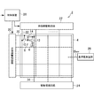
図1は実施形態に係る有機EL表示装置2の概略の構成を示す模式図である。有機EL表示装置2は、画像を表示する画素アレイ部4と、当該画素アレイ部を駆動する駆動部とを備える。有機EL表示装置2はガラス基板や可撓性を有した樹脂フィルムなどからなる基材の上に薄膜トランジスタ(thin film transistor:TFT)やOLEDなどの積層構造を形成されている。
画素アレイ部4には画素に対応してOLED6及び画素回路8がマトリクス状に配置される。画素回路8は複数のTFT10,12やキャパシタ14で構成される。
一方、駆動部は走査線駆動回路20、映像線駆動回路22、駆動電源回路24、基準電源回路26及び制御装置28を含み、画素回路8を駆動しOLED6の発光を制御するなどの機能を担う。
走査線駆動回路20は画素の水平方向の並び(画素行)ごとに設けられた走査信号線30に接続されている。走査線駆動回路20は制御装置28から入力されるタイミング信号に応じて走査信号線30を順番に選択し、選択した走査信号線30に、点灯TFT10をオンする電圧を印加する。
映像線駆動回路22は画素の垂直方向の並び(画素列)ごとに設けられた映像信号線32に接続されている。映像線駆動回路22は制御装置28から映像信号を入力され、走査線駆動回路20による走査信号線30の選択に合わせて、選択された画素行の映像信号に応じた電圧を各映像信号線32に出力する。当該電圧は、選択された画素行にて点灯TFT10を介してキャパシタ14に書き込まれる。駆動TFT12は書き込まれた電圧に応じた電流をOLED6に供給し、これにより、選択された走査信号線30に対応する画素のOLED6が発光する。
駆動電源回路24は画素列ごとに設けられた駆動電源線34に接続され、駆動電源線34及び選択された画素行の駆動TFT12を介してOLED6に電流を供給する。
基準電源回路26は、OLED6のカソード電極を構成する共通電極(図示せず)に定電位φREFを与える。φREFは例えば、接地電位GND(0V)に設定することができる。
本実施形態においてOLED6の下部電極は画素ごとに形成された画素電極であり、OLED6の上部電極が画素電極に対向配置された対向電極となる。下部電極は駆動TFT12に接続される。一方、上部電極は全画素のOLED6に共通の電極で構成される。本実施形態では下部電極がOLED6の陽極(アノード)であり、上部電極が陰極(カソード)である。
図2は有機EL表示装置2の表示パネル40の模式的な平面図である。表示パネル40の表示領域42に図1に示した画素アレイ部4が設けられ、上述したように画素アレイ部4にはOLEDが配列される。矩形である表示パネル40の一辺には部品実装領域46が設けられ、表示領域42につながる配線が配置される。さらに部品実装領域46には駆動部を構成するドライバIC48が搭載されたり、FPC50が接続されたりする。FPC50は制御装置28やその他の回路20,22,24,26等に接続されたり、その上にICを搭載されたりする。
本実施形態の表示パネル40はカラー画像を表示し、カラー画像における画素は例えば、赤色(R)、緑色(G)及び青色(B)に対応する光を出射する画素(サブピクセル)で構成される。
本実施形態ではR画素52r、G画素52g、B画素52bが表示領域にストライプ配列される例を説明する。当該配列では、画像の垂直方向に同じ種類(色)の画素が並び、水平方向にRGBが周期的に並ぶ。なお、図2においてR画素52r、G画素52g、B画素52bはそれぞれ有効な発光領域を模式的に示しており、構造上は画素開口60に対応し、それらの間の領域はバンクに対応している。
表示パネル40は例えば、TFT基板と対向基板とを、間に充填材を挟んで貼り合わせた構造とされる。TFT基板にはTFT72などからなる回路やOLED6などが形成される。対向基板には偏光板やタッチパネルが設けられ得る。また表示パネル40のカラー化方式がカラーフィルタ方式である場合、例えば、対向基板にはカラーフィルタが形成され、OLED6にて白色光を生成し、当該白色光をカラーフィルタを通すことでRGB各色を得る。
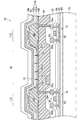
図3は図2に示すIII−III線に沿った位置での表示パネル40の模式的な垂直断面図である。図3は上述のTFT基板の断面構造を示しており、この上に形成される充填材層と対向基板の構造とは図示を省略されている。本実施形態において画素アレイ部4はトップエミッション型であり、TFT基板上に形成されたOLED6で生じた光を対向基板から出射する。すなわち、図3においてOLED6の光は上向きに出射する。
TFT基板の構造はガラスや樹脂フィルムからなる基材70の上に各種の層を積み重ね、またパターニングすることによって形成される。
具体的には基材70の上に窒化シリコン(SiNy)や酸化シリコン(SiOx)などの無機絶縁材料からなる下地層80を介してポリシリコン(p−Si)膜が形成され、当該p−Si膜をパターニングし、回路層で用いる箇所のp−Si膜を選択的に残す。例えば、p−Si膜を用いてトップゲート型のTFT72のチャネル部及びソース・ドレイン部となる半導体領域82が形成される。TFT72のチャネル部の上にはゲート絶縁膜84を介してゲート電極86が配置される。ゲート電極86はスパッタリング等で形成した金属膜をパターニングして形成される。この後、ゲート電極86を覆う層間絶縁膜88を積層する。TFT72のソース部、ドレイン部となるp−Siにはイオン注入により不純物が導入され、さらにそれらに電気的に接続されたソース電極90a及びドレイン電極90bが形成される。このようにしてTFT72を形成した後、層間絶縁膜92を積層する。層間絶縁膜92の表面には、スパッタリング等で形成した金属膜をパターニングして配線94等を形成することができ、当該金属膜とゲート電極86、ソース電極90a及びドレイン電極90bの形成に用いた金属膜とで例えば、図1に示した走査信号線30、映像信号線32、駆動電源線34を多層配線構造で形成することができる。この上に例えば、アクリル樹脂等の有機材料を積層して平坦化膜96が形成され、これにより平坦化された表示領域42の表面にOLED6が形成される。
OLED6は下部電極100、発光素子層102及び上部電極62で構成され、これら下部電極100、発光素子層102及び上部電極62は基材70側から順に積層される。
図3に示すTFT72がnチャネルを有した駆動TFT12であるとすると、下部電極100はTFT72のソース電極90aに接続される。具体的には、上述した平坦化膜96の形成後、下部電極100をTFT72に接続するためのコンタクトホール104が形成され、平坦化膜96表面及びコンタクトホール104内に形成した導電体膜をパターニングして、TFT72に接続された下部電極100が画素ごとに分離して形成される。
例えば、下部電極100はITO、IZOなどで形成される。また、本実施形態はトップエミッション型であるので、下部電極100は光反射率が高い材料で形成された反射層上に透明導電膜を積層した構造とすることができる。例えば、反射層はアルミニウム(Al)や銀(Ag)等で形成することができ、発光層からの光を表示面、つまり上部電極62側へ反射させる。
上述したように、駆動TFT12は各画素の映像信号に応じてOLED6に流れる電流を制御し、下部電極100は各画素の映像信号に応じた量のキャリアを発光素子層102へ供給する。具体的には本実施形態では下部電極100はアノードであり、キャリアとして正孔が下部電極100から発光素子層102へ供給される。
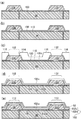
図4は、下部電極100の形成後の表示パネル40の製造工程の概略のプロセスフロー図であり、OLED6を形成する際の主要な工程におけるTFT基板の部分断面図を示している。以下、図4を用いてOLED6の形成工程を説明する。
下部電極100の形成後、バンク106を形成する(図4(a))。バンク106は例えば、アクリル、ポリイミド等の感光性樹脂をフォトリソグラフィ技術やインクジェット方式でパターニングして画素境界に形成され下部電極100間を電気的に分離する。なお、バンク106はSiNyやSiOxなどの無機絶縁材料で形成することもできる。バンク106で囲まれた領域が図2に示す画素開口60となり、当該領域には下部電極100が露出する。
バンク106の形成後、発光素子層102を構成する各層が下部電極100の上に順番に積層される。発光素子層102は注入されて発光する発光層(EML)、及び発光層への効率的にキャリアを供給する機能を担う補助層を含む。発光素子層102は補助層としてHIL及びHTLの少なくとも一方を含む。
例えば、OLED6はRGB画素それぞれの発光色に対応した単色発光のOLEDであり、アノードである下部電極100側から順にHIL、HTL、EML、ETLが積層された構造である。当該構造ではHIL、HTL及びETLが補助層である。このうちHIL及びHTLは正孔を供給するアノード(下部電極100)とEMLとの間に設けられる。図3では発光素子層102をHIL及びHTLからなる下層102dとEML及びETLからなる上層102uとに分けて示している。
バンク106の形成後、まず、下層102dが形成される。下層102dを構成するHTL/HILは例えば、ポリ(3,4−エチレンジオキシチオフェン)−ポリ(スチレンスルホン酸)(PEDOT−PSS)やその他の導電性有機材料で形成される。バンク106が形成された表示領域42の表面の全体に亘ってHTL/HIL層110が例えば、スパッタリングやCVDで成膜される(図4(b))。
しかる後、バンク106上にHTL/HIL層110の分断領域112が形成され(図4(c))、残る領域のHTL/HIL層110が発光素子層102の下層102dとなる(図4(d),(e))。分断領域112は隣接画素間でのHTL/HIL層110を介したキャリアの移動を阻害する機能を有する。図に示すように、分断領域112の幅はバンク106の幅の一部分で足り、下層102dの縁はバンク106の表面にオーバーラップさせることができる。
本実施形態では、分断領域112はHTL/HIL層110の非形成領域である。例えば、フォトリソグラフィ技術を用いたパターニングによりHTL/HIL層110を除去することで分断領域112が形成される。具体的には、HTL/HIL層110の表面にフォトレジスト膜を成膜し、当該フォトレジスト膜を用いて分断領域112を形成する領域に開口部114を備えたマスク116を形成する。そして、当該マスク116を用いて、開口部114からHTL/HIL層110をエッチング除去する(図4(c))。
なお、下層102dとして、印刷法などで当初から分断領域112を備えたパターンのHTL/HIL層110を形成することもできる。
次に下層102dの上にEML、ETLが表示領域42全体に亘って成膜され、上層102uが形成される(図4(d))。例えば、上層102uは蒸着により形成される。また、単色発光のOLEDではEMLは発光色ごとに異なる有機発光材料で形成される。この場合、EMLはインクジェット法などで形成することもできる。
下層102d及び上層102uからなる発光素子層102の上に上部電極62が例えば、スパッタリングで成膜される(図4(e))。上部電極62は基本的に表示領域42全体に亘って共通に形成される。
このようにしてOLED6が形成される。なお、上部電極62表面には図3に示すように封止膜108が形成される。封止膜108は、水分などの透過を阻止し、OLED6を保護する機能を有する。封止膜108として例えば、SiNy膜がCVD法によって成膜される。
なお、TFT基板に対向基板を貼り合わせない構造とすることもでき、この場合にはTFT基板の表面の機械的な強度を確保するため、封止膜108の上ないし下、または両方に保護膜を形成することができる。保護膜が下に形成される場合は、バンク106で生じる凹凸を平坦化させる効果を持たせ、封止膜108の凹凸を低減させてもよい。これにより封止膜の内部応力を低減させることができ、封止膜が剥がれにくい構造とすることができる。
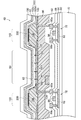
上述したように、有機EL表示装置2の駆動時には各画素のOLED6は映像信号に応じたキャリアを供給されて発光する。図5には当該駆動時にて下部電極100から発光素子層102へ供給されるキャリアである正孔の流れを矢印で模式的に示している。上部電極62は下部電極100より低い電位を印加され、各画素の下部電極100から発光素子層102の下層102dへ供給される正孔は基本的には当該下部電極100とこれに対向配置された上部電極62との間の電界に従い、矢印120で示すように発光素子層102の上層102uへ引き寄せられ当該画素のEMLに注入される。
一方、下部電極100から下層102dに供給された正孔の一部は矢印122で示すように画素開口60の外側へ向けて下層102d内を移動し得る。このキャリア移動が隣接する画素へのリーク電流となると上述した問題を生じる。この点、有機EL表示装置2では発光素子層102の下層102dは画素境界に分断領域112を形成されていることにより、隣接画素へのリーク電流の到達を阻止することができ、リーク電流による隣接画素の発光が防止される。よって、画像の解像度の低下が抑制される。また、分断領域112を発光色が異なる画素間の境界に配置することで、リーク電流による混色が抑制され高い色純度が得られ、好適な色再現性を実現できる。
なお、補助層のうち下層102dを構成するものは他の補助層より比較的厚く形成されることが多く、それに伴い下層102d内を移動してリーク電流となるキャリア量が大きくなる。この点、本実施形態では下層102dに分断領域112を設けることで、画素間のリーク電流を好適に抑制することができる。
また、OLED6は白色発光とすることもできる。例えば、白色発光のOLED6は発光色が異なる複数のOLEDを光透過性の中間層を介して電気的に直列接続したタンデム構造とすることができる。タンデム構造では中間層として設けられる電荷発生層(charge generation layer:CGL)もHIL、HTL等と同様、キャリア移動性を有する補助層である。本発明はタンデム構造のOLED6を有する有機EL表示装置2に適用することもできる。この場合も上述の単色発光のOLED6と同様、下部電極100の上に積層されるHTL/HIL層110に分断領域112が設けられ、これにより画素間のリーク電流を好適に抑制することができる。
分断領域112は各画素を取り囲む画素境界の全周に沿って配置することができる。すなわち、HTL/HIL層110が分断領域112により画素ごとに分かれた構造とすることができる。
また、既に述べたように分断領域112を発光色が互いに異なる隣接画素間の境界に沿って配置することにより好適な色再現性を実現できる。例えば、本実施形態ではRGB画素がストライプ配列され、行方向に隣り合う各画素対は互いに発光色が異なる。この場合、分断領域112を列方向に延びる画素境界に沿って設けることで隣接画素間の混色を防止できる。
なお、分断領域112は発光色が互いに異なる隣接画素間の境界の全体に沿ってではなく一部のみに沿って形成されてもよい。
さて、表示パネル40の製造では、生産効率を高めるために、1枚の大きな基材70上に複数面の表示パネル40を同時に形成する手法が採用される。この製造手法では基材上へのTFTの形成などの工程は複数面の表示パネル40を一体に行われ、一方、OLED形成工程は複数面の表示パネル40を分割して行われる。つまり、この製造方法は、複数面の表示パネル40がつながった状態で加工される前段工程と、表示パネル40ごとに分割されて残りの加工が施される後段工程とに分けられ、ここでは前段工程をTFT工程、後段工程をOLED工程と呼ぶ。
TFT工程は基本的に、集積回路などを製造する半導体製造プロセスを利用して行うことができる工程からなり、比較的にプロセス条件の自由度が高く、例えば、数百℃程度の高温プロセスを利用するように製造工程を設計することも可能である。一方、OLED工程は、有機材料からなる発光素子層の劣化を防ぐため、雰囲気温度の上限が数十℃程度に制限され得る。つまり、OLED工程は、表示パネル40をそれぞれ加工することにより工数が増加し、またTFT工程に比べてより確実にプロセス条件を制御する必要がある。そのため、表示パネル40の製造工程においてTFT工程の占める割合を大きくし、OLED工程の占める割合を小さくすることで、表示パネル40の製造コストの低減や製造期間の短縮を図ることができる。
本実施形態では、図4(a)に示す構造を形成する工程がTFT工程として行われる。すなわち、基材70の上にTFT72などからなる回路を形成し、その上に平坦化膜96を積層し、また下部電極100及びバンク106が形成される。
本実施形態では、さらに発光素子層102の下層102dを形成する工程がTFT工程として行われ、これにより、上に述べた製造コスト低減や製造期間短縮の効果が得られる。つまり、境界領域にバンク106が形成された後、さらにTFT工程において、表示領域42の全面にHTL/HIL層110を形成し(図4(b))、HTL/HIL層110の上にマスク116を形成し、このマスク116を用いて分断領域112を形成する。
なお、OLED工程は発光素子層102の上層102uを形成する工程(図4(d))、上部電極62を形成する工程(図4(e))、及びその後の工程を含む。
[第2の実施形態]
以下、本発明の第2の実施形態に係る有機EL表示装置2bを説明する。本実施形態と上記第1の実施形態とは分断領域112の構造及び形成方法に相違点を有し、その他の点では基本的に共通である。以下、第2の実施形態について第1の実施形態との相違点を中心に説明する。
有機EL表示装置2bの表示パネル40の模式的な平面図は、第1の実施形態について示した図2と基本的には同じであり、これを援用する。図5は図2に示すIII−III線に沿った位置での本実施形態の表示パネル40の模式的な垂直断面図である。第1の実施形態の分断領域112は、発光素子層102におけるHTL/HIL層110といったキャリア移動性を有した補助層である下層102dが存在しない領域であった。これに対し、本実施形態の分断領域112は、下層102dにおいてその材料の変質・変性によりキャリア移動性を喪失した領域であり、図5においてバンク106の上の分断領域112には、キャリア移動性を喪失した下層102dである変質層200が存在する。
例えば、第1の実施形態と同様にして下層102d、及び分断領域112を形成する領域に開口部114を備えたマスク116を形成する(図4(c))。本実施形態では当該マスク116を用いて、例えば、イオン注入やエネルギー線照射を行う。これにより、開口部114の下層102d(HTL/HIL層110)に化学的変化を起こさせたり、分子構造の破壊を起こさせたりすることで、下層102dが有していた導電性を失わせ変質層200を形成する。
変質層200を形成した後は、第1の実施形態における有機EL表示装置2と基本的に同様の工程で本実施形態の有機EL表示装置2bが完成される。例えば、変質層200の形成後、まず上層102uを積層して発光素子層102を形成し(図4(d))、次に発光素子層102の上に上部電極62を形成してOLED6が形成される(図4(e))。
上記各実施形態ではRGB画素がストライプ配列された有機EL表示装置2にて分断領域112を設けてリーク電流を抑制する構造を説明したが、当該リーク電流抑制構造は他の画素配列においても適用することができる。
また上記各実施形態及び変形例では、下部電極100がOLED6のアノード、上部電極62がOLED6のカソードである場合を説明した。しかし、本発明は、下部電極100がOLED6のカソード、上部電極62がOLED6のアノードである場合にも適用できる。その場合、発光素子層102における各層の積層順序は上述の構成とは逆転する。例えば、カソードである下部電極100側から順にEIL、ETL、EML、HTL、HILが積層された構造となる。
本発明の実施形態として上述した有機EL表示装置2,2bを基にして、当業者が適宜設計変更して実施し得る全ての有機EL表示装置も、本発明の要旨を包含する限り、本発明の範囲に属する。また、有機EL表示装置以外の表示装置、例えば発光層として量子ドット素子を採用した量子ドット表示装置等も本発明の範囲に属する。
本発明の思想の範疇において、当業者であれば、各種の変更例及び修正例に想到し得るものであり、それら変更例及び修正例についても本発明の範囲に属するものと了解される。例えば、前述の各実施形態に対して、当業者が適宜、構成要素の追加、削除若しくは設計変更を行ったもの、又は、工程の追加、省略若しくは条件変更を行ったものも、本発明の要旨を備えている限り、本発明の範囲に含まれる。
また、本実施形態において述べた態様によりもたらされる他の作用効果について本明細書記載から明らかなもの、又は当業者において適宜想到し得るものついては、当然に本発明によりもたらされるものと解される。