JP2016103395A - Display device - Google Patents
Display device Download PDFInfo
- Publication number
- JP2016103395A JP2016103395A JP2014240887A JP2014240887A JP2016103395A JP 2016103395 A JP2016103395 A JP 2016103395A JP 2014240887 A JP2014240887 A JP 2014240887A JP 2014240887 A JP2014240887 A JP 2014240887A JP 2016103395 A JP2016103395 A JP 2016103395A
- Authority
- JP
- Japan
- Prior art keywords
- layer
- display device
- light emitting
- pixel
- emitting element
- Prior art date
- Legal status (The legal status is an assumption and is not a legal conclusion. Google has not performed a legal analysis and makes no representation as to the accuracy of the status listed.)
- Pending
Links
- 239000000463 material Substances 0.000 claims abstract description 12
- 238000002347 injection Methods 0.000 claims abstract description 6
- 239000007924 injection Substances 0.000 claims abstract description 6
- 239000000758 substrate Substances 0.000 claims description 21
- 239000000969 carrier Substances 0.000 claims description 10
- 239000003086 colorant Substances 0.000 claims description 8
- 238000000059 patterning Methods 0.000 claims description 5
- 230000008859 change Effects 0.000 claims description 2
- 239000000243 solution Substances 0.000 abstract 1
- 239000010410 layer Substances 0.000 description 122
- 238000000034 method Methods 0.000 description 43
- 239000010408 film Substances 0.000 description 36
- 230000008569 process Effects 0.000 description 34
- 238000005401 electroluminescence Methods 0.000 description 23
- 238000004519 manufacturing process Methods 0.000 description 14
- 230000015572 biosynthetic process Effects 0.000 description 8
- 238000007789 sealing Methods 0.000 description 8
- 238000004544 sputter deposition Methods 0.000 description 5
- 238000005229 chemical vapour deposition Methods 0.000 description 4
- 239000011229 interlayer Substances 0.000 description 4
- 229910052751 metal Inorganic materials 0.000 description 4
- 239000002184 metal Substances 0.000 description 4
- 238000012986 modification Methods 0.000 description 4
- 230000004048 modification Effects 0.000 description 4
- 239000003990 capacitor Substances 0.000 description 3
- 238000010586 diagram Methods 0.000 description 3
- 239000011368 organic material Substances 0.000 description 3
- 230000002829 reductive effect Effects 0.000 description 3
- 239000011347 resin Substances 0.000 description 3
- 229920005989 resin Polymers 0.000 description 3
- 239000004065 semiconductor Substances 0.000 description 3
- 238000013461 design Methods 0.000 description 2
- 230000000694 effects Effects 0.000 description 2
- 239000000945 filler Substances 0.000 description 2
- 239000011521 glass Substances 0.000 description 2
- 239000011810 insulating material Substances 0.000 description 2
- 238000005468 ion implantation Methods 0.000 description 2
- 239000011159 matrix material Substances 0.000 description 2
- 238000000206 photolithography Methods 0.000 description 2
- 229920002120 photoresistant polymer Polymers 0.000 description 2
- 230000001681 protective effect Effects 0.000 description 2
- 239000002096 quantum dot Substances 0.000 description 2
- LIVNPJMFVYWSIS-UHFFFAOYSA-N silicon monoxide Chemical compound [Si-]#[O+] LIVNPJMFVYWSIS-UHFFFAOYSA-N 0.000 description 2
- 238000007740 vapor deposition Methods 0.000 description 2
- 239000004925 Acrylic resin Substances 0.000 description 1
- 229920000178 Acrylic resin Polymers 0.000 description 1
- 229920001609 Poly(3,4-ethylenedioxythiophene) Polymers 0.000 description 1
- 239000004642 Polyimide Substances 0.000 description 1
- 229910052581 Si3N4 Inorganic materials 0.000 description 1
- VYPSYNLAJGMNEJ-UHFFFAOYSA-N Silicium dioxide Chemical compound O=[Si]=O VYPSYNLAJGMNEJ-UHFFFAOYSA-N 0.000 description 1
- BQCADISMDOOEFD-UHFFFAOYSA-N Silver Chemical compound [Ag] BQCADISMDOOEFD-UHFFFAOYSA-N 0.000 description 1
- NIXOWILDQLNWCW-UHFFFAOYSA-N acrylic acid group Chemical group C(C=C)(=O)O NIXOWILDQLNWCW-UHFFFAOYSA-N 0.000 description 1
- 230000004075 alteration Effects 0.000 description 1
- 229910052782 aluminium Inorganic materials 0.000 description 1
- XAGFODPZIPBFFR-UHFFFAOYSA-N aluminium Chemical compound [Al] XAGFODPZIPBFFR-UHFFFAOYSA-N 0.000 description 1
- 238000013459 approach Methods 0.000 description 1
- 230000005540 biological transmission Effects 0.000 description 1
- 230000000903 blocking effect Effects 0.000 description 1
- 239000004020 conductor Substances 0.000 description 1
- 230000003247 decreasing effect Effects 0.000 description 1
- 238000004925 denaturation Methods 0.000 description 1
- 230000036425 denaturation Effects 0.000 description 1
- 230000006866 deterioration Effects 0.000 description 1
- 230000005684 electric field Effects 0.000 description 1
- 230000005525 hole transport Effects 0.000 description 1
- 239000012535 impurity Substances 0.000 description 1
- 230000002401 inhibitory effect Effects 0.000 description 1
- 239000000203 mixture Substances 0.000 description 1
- 150000002894 organic compounds Chemical class 0.000 description 1
- 230000036961 partial effect Effects 0.000 description 1
- 229920000172 poly(styrenesulfonic acid) Polymers 0.000 description 1
- 229910021420 polycrystalline silicon Inorganic materials 0.000 description 1
- 229920001721 polyimide Polymers 0.000 description 1
- 229920005591 polysilicon Polymers 0.000 description 1
- 238000012545 processing Methods 0.000 description 1
- 238000000926 separation method Methods 0.000 description 1
- HQVNEWCFYHHQES-UHFFFAOYSA-N silicon nitride Chemical compound N12[Si]34N5[Si]62N3[Si]51N64 HQVNEWCFYHHQES-UHFFFAOYSA-N 0.000 description 1
- 229910052814 silicon oxide Inorganic materials 0.000 description 1
- 229910052709 silver Inorganic materials 0.000 description 1
- 239000004332 silver Substances 0.000 description 1
- 239000000126 substance Substances 0.000 description 1
- 230000001629 suppression Effects 0.000 description 1
- 239000010409 thin film Substances 0.000 description 1
Images

Classifications
-
- H—ELECTRICITY
- H10—SEMICONDUCTOR DEVICES; ELECTRIC SOLID-STATE DEVICES NOT OTHERWISE PROVIDED FOR
- H10K—ORGANIC ELECTRIC SOLID-STATE DEVICES
- H10K59/00—Integrated devices, or assemblies of multiple devices, comprising at least one organic light-emitting element covered by group H10K50/00
- H10K59/10—OLED displays
- H10K59/12—Active-matrix OLED [AMOLED] displays
- H10K59/121—Active-matrix OLED [AMOLED] displays characterised by the geometry or disposition of pixel elements
- H10K59/1213—Active-matrix OLED [AMOLED] displays characterised by the geometry or disposition of pixel elements the pixel elements being TFTs
-
- H—ELECTRICITY
- H10—SEMICONDUCTOR DEVICES; ELECTRIC SOLID-STATE DEVICES NOT OTHERWISE PROVIDED FOR
- H10K—ORGANIC ELECTRIC SOLID-STATE DEVICES
- H10K59/00—Integrated devices, or assemblies of multiple devices, comprising at least one organic light-emitting element covered by group H10K50/00
- H10K59/30—Devices specially adapted for multicolour light emission
- H10K59/35—Devices specially adapted for multicolour light emission comprising red-green-blue [RGB] subpixels
-
- H—ELECTRICITY
- H10—SEMICONDUCTOR DEVICES; ELECTRIC SOLID-STATE DEVICES NOT OTHERWISE PROVIDED FOR
- H10K—ORGANIC ELECTRIC SOLID-STATE DEVICES
- H10K50/00—Organic light-emitting devices
- H10K50/10—OLEDs or polymer light-emitting diodes [PLED]
- H10K50/14—Carrier transporting layers
- H10K50/15—Hole transporting layers
-
- H—ELECTRICITY
- H10—SEMICONDUCTOR DEVICES; ELECTRIC SOLID-STATE DEVICES NOT OTHERWISE PROVIDED FOR
- H10K—ORGANIC ELECTRIC SOLID-STATE DEVICES
- H10K50/00—Organic light-emitting devices
- H10K50/10—OLEDs or polymer light-emitting diodes [PLED]
- H10K50/17—Carrier injection layers
-
- H—ELECTRICITY
- H10—SEMICONDUCTOR DEVICES; ELECTRIC SOLID-STATE DEVICES NOT OTHERWISE PROVIDED FOR
- H10K—ORGANIC ELECTRIC SOLID-STATE DEVICES
- H10K59/00—Integrated devices, or assemblies of multiple devices, comprising at least one organic light-emitting element covered by group H10K50/00
- H10K59/10—OLED displays
- H10K59/12—Active-matrix OLED [AMOLED] displays
- H10K59/122—Pixel-defining structures or layers, e.g. banks
Landscapes
- Physics & Mathematics (AREA)
- Engineering & Computer Science (AREA)
- Microelectronics & Electronic Packaging (AREA)
- Optics & Photonics (AREA)
- Geometry (AREA)
- Electroluminescent Light Sources (AREA)
- Devices For Indicating Variable Information By Combining Individual Elements (AREA)
Abstract
Description
本発明は電圧印加により発光する自発光素子を用いた表示装置に関する。 The present invention relates to a display device using a self-luminous element that emits light when voltage is applied.
表示装置として、有機エレクトロルミネッセンス(electroluminescence:EL)素子などの自発光素子を用いたものの開発が進められている。有機エレクトロルミネッセンス素子は一般にOLED(organic light emitting diode)と称され、発光ダイオードの一種である。OLEDは有機化合物からなる発光層にキャリア(電子や正孔)を注入され発光する。OLEDは電圧の印加時に発光層に効率的にキャリアが注入されるように、電極と発光層との間などに、キャリア移動性を有した補助的な層を設ける構造とされることが一般的となっている。 As a display device, a device using a self-luminous element such as an organic electroluminescence (EL) element has been developed. The organic electroluminescence element is generally called an OLED (organic light emitting diode) and is a kind of light emitting diode. OLED emits light by injecting carriers (electrons and holes) into a light emitting layer made of an organic compound. In general, an OLED has a structure in which an auxiliary layer having carrier mobility is provided between an electrode and a light emitting layer so that carriers are efficiently injected into the light emitting layer when a voltage is applied. It has become.
例えば、補助的な層として、アノードと発光層(emitting layer:EML)との間に、正孔輸送層(hole transport layer:HTL)や正孔注入層(hole injection layer:HIL)が設けられる。また、カソードと発光層との間には、電子輸送層(electron transport layer:ETL)や電子注入層(electron injection layer:EIL)が設けられる。これら補助層はCVD(chemical vapor deposition)法、スパッタ法、蒸着法などにより、複数の画素が配列された画像表示領域全体に亘って共通に形成される。 For example, as an auxiliary layer, a hole transport layer (HTL) or a hole injection layer (HIL) is provided between an anode and an emitting layer (EML). An electron transport layer (electron transport layer: ETL) or an electron injection layer (electron injection layer: EIL) is provided between the cathode and the light emitting layer. These auxiliary layers are formed in common over the entire image display area in which a plurality of pixels are arranged by CVD (chemical vapor deposition), sputtering, vapor deposition, or the like.
上述したOLEDにおけるHTL,HILのようなキャリア移動性を有した層が画像表示領域に亘って連続する共通層として形成される発光素子を用いた表示装置は、当該共通層を通して隣接する画素間でのキャリアのリークが発生し得る。隣接画素へのリーク電流は当該隣接画素の意図しない発光を招くという問題があった。具体的には、リーク電流は画像の解像度の劣化を生じるほか、発光色が異なる画素間におけるリーク電流は色再現性(色純度)の低下を生じるという問題があった。特に、画素サイズの縮小による高精細化に伴い隣接画素の開口部(又は発光領域)が接近することにより当該問題が顕著となる。 A display device using a light-emitting element in which a layer having carrier mobility such as HTL and HIL in the OLED described above is formed as a common layer continuous over the image display region is used between adjacent pixels through the common layer. Carrier leakage may occur. There is a problem that leakage current to an adjacent pixel causes unintended light emission of the adjacent pixel. Specifically, the leak current causes a problem that the resolution of the image is deteriorated, and the leak current between pixels having different emission colors causes a decrease in color reproducibility (color purity). In particular, the problem becomes conspicuous when the opening (or light emitting region) of an adjacent pixel approaches as the pixel size is reduced and the definition is increased.
本発明は上記問題点を解決するためになされたものであり、隣接する画素の自発光素子へのリーク電流が抑制され、隣接画素の意図しない発光が防止される表示装置を提供することを目的とする。 The present invention has been made to solve the above-described problems, and an object of the present invention is to provide a display device in which leakage current to the self-luminous elements of adjacent pixels is suppressed and unintentional light emission of adjacent pixels is prevented. And
本発明に係る表示装置は、基材上に画像表示領域を備え、前記画像表示領域に画素となる発光領域が複数配列された表示装置であって、前記各画素に映像信号に応じた量のキャリアを供給する画素電極と、前記画素の境界に沿って形成されたバンクと、キャリア輸送層又はキャリア注入層を含むキャリア移動性を有した層であり前記画素電極及び前記バンク上に積層された補助層と当該補助層の上に積層され前記キャリアを注入されて発光する発光層とを含む発光素子層と、前記発光素子層の上に配置され前記画素電極と共に前記発光素子層に電圧を印加する対向電極と、を有し、前記補助層には前記バンク上に分断領域が設けられ、当該分断領域は隣接画素間での前記補助層を介した前記キャリアの移動を阻害する。 A display device according to the present invention is a display device including an image display region on a base material, and a plurality of light emitting regions serving as pixels arranged in the image display region, wherein each pixel has an amount corresponding to a video signal. A pixel electrode that supplies carriers, a bank formed along the boundary of the pixel, and a carrier mobility layer including a carrier transport layer or a carrier injection layer, and is stacked on the pixel electrode and the bank. A light emitting element layer including an auxiliary layer and a light emitting layer that is laminated on the auxiliary layer and emits light by injecting the carrier, and a voltage is applied to the light emitting element layer together with the pixel electrode disposed on the light emitting element layer The auxiliary layer is provided with a dividing region on the bank, and the dividing region inhibits the movement of the carriers through the auxiliary layer between adjacent pixels.
以下、本発明の実施の形態(以下実施形態という)について、図面に基づいて説明する。 Hereinafter, embodiments of the present invention (hereinafter referred to as embodiments) will be described with reference to the drawings.
なお、開示はあくまで一例にすぎず、当業者において、発明の主旨を保っての適宜変更について容易に想到し得るものについては、当然に本発明の範囲に含有されるものである。また、図面は説明をより明確にするため、実際の態様に比べ、各部の幅、厚さ、形状等について模式的に表される場合があるが、あくまで一例であって、本発明の解釈を限定するものではない。また、本明細書と各図において、既出の図に関して前述したものと同様の要素には、同一の符号を付して、詳細な説明を適宜省略することがある。 It should be noted that the disclosure is merely an example, and those skilled in the art can easily conceive of appropriate modifications while maintaining the gist of the invention are naturally included in the scope of the present invention. In addition, the drawings may be schematically represented with respect to the width, thickness, shape, and the like of each part in comparison with actual aspects for the sake of clarity of explanation, but are merely examples, and the interpretation of the present invention is not limited. It is not limited. In addition, in the present specification and each drawing, elements similar to those described above with reference to the previous drawings are denoted by the same reference numerals, and detailed description may be omitted as appropriate.
以下に説明する各実施形態の表示装置は有機EL表示装置である。有機EL表示装置は、アクティブマトリックス型表示装置であり、テレビ、パソコン、携帯端末、携帯電話等に搭載される。 The display device of each embodiment described below is an organic EL display device. The organic EL display device is an active matrix display device and is mounted on a television, a personal computer, a mobile terminal, a mobile phone, or the like.
表示装置の画像表示領域には、画像を構成する複数の画素が2次元配列される。ここで、画像に対応する2次元の直交座標系の1つの座標軸に沿った方向を行方向、もう1つの座標軸に沿った方向を列方向とする。以降の説明では、行方向、列方向は基本的には画像の水平方向、垂直方向とするが、これは便宜的な定義である。例えば、同一の画像表示領域にて画像の縦横を切り換えて表示することができる表示装置では、画像表示領域の行方向、列方向はそれぞれ画像の垂直方向、水平方向となる場合がある。また、表示装置の構造自体も、以下に説明するものに対し行方向と列方向とを入れ替えたものとすることができる。 A plurality of pixels constituting an image are two-dimensionally arranged in the image display area of the display device. Here, a direction along one coordinate axis of the two-dimensional orthogonal coordinate system corresponding to the image is a row direction, and a direction along the other coordinate axis is a column direction. In the following description, the row direction and the column direction are basically the horizontal and vertical directions of the image, but this is a convenient definition. For example, in a display device that can switch between vertical and horizontal images in the same image display area, the row direction and column direction of the image display area may be the vertical direction and horizontal direction of the image, respectively. Also, the structure of the display device itself can be the one described in the following, with the row direction and the column direction being interchanged.
また、以下の実施形態では、画像表示領域には発光色が互いに異なる複数種類の画素(サブピクセル)が配列されカラー画像を表示可能な表示装置を説明する。なお、カラー画像における画素は、表示装置における複数種類のサブピクセルからなる一組のサブピクセルに対応するが、表示装置ではサブピクセルが構成上の単位であり、例えば、サブピクセルごとにOLEDや画素回路が形成される。そこで以下の説明では、基本的にサブピクセルを画素と扱う。 In the following embodiments, a display device capable of displaying a color image by arranging a plurality of types of pixels (sub-pixels) having different emission colors in the image display area will be described. Note that the pixels in the color image correspond to a set of subpixels composed of a plurality of types of subpixels in the display device. However, in the display device, the subpixels are structural units. For example, an OLED or a pixel is provided for each subpixel. A circuit is formed. Therefore, in the following description, subpixels are basically treated as pixels.
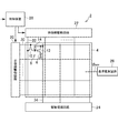
[第1の実施形態]
図1は実施形態に係る有機EL表示装置2の概略の構成を示す模式図である。有機EL表示装置2は、画像を表示する画素アレイ部4と、当該画素アレイ部を駆動する駆動部とを備える。有機EL表示装置2はガラス基板や可撓性を有した樹脂フィルムなどからなる基材の上に薄膜トランジスタ(thin film transistor:TFT)やOLEDなどの積層構造を形成されている。
[First Embodiment]
FIG. 1 is a schematic diagram illustrating a schematic configuration of an organic EL display device 2 according to the embodiment. The organic EL display device 2 includes a pixel array unit 4 that displays an image and a drive unit that drives the pixel array unit. In the organic EL display device 2, a laminated structure such as a thin film transistor (TFT) or an OLED is formed on a substrate made of a glass substrate or a flexible resin film.
画素アレイ部4には画素に対応してOLED6及び画素回路8がマトリクス状に配置される。画素回路8は複数のTFT10,12やキャパシタ14で構成される。
In the pixel array unit 4,
一方、駆動部は走査線駆動回路20、映像線駆動回路22、駆動電源回路24、基準電源回路26及び制御装置28を含み、画素回路8を駆動しOLED6の発光を制御するなどの機能を担う。
On the other hand, the drive unit includes a scanning
走査線駆動回路20は画素の水平方向の並び(画素行)ごとに設けられた走査信号線30に接続されている。走査線駆動回路20は制御装置28から入力されるタイミング信号に応じて走査信号線30を順番に選択し、選択した走査信号線30に、点灯TFT10をオンする電圧を印加する。
The scanning
映像線駆動回路22は画素の垂直方向の並び(画素列)ごとに設けられた映像信号線32に接続されている。映像線駆動回路22は制御装置28から映像信号を入力され、走査線駆動回路20による走査信号線30の選択に合わせて、選択された画素行の映像信号に応じた電圧を各映像信号線32に出力する。当該電圧は、選択された画素行にて点灯TFT10を介してキャパシタ14に書き込まれる。駆動TFT12は書き込まれた電圧に応じた電流をOLED6に供給し、これにより、選択された走査信号線30に対応する画素のOLED6が発光する。
The video line driving circuit 22 is connected to a
駆動電源回路24は画素列ごとに設けられた駆動電源線34に接続され、駆動電源線34及び選択された画素行の駆動TFT12を介してOLED6に電流を供給する。
The drive
基準電源回路26は、OLED6のカソード電極を構成する共通電極(図示せず)に定電位φREFを与える。φREFは例えば、接地電位GND(0V)に設定することができる。
The reference
本実施形態においてOLED6の下部電極は画素ごとに形成された画素電極であり、OLED6の上部電極が画素電極に対向配置された対向電極となる。下部電極は駆動TFT12に接続される。一方、上部電極は全画素のOLED6に共通の電極で構成される。本実施形態では下部電極がOLED6の陽極(アノード)であり、上部電極が陰極(カソード)である。
In the present embodiment, the lower electrode of the
図2は有機EL表示装置2の表示パネル40の模式的な平面図である。表示パネル40の表示領域42に図1に示した画素アレイ部4が設けられ、上述したように画素アレイ部4にはOLEDが配列される。矩形である表示パネル40の一辺には部品実装領域46が設けられ、表示領域42につながる配線が配置される。さらに部品実装領域46には駆動部を構成するドライバIC48が搭載されたり、FPC50が接続されたりする。FPC50は制御装置28やその他の回路20,22,24,26等に接続されたり、その上にICを搭載されたりする。
FIG. 2 is a schematic plan view of the
本実施形態の表示パネル40はカラー画像を表示し、カラー画像における画素は例えば、赤色(R)、緑色(G)及び青色(B)に対応する光を出射する画素(サブピクセル)で構成される。
The
本実施形態ではR画素52r、G画素52g、B画素52bが表示領域にストライプ配列される例を説明する。当該配列では、画像の垂直方向に同じ種類(色)の画素が並び、水平方向にRGBが周期的に並ぶ。なお、図2においてR画素52r、G画素52g、B画素52bはそれぞれ有効な発光領域を模式的に示しており、構造上は画素開口60に対応し、それらの間の領域はバンクに対応している。
In the present embodiment, an example will be described in which the
表示パネル40は例えば、TFT基板と対向基板とを、間に充填材を挟んで貼り合わせた構造とされる。TFT基板にはTFT72などからなる回路やOLED6などが形成される。対向基板には偏光板やタッチパネルが設けられ得る。また表示パネル40のカラー化方式がカラーフィルタ方式である場合、例えば、対向基板にはカラーフィルタが形成され、OLED6にて白色光を生成し、当該白色光をカラーフィルタを通すことでRGB各色を得る。
The
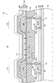
図3は図2に示すIII−III線に沿った位置での表示パネル40の模式的な垂直断面図である。図3は上述のTFT基板の断面構造を示しており、この上に形成される充填材層と対向基板の構造とは図示を省略されている。本実施形態において画素アレイ部4はトップエミッション型であり、TFT基板上に形成されたOLED6で生じた光を対向基板から出射する。すなわち、図3においてOLED6の光は上向きに出射する。
FIG. 3 is a schematic vertical sectional view of the
TFT基板の構造はガラスや樹脂フィルムからなる基材70の上に各種の層を積み重ね、またパターニングすることによって形成される。
The structure of the TFT substrate is formed by stacking and patterning various layers on a
具体的には基材70の上に窒化シリコン(SiNy)や酸化シリコン(SiOx)などの無機絶縁材料からなる下地層80を介してポリシリコン(p−Si)膜が形成され、当該p−Si膜をパターニングし、回路層で用いる箇所のp−Si膜を選択的に残す。例えば、p−Si膜を用いてトップゲート型のTFT72のチャネル部及びソース・ドレイン部となる半導体領域82が形成される。TFT72のチャネル部の上にはゲート絶縁膜84を介してゲート電極86が配置される。ゲート電極86はスパッタリング等で形成した金属膜をパターニングして形成される。この後、ゲート電極86を覆う層間絶縁膜88を積層する。TFT72のソース部、ドレイン部となるp−Siにはイオン注入により不純物が導入され、さらにそれらに電気的に接続されたソース電極90a及びドレイン電極90bが形成される。このようにしてTFT72を形成した後、層間絶縁膜92を積層する。層間絶縁膜92の表面には、スパッタリング等で形成した金属膜をパターニングして配線94等を形成することができ、当該金属膜とゲート電極86、ソース電極90a及びドレイン電極90bの形成に用いた金属膜とで例えば、図1に示した走査信号線30、映像信号線32、駆動電源線34を多層配線構造で形成することができる。この上に例えば、アクリル樹脂等の有機材料を積層して平坦化膜96が形成され、これにより平坦化された表示領域42の表面にOLED6が形成される。
Specifically, a polysilicon (p-Si) film is formed on the
OLED6は下部電極100、発光素子層102及び上部電極62で構成され、これら下部電極100、発光素子層102及び上部電極62は基材70側から順に積層される。
The
図3に示すTFT72がnチャネルを有した駆動TFT12であるとすると、下部電極100はTFT72のソース電極90aに接続される。具体的には、上述した平坦化膜96の形成後、下部電極100をTFT72に接続するためのコンタクトホール104が形成され、平坦化膜96表面及びコンタクトホール104内に形成した導電体膜をパターニングして、TFT72に接続された下部電極100が画素ごとに分離して形成される。
If the
例えば、下部電極100はITO、IZOなどで形成される。また、本実施形態はトップエミッション型であるので、下部電極100は光反射率が高い材料で形成された反射層上に透明導電膜を積層した構造とすることができる。例えば、反射層はアルミニウム(Al)や銀(Ag)等で形成することができ、発光層からの光を表示面、つまり上部電極62側へ反射させる。
For example, the
上述したように、駆動TFT12は各画素の映像信号に応じてOLED6に流れる電流を制御し、下部電極100は各画素の映像信号に応じた量のキャリアを発光素子層102へ供給する。具体的には本実施形態では下部電極100はアノードであり、キャリアとして正孔が下部電極100から発光素子層102へ供給される。
As described above, the driving
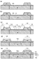
図4は、下部電極100の形成後の表示パネル40の製造工程の概略のプロセスフロー図であり、OLED6を形成する際の主要な工程におけるTFT基板の部分断面図を示している。以下、図4を用いてOLED6の形成工程を説明する。
FIG. 4 is a schematic process flow diagram of the manufacturing process of the
下部電極100の形成後、バンク106を形成する(図4(a))。バンク106は例えば、アクリル、ポリイミド等の感光性樹脂をフォトリソグラフィ技術やインクジェット方式でパターニングして画素境界に形成され下部電極100間を電気的に分離する。なお、バンク106はSiNyやSiOxなどの無機絶縁材料で形成することもできる。バンク106で囲まれた領域が図2に示す画素開口60となり、当該領域には下部電極100が露出する。
After the formation of the
バンク106の形成後、発光素子層102を構成する各層が下部電極100の上に順番に積層される。発光素子層102は注入されて発光する発光層(EML)、及び発光層への効率的にキャリアを供給する機能を担う補助層を含む。発光素子層102は補助層としてHIL及びHTLの少なくとも一方を含む。
After the formation of the
例えば、OLED6はRGB画素それぞれの発光色に対応した単色発光のOLEDであり、アノードである下部電極100側から順にHIL、HTL、EML、ETLが積層された構造である。当該構造ではHIL、HTL及びETLが補助層である。このうちHIL及びHTLは正孔を供給するアノード(下部電極100)とEMLとの間に設けられる。図3では発光素子層102をHIL及びHTLからなる下層102dとEML及びETLからなる上層102uとに分けて示している。
For example, the
バンク106の形成後、まず、下層102dが形成される。下層102dを構成するHTL/HILは例えば、ポリ(3,4−エチレンジオキシチオフェン)−ポリ(スチレンスルホン酸)(PEDOT−PSS)やその他の導電性有機材料で形成される。バンク106が形成された表示領域42の表面の全体に亘ってHTL/HIL層110が例えば、スパッタリングやCVDで成膜される(図4(b))。
After the formation of the
しかる後、バンク106上にHTL/HIL層110の分断領域112が形成され(図4(c))、残る領域のHTL/HIL層110が発光素子層102の下層102dとなる(図4(d),(e))。分断領域112は隣接画素間でのHTL/HIL層110を介したキャリアの移動を阻害する機能を有する。図に示すように、分断領域112の幅はバンク106の幅の一部分で足り、下層102dの縁はバンク106の表面にオーバーラップさせることができる。
Thereafter, the divided
本実施形態では、分断領域112はHTL/HIL層110の非形成領域である。例えば、フォトリソグラフィ技術を用いたパターニングによりHTL/HIL層110を除去することで分断領域112が形成される。具体的には、HTL/HIL層110の表面にフォトレジスト膜を成膜し、当該フォトレジスト膜を用いて分断領域112を形成する領域に開口部114を備えたマスク116を形成する。そして、当該マスク116を用いて、開口部114からHTL/HIL層110をエッチング除去する(図4(c))。
In the present embodiment, the dividing
なお、下層102dとして、印刷法などで当初から分断領域112を備えたパターンのHTL/HIL層110を形成することもできる。
In addition, as the
次に下層102dの上にEML、ETLが表示領域42全体に亘って成膜され、上層102uが形成される(図4(d))。例えば、上層102uは蒸着により形成される。また、単色発光のOLEDではEMLは発光色ごとに異なる有機発光材料で形成される。この場合、EMLはインクジェット法などで形成することもできる。
Next, EML and ETL are formed over the
下層102d及び上層102uからなる発光素子層102の上に上部電極62が例えば、スパッタリングで成膜される(図4(e))。上部電極62は基本的に表示領域42全体に亘って共通に形成される。
The
このようにしてOLED6が形成される。なお、上部電極62表面には図3に示すように封止膜108が形成される。封止膜108は、水分などの透過を阻止し、OLED6を保護する機能を有する。封止膜108として例えば、SiNy膜がCVD法によって成膜される。
In this way, the
なお、TFT基板に対向基板を貼り合わせない構造とすることもでき、この場合にはTFT基板の表面の機械的な強度を確保するため、封止膜108の上ないし下、または両方に保護膜を形成することができる。保護膜が下に形成される場合は、バンク106で生じる凹凸を平坦化させる効果を持たせ、封止膜108の凹凸を低減させてもよい。これにより封止膜の内部応力を低減させることができ、封止膜が剥がれにくい構造とすることができる。
Note that a structure in which the counter substrate is not attached to the TFT substrate can also be employed. In this case, in order to ensure the mechanical strength of the surface of the TFT substrate, a protective film is formed on or under the sealing
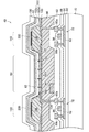
上述したように、有機EL表示装置2の駆動時には各画素のOLED6は映像信号に応じたキャリアを供給されて発光する。図5には当該駆動時にて下部電極100から発光素子層102へ供給されるキャリアである正孔の流れを矢印で模式的に示している。上部電極62は下部電極100より低い電位を印加され、各画素の下部電極100から発光素子層102の下層102dへ供給される正孔は基本的には当該下部電極100とこれに対向配置された上部電極62との間の電界に従い、矢印120で示すように発光素子層102の上層102uへ引き寄せられ当該画素のEMLに注入される。
As described above, when the organic EL display device 2 is driven, the
一方、下部電極100から下層102dに供給された正孔の一部は矢印122で示すように画素開口60の外側へ向けて下層102d内を移動し得る。このキャリア移動が隣接する画素へのリーク電流となると上述した問題を生じる。この点、有機EL表示装置2では発光素子層102の下層102dは画素境界に分断領域112を形成されていることにより、隣接画素へのリーク電流の到達を阻止することができ、リーク電流による隣接画素の発光が防止される。よって、画像の解像度の低下が抑制される。また、分断領域112を発光色が異なる画素間の境界に配置することで、リーク電流による混色が抑制され高い色純度が得られ、好適な色再現性を実現できる。
On the other hand, some of the holes supplied from the
なお、補助層のうち下層102dを構成するものは他の補助層より比較的厚く形成されることが多く、それに伴い下層102d内を移動してリーク電流となるキャリア量が大きくなる。この点、本実施形態では下層102dに分断領域112を設けることで、画素間のリーク電流を好適に抑制することができる。
Of the auxiliary layers, what constitutes the
また、OLED6は白色発光とすることもできる。例えば、白色発光のOLED6は発光色が異なる複数のOLEDを光透過性の中間層を介して電気的に直列接続したタンデム構造とすることができる。タンデム構造では中間層として設けられる電荷発生層(charge generation layer:CGL)もHIL、HTL等と同様、キャリア移動性を有する補助層である。本発明はタンデム構造のOLED6を有する有機EL表示装置2に適用することもできる。この場合も上述の単色発光のOLED6と同様、下部電極100の上に積層されるHTL/HIL層110に分断領域112が設けられ、これにより画素間のリーク電流を好適に抑制することができる。
The
分断領域112は各画素を取り囲む画素境界の全周に沿って配置することができる。すなわち、HTL/HIL層110が分断領域112により画素ごとに分かれた構造とすることができる。
The dividing
また、既に述べたように分断領域112を発光色が互いに異なる隣接画素間の境界に沿って配置することにより好適な色再現性を実現できる。例えば、本実施形態ではRGB画素がストライプ配列され、行方向に隣り合う各画素対は互いに発光色が異なる。この場合、分断領域112を列方向に延びる画素境界に沿って設けることで隣接画素間の混色を防止できる。
Further, as described above, it is possible to realize suitable color reproducibility by arranging the divided
なお、分断領域112は発光色が互いに異なる隣接画素間の境界の全体に沿ってではなく一部のみに沿って形成されてもよい。
The dividing
さて、表示パネル40の製造では、生産効率を高めるために、1枚の大きな基材70上に複数面の表示パネル40を同時に形成する手法が採用される。この製造手法では基材上へのTFTの形成などの工程は複数面の表示パネル40を一体に行われ、一方、OLED形成工程は複数面の表示パネル40を分割して行われる。つまり、この製造方法は、複数面の表示パネル40がつながった状態で加工される前段工程と、表示パネル40ごとに分割されて残りの加工が施される後段工程とに分けられ、ここでは前段工程をTFT工程、後段工程をOLED工程と呼ぶ。
Now, in manufacturing the
TFT工程は基本的に、集積回路などを製造する半導体製造プロセスを利用して行うことができる工程からなり、比較的にプロセス条件の自由度が高く、例えば、数百℃程度の高温プロセスを利用するように製造工程を設計することも可能である。一方、OLED工程は、有機材料からなる発光素子層の劣化を防ぐため、雰囲気温度の上限が数十℃程度に制限され得る。つまり、OLED工程は、表示パネル40をそれぞれ加工することにより工数が増加し、またTFT工程に比べてより確実にプロセス条件を制御する必要がある。そのため、表示パネル40の製造工程においてTFT工程の占める割合を大きくし、OLED工程の占める割合を小さくすることで、表示パネル40の製造コストの低減や製造期間の短縮を図ることができる。
The TFT process basically consists of processes that can be performed using a semiconductor manufacturing process for manufacturing integrated circuits, etc., and has a relatively high degree of freedom in process conditions, for example, using a high-temperature process of about several hundred degrees Celsius. It is also possible to design the manufacturing process in such a way. On the other hand, in the OLED process, the upper limit of the ambient temperature can be limited to about several tens of degrees Celsius in order to prevent deterioration of the light emitting element layer made of an organic material. That is, in the OLED process, man-hours are increased by processing the
本実施形態では、図4(a)に示す構造を形成する工程がTFT工程として行われる。すなわち、基材70の上にTFT72などからなる回路を形成し、その上に平坦化膜96を積層し、また下部電極100及びバンク106が形成される。
In this embodiment, the process of forming the structure shown in FIG. 4A is performed as a TFT process. That is, a circuit composed of the
本実施形態では、さらに発光素子層102の下層102dを形成する工程がTFT工程として行われ、これにより、上に述べた製造コスト低減や製造期間短縮の効果が得られる。つまり、境界領域にバンク106が形成された後、さらにTFT工程において、表示領域42の全面にHTL/HIL層110を形成し(図4(b))、HTL/HIL層110の上にマスク116を形成し、このマスク116を用いて分断領域112を形成する。
In the present embodiment, the process of forming the
なお、OLED工程は発光素子層102の上層102uを形成する工程(図4(d))、上部電極62を形成する工程(図4(e))、及びその後の工程を含む。
The OLED process includes a process of forming the
[第2の実施形態]
以下、本発明の第2の実施形態に係る有機EL表示装置2bを説明する。本実施形態と上記第1の実施形態とは分断領域112の構造及び形成方法に相違点を有し、その他の点では基本的に共通である。以下、第2の実施形態について第1の実施形態との相違点を中心に説明する。
[Second Embodiment]
Hereinafter, an organic EL display device 2b according to a second embodiment of the present invention will be described. The present embodiment and the first embodiment have a difference in the structure and forming method of the dividing
有機EL表示装置2bの表示パネル40の模式的な平面図は、第1の実施形態について示した図2と基本的には同じであり、これを援用する。図5は図2に示すIII−III線に沿った位置での本実施形態の表示パネル40の模式的な垂直断面図である。第1の実施形態の分断領域112は、発光素子層102におけるHTL/HIL層110といったキャリア移動性を有した補助層である下層102dが存在しない領域であった。これに対し、本実施形態の分断領域112は、下層102dにおいてその材料の変質・変性によりキャリア移動性を喪失した領域であり、図5においてバンク106の上の分断領域112には、キャリア移動性を喪失した下層102dである変質層200が存在する。
The schematic plan view of the
例えば、第1の実施形態と同様にして下層102d、及び分断領域112を形成する領域に開口部114を備えたマスク116を形成する(図4(c))。本実施形態では当該マスク116を用いて、例えば、イオン注入やエネルギー線照射を行う。これにより、開口部114の下層102d(HTL/HIL層110)に化学的変化を起こさせたり、分子構造の破壊を起こさせたりすることで、下層102dが有していた導電性を失わせ変質層200を形成する。
For example, the
変質層200を形成した後は、第1の実施形態における有機EL表示装置2と基本的に同様の工程で本実施形態の有機EL表示装置2bが完成される。例えば、変質層200の形成後、まず上層102uを積層して発光素子層102を形成し(図4(d))、次に発光素子層102の上に上部電極62を形成してOLED6が形成される(図4(e))。
After the altered
上記各実施形態ではRGB画素がストライプ配列された有機EL表示装置2にて分断領域112を設けてリーク電流を抑制する構造を説明したが、当該リーク電流抑制構造は他の画素配列においても適用することができる。
In each of the embodiments described above, the structure in which the organic EL display device 2 in which the RGB pixels are arranged in stripes is provided with the dividing
また上記各実施形態及び変形例では、下部電極100がOLED6のアノード、上部電極62がOLED6のカソードである場合を説明した。しかし、本発明は、下部電極100がOLED6のカソード、上部電極62がOLED6のアノードである場合にも適用できる。その場合、発光素子層102における各層の積層順序は上述の構成とは逆転する。例えば、カソードである下部電極100側から順にEIL、ETL、EML、HTL、HILが積層された構造となる。
In each of the above embodiments and modifications, the case where the
本発明の実施形態として上述した有機EL表示装置2,2bを基にして、当業者が適宜設計変更して実施し得る全ての有機EL表示装置も、本発明の要旨を包含する限り、本発明の範囲に属する。また、有機EL表示装置以外の表示装置、例えば発光層として量子ドット素子を採用した量子ドット表示装置等も本発明の範囲に属する。 Based on the organic EL display devices 2 and 2b described above as the embodiments of the present invention, all organic EL display devices that can be implemented by those skilled in the art as appropriate are included in the present invention as long as they include the gist of the present invention. Belongs to the range. In addition, display devices other than organic EL display devices, for example, quantum dot display devices employing quantum dot elements as the light emitting layer, also belong to the scope of the present invention.
本発明の思想の範疇において、当業者であれば、各種の変更例及び修正例に想到し得るものであり、それら変更例及び修正例についても本発明の範囲に属するものと了解される。例えば、前述の各実施形態に対して、当業者が適宜、構成要素の追加、削除若しくは設計変更を行ったもの、又は、工程の追加、省略若しくは条件変更を行ったものも、本発明の要旨を備えている限り、本発明の範囲に含まれる。 In the scope of the idea of the present invention, those skilled in the art can conceive various changes and modifications, and it is understood that these changes and modifications also belong to the scope of the present invention. For example, those in which the person skilled in the art appropriately added, deleted, or changed the design of the above-described embodiments, or those in which the process was added, omitted, or changed the conditions are also included in the gist of the present invention. As long as it is provided, it is included in the scope of the present invention.
また、本実施形態において述べた態様によりもたらされる他の作用効果について本明細書記載から明らかなもの、又は当業者において適宜想到し得るものついては、当然に本発明によりもたらされるものと解される。 In addition, it is understood that other functions and effects brought about by the aspects described in the present embodiment are apparent from the description of the present specification or can be appropriately conceived by those skilled in the art to be brought about by the present invention.
2 有機EL表示装置、4 画素アレイ部、6 OLED、8 画素回路、10 点灯TFT、12 駆動TFT、14 キャパシタ、20 走査線駆動回路、22 映像線駆動回路、24 駆動電源回路、26 基準電源回路、28 制御装置、30 走査信号線、32 映像信号線、34 駆動電源線、40 表示パネル、42 表示領域、44 陰極、46 部品実装領域、48 ドライバIC、50 FPC、60 画素開口、62 上部電極、70 基材、72 TFT、80 下地層、82 半導体領域、84 ゲート絶縁膜、86 ゲート電極、88,92 層間絶縁膜、90a ソース電極、90b ドレイン電極、94 配線、96 平坦化膜、100 下部電極、102 発光素子層、104 コンタクトホール、106 バンク、108 封止膜、110 HTL/HIL層、112 分断領域、200 変質層。
2 organic EL display device, 4 pixel array section, 6 OLED, 8 pixel circuit, 10 lighting TFT, 12 driving TFT, 14 capacitor, 20 scanning line driving circuit, 22 video line driving circuit, 24 driving power supply circuit, 26 reference
Claims (5)
前記各画素に映像信号に応じた量のキャリアを供給する画素電極と、
前記画素の境界に沿って形成されたバンクと、
キャリア輸送層又はキャリア注入層を含むキャリア移動性を有した層であり前記画素電極及び前記バンク上に積層された補助層と当該補助層の上に積層され前記キャリアを注入されて発光する発光層とを含む発光素子層と、
前記発光素子層の上に配置され前記画素電極と共に前記発光素子層に電圧を印加する対向電極と、
を有し、
前記補助層には前記バンク上に分断領域が設けられ、当該分断領域は隣接画素間での前記補助層を介した前記キャリアの移動を阻害すること、
を特徴とする表示装置。 A display device comprising an image display area on a substrate, wherein a plurality of light emitting areas serving as pixels are arranged in the image display area,
A pixel electrode that supplies each pixel with an amount of carriers according to a video signal;
Banks formed along the boundaries of the pixels;
A layer having carrier mobility including a carrier transport layer or a carrier injection layer, an auxiliary layer laminated on the pixel electrode and the bank, and a light emitting layer which is laminated on the auxiliary layer and emits light by injecting the carrier. A light emitting element layer comprising:
A counter electrode disposed on the light emitting element layer and applying a voltage to the light emitting element layer together with the pixel electrode;
Have
The auxiliary layer is provided with a dividing region on the bank, and the dividing region inhibits movement of the carrier through the auxiliary layer between adjacent pixels,
A display device.
前記分断領域は前記補助層のパターニングにおける当該補助層の非形成領域であること、を特徴とする表示装置。 The display device according to claim 1,
The display device according to claim 1, wherein the divided region is a region where the auxiliary layer is not formed in the patterning of the auxiliary layer.
前記分断領域は、当該分断領域に形成された前記補助層の材料の変質により前記キャリア移動性を喪失していること、を特徴とする表示装置。 The display device according to claim 1,
The display device according to claim 1, wherein the divided region loses the carrier mobility due to a change in material of the auxiliary layer formed in the divided region.
前記補助層は、前記分断領域により前記画素ごとに分かれていること、を特徴とする表示装置。 In the display device according to any one of claims 1 to 3,
The display device according to claim 1, wherein the auxiliary layer is divided for each of the pixels by the divided region.
前記画像表示領域は発光色の異なる複数種類の前記画素を含み、
前記分断領域は、前記発光色が異なる隣接した各画素対において当該画素間の境界の少なくとも一部に沿って配置されていること、
を特徴とする表示装置。 In the display device according to any one of claims 1 to 3,
The image display area includes a plurality of types of the pixels having different emission colors,
The divided region is disposed along at least a part of a boundary between the pixels in each adjacent pixel pair having different emission colors;
A display device.
Priority Applications (4)
| Application Number | Priority Date | Filing Date | Title |
|---|---|---|---|
| JP2014240887A JP2016103395A (en) | 2014-11-28 | 2014-11-28 | Display device |
| US14/922,793 US9536933B2 (en) | 2014-11-28 | 2015-10-26 | Display device having a light emitting layer on the auxiliary layer |
| KR1020150165210A KR20160064994A (en) | 2014-11-28 | 2015-11-25 | Display device |
| CN201510849395.7A CN105655377B (en) | 2014-11-28 | 2015-11-27 | Display device |
Applications Claiming Priority (1)
| Application Number | Priority Date | Filing Date | Title |
|---|---|---|---|
| JP2014240887A JP2016103395A (en) | 2014-11-28 | 2014-11-28 | Display device |
Publications (2)
| Publication Number | Publication Date |
|---|---|
| JP2016103395A true JP2016103395A (en) | 2016-06-02 |
| JP2016103395A5 JP2016103395A5 (en) | 2017-12-21 |
Family
ID=56079661
Family Applications (1)
| Application Number | Title | Priority Date | Filing Date |
|---|---|---|---|
| JP2014240887A Pending JP2016103395A (en) | 2014-11-28 | 2014-11-28 | Display device |
Country Status (4)
| Country | Link |
|---|---|
| US (1) | US9536933B2 (en) |
| JP (1) | JP2016103395A (en) |
| KR (1) | KR20160064994A (en) |
| CN (1) | CN105655377B (en) |
Cited By (16)
| Publication number | Priority date | Publication date | Assignee | Title |
|---|---|---|---|---|
| JP2017220528A (en) * | 2016-06-06 | 2017-12-14 | 株式会社Joled | Organic EL display panel |
| CN107863365A (en) * | 2016-08-31 | 2018-03-30 | 乐金显示有限公司 | Organic light-emitting display device and its manufacture method |
| CN108122943A (en) * | 2016-11-30 | 2018-06-05 | 乐金显示有限公司 | Organic electroluminescence display panel |
| JP2019067747A (en) * | 2017-10-03 | 2019-04-25 | Tianma Japan株式会社 | Oled display device and manufacturing method thereof |
| US10720593B2 (en) | 2018-03-06 | 2020-07-21 | Japan Display Inc. | Display device |
| US10840469B2 (en) | 2017-10-03 | 2020-11-17 | Xiamen Tianma Micro-Electronics Co., Ltd. | OLED display device and manufacturing method thereof |
| US10878748B2 (en) | 2018-04-24 | 2020-12-29 | Japan Display Inc. | Display device |
| US10903443B2 (en) | 2018-03-08 | 2021-01-26 | Japan Display Inc. | Organic EL display device |
| WO2021029184A1 (en) * | 2019-08-09 | 2021-02-18 | 株式会社ジャパンディスプレイ | Organic el display device |
| US10937986B2 (en) | 2018-10-23 | 2021-03-02 | Japan Display Inc. | Display device |
| JP2021516843A (en) * | 2018-03-27 | 2021-07-08 | 京東方科技集團股▲ふん▼有限公司Boe Technology Group Co.,Ltd. | Light emitting element and its manufacturing method, display device |
| WO2022059204A1 (en) * | 2020-09-18 | 2022-03-24 | シャープ株式会社 | Light-emitting element |
| WO2022059094A1 (en) * | 2020-09-16 | 2022-03-24 | シャープ株式会社 | Display device manufacturing method and display device |
| US11450828B2 (en) | 2019-12-19 | 2022-09-20 | Japan Display Inc. | Display device |
| US11706951B2 (en) | 2019-09-13 | 2023-07-18 | Japan Display Inc. | OLED including inter-pixel sections having different resistances |
| US11895858B2 (en) | 2020-10-08 | 2024-02-06 | Japan Display Inc. | Display device having organic light emitting diode with low threshold layer |
Families Citing this family (13)
| Publication number | Priority date | Publication date | Assignee | Title |
|---|---|---|---|---|
| KR102418009B1 (en) * | 2015-06-25 | 2022-07-05 | 엘지디스플레이 주식회사 | Organic light emitting display device |
| KR102646658B1 (en) * | 2015-06-30 | 2024-03-12 | 엘지디스플레이 주식회사 | Organic light emitting display device and method of fabricating the same |
| CN106653805A (en) * | 2016-11-29 | 2017-05-10 | 武汉华星光电技术有限公司 | Color mixture-prevention organic light emitting display device and manufacturing method thereof |
| KR20180062291A (en) * | 2016-11-30 | 2018-06-08 | 엘지디스플레이 주식회사 | Organic Light Emitting Display Panel |
| WO2018212960A1 (en) | 2017-05-17 | 2018-11-22 | Apple Inc. | Organic light-emitting diode display with reduced lateral leakage |
| JP2019110271A (en) * | 2017-12-20 | 2019-07-04 | 株式会社ジャパンディスプレイ | Display |
| FR3079909B1 (en) | 2018-04-05 | 2022-10-14 | Microoled | ELECTROLUMINESCENT DEVICE WITH IMPROVED RESOLUTION AND RELIABILITY |
| CN109301078B (en) * | 2018-10-17 | 2022-01-04 | 京东方科技集团股份有限公司 | Display substrate, manufacturing method thereof and display device |
| KR20210049292A (en) * | 2019-10-25 | 2021-05-06 | 엘지디스플레이 주식회사 | Electroluminescent Display Device |
| CN110993678B (en) * | 2019-12-20 | 2022-05-13 | 京东方科技集团股份有限公司 | Display substrate, preparation method thereof and display device |
| WO2023201717A1 (en) * | 2022-04-22 | 2023-10-26 | 京东方科技集团股份有限公司 | Oled device and manufacturing method therefor, and display panel |
| CN114975812B (en) * | 2022-05-07 | 2024-03-01 | 武汉华星光电半导体显示技术有限公司 | Display panel |
| WO2024045105A1 (en) * | 2022-09-01 | 2024-03-07 | 京东方科技集团股份有限公司 | Display substrate, manufacturing method therefor, and display apparatus |
Citations (9)
| Publication number | Priority date | Publication date | Assignee | Title |
|---|---|---|---|---|
| JP2004158436A (en) * | 2002-11-04 | 2004-06-03 | Samsung Sdi Co Ltd | Organic electroluminescent display and its manufacturing method |
| US20040139914A1 (en) * | 2002-08-30 | 2004-07-22 | Semiconductor Energy Laboratory Co., Ltd. | Fabrication system, light-emitting device and fabricating method of organic compound-containing layer |
| JP2005044622A (en) * | 2003-07-22 | 2005-02-17 | Sony Corp | Manufacturing method of organic light emitting element, and manufacturing method of display device |
| JP2005116330A (en) * | 2003-10-07 | 2005-04-28 | Sony Corp | Method of manufacturing organic light emitting element, organic light emitting element and display device |
| JP2007095611A (en) * | 2005-09-30 | 2007-04-12 | Seiko Epson Corp | Display device and electronic equipment, manufacturing method of display device |
| JP2008078590A (en) * | 2006-09-25 | 2008-04-03 | Dainippon Printing Co Ltd | Organic electroluminescence element, and manufacturing method thereof |
| JP2008243559A (en) * | 2007-03-27 | 2008-10-09 | Toppan Printing Co Ltd | Manufacturing method of organic electroluminescent display device |
| JP2009277602A (en) * | 2008-05-16 | 2009-11-26 | Dainippon Printing Co Ltd | Substrate for organic electroluminescent element, the organic electroluminescent element, and their manufacturing method |
| US20140091285A1 (en) * | 2012-09-28 | 2014-04-03 | Hyea-Weon Shin | Organic light emitting display devices and methods of manufacturing organic light emitting display devices |
Family Cites Families (7)
| Publication number | Priority date | Publication date | Assignee | Title |
|---|---|---|---|---|
| KR101325577B1 (en) * | 2006-04-28 | 2013-11-06 | 삼성디스플레이 주식회사 | Organic electro luminescence device and method of manufacturing the same |
| JP2008002311A (en) * | 2006-06-21 | 2008-01-10 | Matsushita Electric Ind Co Ltd | Scroll compressor |
| US7972943B2 (en) * | 2007-03-02 | 2011-07-05 | Semiconductor Energy Laboratory Co., Ltd. | Manufacturing method of semiconductor device |
| KR100994121B1 (en) | 2009-03-11 | 2010-11-15 | 삼성모바일디스플레이주식회사 | Organic light emitting display apparatus |
| JP5677316B2 (en) * | 2010-10-15 | 2015-02-25 | パナソニック株式会社 | ORGANIC LIGHT EMITTING PANEL, ITS MANUFACTURING METHOD, AND ORGANIC DISPLAY DEVICE |
| JP2012155953A (en) | 2011-01-25 | 2012-08-16 | Sony Corp | Organic el display device and electronic apparatus |
| KR102343715B1 (en) * | 2012-07-20 | 2021-12-27 | 가부시키가이샤 한도오따이 에네루기 켄큐쇼 | Semiconductor device and method for manufacturing semiconductor device |
-
2014
- 2014-11-28 JP JP2014240887A patent/JP2016103395A/en active Pending
-
2015
- 2015-10-26 US US14/922,793 patent/US9536933B2/en active Active
- 2015-11-25 KR KR1020150165210A patent/KR20160064994A/en not_active Application Discontinuation
- 2015-11-27 CN CN201510849395.7A patent/CN105655377B/en active Active
Patent Citations (9)
| Publication number | Priority date | Publication date | Assignee | Title |
|---|---|---|---|---|
| US20040139914A1 (en) * | 2002-08-30 | 2004-07-22 | Semiconductor Energy Laboratory Co., Ltd. | Fabrication system, light-emitting device and fabricating method of organic compound-containing layer |
| JP2004158436A (en) * | 2002-11-04 | 2004-06-03 | Samsung Sdi Co Ltd | Organic electroluminescent display and its manufacturing method |
| JP2005044622A (en) * | 2003-07-22 | 2005-02-17 | Sony Corp | Manufacturing method of organic light emitting element, and manufacturing method of display device |
| JP2005116330A (en) * | 2003-10-07 | 2005-04-28 | Sony Corp | Method of manufacturing organic light emitting element, organic light emitting element and display device |
| JP2007095611A (en) * | 2005-09-30 | 2007-04-12 | Seiko Epson Corp | Display device and electronic equipment, manufacturing method of display device |
| JP2008078590A (en) * | 2006-09-25 | 2008-04-03 | Dainippon Printing Co Ltd | Organic electroluminescence element, and manufacturing method thereof |
| JP2008243559A (en) * | 2007-03-27 | 2008-10-09 | Toppan Printing Co Ltd | Manufacturing method of organic electroluminescent display device |
| JP2009277602A (en) * | 2008-05-16 | 2009-11-26 | Dainippon Printing Co Ltd | Substrate for organic electroluminescent element, the organic electroluminescent element, and their manufacturing method |
| US20140091285A1 (en) * | 2012-09-28 | 2014-04-03 | Hyea-Weon Shin | Organic light emitting display devices and methods of manufacturing organic light emitting display devices |
Cited By (22)
| Publication number | Priority date | Publication date | Assignee | Title |
|---|---|---|---|---|
| JP2017220528A (en) * | 2016-06-06 | 2017-12-14 | 株式会社Joled | Organic EL display panel |
| CN107863365A (en) * | 2016-08-31 | 2018-03-30 | 乐金显示有限公司 | Organic light-emitting display device and its manufacture method |
| CN107863365B (en) * | 2016-08-31 | 2022-01-04 | 乐金显示有限公司 | Organic light emitting display device and method of manufacturing the same |
| CN108122943A (en) * | 2016-11-30 | 2018-06-05 | 乐金显示有限公司 | Organic electroluminescence display panel |
| JP2018093196A (en) * | 2016-11-30 | 2018-06-14 | エルジー ディスプレイ カンパニー リミテッド | Organic light emitting display panel |
| CN108122943B (en) * | 2016-11-30 | 2021-12-21 | 乐金显示有限公司 | Organic light emitting display panel |
| US10840469B2 (en) | 2017-10-03 | 2020-11-17 | Xiamen Tianma Micro-Electronics Co., Ltd. | OLED display device and manufacturing method thereof |
| JP7083103B2 (en) | 2017-10-03 | 2022-06-10 | Tianma Japan株式会社 | OLED display device and its manufacturing method |
| JP2019067747A (en) * | 2017-10-03 | 2019-04-25 | Tianma Japan株式会社 | Oled display device and manufacturing method thereof |
| US10720593B2 (en) | 2018-03-06 | 2020-07-21 | Japan Display Inc. | Display device |
| US10903443B2 (en) | 2018-03-08 | 2021-01-26 | Japan Display Inc. | Organic EL display device |
| US11744117B2 (en) | 2018-03-27 | 2023-08-29 | Boe Technology Group Co., Ltd. | Light emitting device and method for manufacturing the same, and display device |
| JP2021516843A (en) * | 2018-03-27 | 2021-07-08 | 京東方科技集團股▲ふん▼有限公司Boe Technology Group Co.,Ltd. | Light emitting element and its manufacturing method, display device |
| JP7182569B2 (en) | 2018-03-27 | 2022-12-02 | 京東方科技集團股▲ふん▼有限公司 | Light-emitting element, manufacturing method thereof, and display device |
| US10878748B2 (en) | 2018-04-24 | 2020-12-29 | Japan Display Inc. | Display device |
| US10937986B2 (en) | 2018-10-23 | 2021-03-02 | Japan Display Inc. | Display device |
| WO2021029184A1 (en) * | 2019-08-09 | 2021-02-18 | 株式会社ジャパンディスプレイ | Organic el display device |
| US11706951B2 (en) | 2019-09-13 | 2023-07-18 | Japan Display Inc. | OLED including inter-pixel sections having different resistances |
| US11450828B2 (en) | 2019-12-19 | 2022-09-20 | Japan Display Inc. | Display device |
| WO2022059094A1 (en) * | 2020-09-16 | 2022-03-24 | シャープ株式会社 | Display device manufacturing method and display device |
| WO2022059204A1 (en) * | 2020-09-18 | 2022-03-24 | シャープ株式会社 | Light-emitting element |
| US11895858B2 (en) | 2020-10-08 | 2024-02-06 | Japan Display Inc. | Display device having organic light emitting diode with low threshold layer |
Also Published As
| Publication number | Publication date |
|---|---|
| KR20160064994A (en) | 2016-06-08 |
| CN105655377A (en) | 2016-06-08 |
| CN105655377B (en) | 2019-03-05 |
| US9536933B2 (en) | 2017-01-03 |
| US20160155785A1 (en) | 2016-06-02 |
Similar Documents
| Publication | Publication Date | Title |
|---|---|---|
| US9536933B2 (en) | Display device having a light emitting layer on the auxiliary layer | |
| US9461100B2 (en) | Display device | |
| JP4206388B2 (en) | Flat panel display device | |
| KR101328979B1 (en) | Organic light emitting display device | |
| JP4507611B2 (en) | ORGANIC ELECTROLUMINESCENCE DEVICE AND ELECTRONIC DEVICE | |
| KR20190092650A (en) | organic light emitting display device and Manufacturing method of the same | |
| KR100740132B1 (en) | Organic light emitting display | |
| US9941338B2 (en) | Organic light-emitting diode display and method of manufacturing the same | |
| KR101864332B1 (en) | Organic light emitting diodes | |
| KR100553745B1 (en) | Flat panel display | |
| JP2005049808A (en) | Flat panel display device | |
| KR20170113866A (en) | Display apparatus | |
| KR20180118857A (en) | Organic light emitting diode display | |
| US20150014639A1 (en) | Organic light emitting diode display having reduced power consumption | |
| US10205113B2 (en) | Organic electroluminescence device including an emissive layer including an assistant dopant layer and light-emitting dopant layer | |
| KR20150098576A (en) | Organic electroluminescent display device | |
| WO2019064574A1 (en) | Display device | |
| JP2019016504A (en) | Display device and method of manufacturing display device | |
| US10559775B2 (en) | Organic EL display device | |
| US10923536B2 (en) | Organic el display device and method of manufacturing organic el display device | |
| US9293740B2 (en) | Method of manufacturing EL display device | |
| JP7126140B2 (en) | Organic EL display device | |
| KR102037487B1 (en) | Method for fabricating Organic Electroluminescence Device and the Organic Electroluminescence Device fabricated by the method | |
| JP2019160392A (en) | Display device | |
| KR100739645B1 (en) | Organic light emitting display |
Legal Events
| Date | Code | Title | Description |
|---|---|---|---|
| A521 | Request for written amendment filed |
Free format text: JAPANESE INTERMEDIATE CODE: A523 Effective date: 20171109 |
|
| A621 | Written request for application examination |
Free format text: JAPANESE INTERMEDIATE CODE: A621 Effective date: 20171109 |
|
| A977 | Report on retrieval |
Free format text: JAPANESE INTERMEDIATE CODE: A971007 Effective date: 20180928 |
|
| A131 | Notification of reasons for refusal |
Free format text: JAPANESE INTERMEDIATE CODE: A131 Effective date: 20181016 |
|
| A02 | Decision of refusal |
Free format text: JAPANESE INTERMEDIATE CODE: A02 Effective date: 20190409 |