KR20160064994A - Display device - Google Patents
Display device Download PDFInfo
- Publication number
- KR20160064994A KR20160064994A KR1020150165210A KR20150165210A KR20160064994A KR 20160064994 A KR20160064994 A KR 20160064994A KR 1020150165210 A KR1020150165210 A KR 1020150165210A KR 20150165210 A KR20150165210 A KR 20150165210A KR 20160064994 A KR20160064994 A KR 20160064994A
- Authority
- KR
- South Korea
- Prior art keywords
- layer
- pixel
- pixels
- region
- bank
- Prior art date
Links
- 238000002347 injection Methods 0.000 claims abstract description 5
- 239000007924 injection Substances 0.000 claims abstract description 5
- 238000000034 method Methods 0.000 claims description 43
- 239000000969 carrier Substances 0.000 claims description 7
- 239000000463 material Substances 0.000 claims description 6
- 230000004075 alteration Effects 0.000 claims description 2
- 239000010410 layer Substances 0.000 description 114
- 239000010408 film Substances 0.000 description 36
- 230000008569 process Effects 0.000 description 25
- 238000005401 electroluminescence Methods 0.000 description 23
- 239000000758 substrate Substances 0.000 description 19
- 238000004519 manufacturing process Methods 0.000 description 13
- 238000007789 sealing Methods 0.000 description 8
- 239000003086 colorant Substances 0.000 description 7
- 230000015572 biosynthetic process Effects 0.000 description 5
- 238000000059 patterning Methods 0.000 description 5
- 238000004544 sputter deposition Methods 0.000 description 5
- 238000005229 chemical vapour deposition Methods 0.000 description 4
- 239000011229 interlayer Substances 0.000 description 4
- 229910052751 metal Inorganic materials 0.000 description 4
- 239000002184 metal Substances 0.000 description 4
- 239000003990 capacitor Substances 0.000 description 3
- 238000012986 modification Methods 0.000 description 3
- 230000004048 modification Effects 0.000 description 3
- 239000011368 organic material Substances 0.000 description 3
- 230000001681 protective effect Effects 0.000 description 3
- 239000011347 resin Substances 0.000 description 3
- 229920005989 resin Polymers 0.000 description 3
- 239000004065 semiconductor Substances 0.000 description 3
- 238000013461 design Methods 0.000 description 2
- 230000006866 deterioration Effects 0.000 description 2
- 238000011161 development Methods 0.000 description 2
- 238000010586 diagram Methods 0.000 description 2
- 230000000694 effects Effects 0.000 description 2
- 239000000945 filler Substances 0.000 description 2
- 239000011521 glass Substances 0.000 description 2
- 239000011810 insulating material Substances 0.000 description 2
- 238000005468 ion implantation Methods 0.000 description 2
- 239000011159 matrix material Substances 0.000 description 2
- 230000036961 partial effect Effects 0.000 description 2
- 238000000206 photolithography Methods 0.000 description 2
- 229920002120 photoresistant polymer Polymers 0.000 description 2
- 239000002096 quantum dot Substances 0.000 description 2
- 230000002829 reductive effect Effects 0.000 description 2
- LIVNPJMFVYWSIS-UHFFFAOYSA-N silicon monoxide Chemical compound [Si-]#[O+] LIVNPJMFVYWSIS-UHFFFAOYSA-N 0.000 description 2
- 238000007740 vapor deposition Methods 0.000 description 2
- 239000004925 Acrylic resin Substances 0.000 description 1
- 229920000178 Acrylic resin Polymers 0.000 description 1
- 229920001609 Poly(3,4-ethylenedioxythiophene) Polymers 0.000 description 1
- 239000004642 Polyimide Substances 0.000 description 1
- 229910052581 Si3N4 Inorganic materials 0.000 description 1
- VYPSYNLAJGMNEJ-UHFFFAOYSA-N Silicium dioxide Chemical compound O=[Si]=O VYPSYNLAJGMNEJ-UHFFFAOYSA-N 0.000 description 1
- BQCADISMDOOEFD-UHFFFAOYSA-N Silver Chemical compound [Ag] BQCADISMDOOEFD-UHFFFAOYSA-N 0.000 description 1
- NIXOWILDQLNWCW-UHFFFAOYSA-N acrylic acid group Chemical group C(C=C)(=O)O NIXOWILDQLNWCW-UHFFFAOYSA-N 0.000 description 1
- 229910052782 aluminium Inorganic materials 0.000 description 1
- XAGFODPZIPBFFR-UHFFFAOYSA-N aluminium Chemical compound [Al] XAGFODPZIPBFFR-UHFFFAOYSA-N 0.000 description 1
- 238000003491 array Methods 0.000 description 1
- 230000000903 blocking effect Effects 0.000 description 1
- 230000015556 catabolic process Effects 0.000 description 1
- 230000001413 cellular effect Effects 0.000 description 1
- 238000004040 coloring Methods 0.000 description 1
- 239000000470 constituent Substances 0.000 description 1
- 230000006378 damage Effects 0.000 description 1
- 230000036425 denaturation Effects 0.000 description 1
- 238000004925 denaturation Methods 0.000 description 1
- 230000005684 electric field Effects 0.000 description 1
- 230000005525 hole transport Effects 0.000 description 1
- 239000012535 impurity Substances 0.000 description 1
- 230000002401 inhibitory effect Effects 0.000 description 1
- 238000010030 laminating Methods 0.000 description 1
- 238000004020 luminiscence type Methods 0.000 description 1
- 239000000203 mixture Substances 0.000 description 1
- 238000001579 optical reflectometry Methods 0.000 description 1
- 150000002894 organic compounds Chemical class 0.000 description 1
- 229920000172 poly(styrenesulfonic acid) Polymers 0.000 description 1
- 229910021420 polycrystalline silicon Inorganic materials 0.000 description 1
- 229920001721 polyimide Polymers 0.000 description 1
- 229920005591 polysilicon Polymers 0.000 description 1
- 238000012545 processing Methods 0.000 description 1
- 230000009467 reduction Effects 0.000 description 1
- 238000000926 separation method Methods 0.000 description 1
- 238000004904 shortening Methods 0.000 description 1
- HQVNEWCFYHHQES-UHFFFAOYSA-N silicon nitride Chemical compound N12[Si]34N5[Si]62N3[Si]51N64 HQVNEWCFYHHQES-UHFFFAOYSA-N 0.000 description 1
- 229910052814 silicon oxide Inorganic materials 0.000 description 1
- 229910052709 silver Inorganic materials 0.000 description 1
- 239000004332 silver Substances 0.000 description 1
- 239000010409 thin film Substances 0.000 description 1
Images
Classifications
-
- H—ELECTRICITY
- H10—SEMICONDUCTOR DEVICES; ELECTRIC SOLID-STATE DEVICES NOT OTHERWISE PROVIDED FOR
- H10K—ORGANIC ELECTRIC SOLID-STATE DEVICES
- H10K59/00—Integrated devices, or assemblies of multiple devices, comprising at least one organic light-emitting element covered by group H10K50/00
- H10K59/10—OLED displays
- H10K59/12—Active-matrix OLED [AMOLED] displays
- H10K59/121—Active-matrix OLED [AMOLED] displays characterised by the geometry or disposition of pixel elements
- H10K59/1213—Active-matrix OLED [AMOLED] displays characterised by the geometry or disposition of pixel elements the pixel elements being TFTs
-
- H01L27/326—
-
- H01L27/3248—
-
- H01L51/5048—
-
- H01L51/5088—
-
- H—ELECTRICITY
- H10—SEMICONDUCTOR DEVICES; ELECTRIC SOLID-STATE DEVICES NOT OTHERWISE PROVIDED FOR
- H10K—ORGANIC ELECTRIC SOLID-STATE DEVICES
- H10K50/00—Organic light-emitting devices
- H10K50/10—OLEDs or polymer light-emitting diodes [PLED]
- H10K50/14—Carrier transporting layers
- H10K50/15—Hole transporting layers
-
- H—ELECTRICITY
- H10—SEMICONDUCTOR DEVICES; ELECTRIC SOLID-STATE DEVICES NOT OTHERWISE PROVIDED FOR
- H10K—ORGANIC ELECTRIC SOLID-STATE DEVICES
- H10K50/00—Organic light-emitting devices
- H10K50/10—OLEDs or polymer light-emitting diodes [PLED]
- H10K50/17—Carrier injection layers
-
- H—ELECTRICITY
- H10—SEMICONDUCTOR DEVICES; ELECTRIC SOLID-STATE DEVICES NOT OTHERWISE PROVIDED FOR
- H10K—ORGANIC ELECTRIC SOLID-STATE DEVICES
- H10K59/00—Integrated devices, or assemblies of multiple devices, comprising at least one organic light-emitting element covered by group H10K50/00
- H10K59/10—OLED displays
- H10K59/12—Active-matrix OLED [AMOLED] displays
- H10K59/122—Pixel-defining structures or layers, e.g. banks
-
- H—ELECTRICITY
- H10—SEMICONDUCTOR DEVICES; ELECTRIC SOLID-STATE DEVICES NOT OTHERWISE PROVIDED FOR
- H10K—ORGANIC ELECTRIC SOLID-STATE DEVICES
- H10K59/00—Integrated devices, or assemblies of multiple devices, comprising at least one organic light-emitting element covered by group H10K50/00
- H10K59/30—Devices specially adapted for multicolour light emission
- H10K59/35—Devices specially adapted for multicolour light emission comprising red-green-blue [RGB] subpixels
-
- H01L2227/32—
Abstract
Description
본 발명은 전압 인가에 의해 발광하는 자발광 소자를 이용한 표시 장치에 관한 것이다.The present invention relates to a display device using a self-luminous element which emits light when a voltage is applied.
표시 장치로서, 유기 일렉트로 루미네센스(electroluminescence:EL) 소자 등의 자발광 소자를 이용한 것의 개발이 진행되고 있다. 유기 일렉트로 루미네센스 소자는 일반적으로 OLED(organic light emitting diode)라 칭해지며, 발광 다이오드의 1종이다. OLED는 유기 화합물을 포함하는 발광층에 캐리어(전자나 정공)가 주입되어 발광한다. OLED는 전압의 인가시에 발광층에 효율적으로 캐리어가 주입되도록, 전극과 발광층 사이 등에, 캐리어 이동성을 가진 보조적인 층을 형성하는 구조를 일반적으로 갖고 있다.As a display device, development using a self-luminous element such as an organic electroluminescence (EL) element is under development. An organic electroluminescence device is generally called an organic light emitting diode (OLED), and is one kind of light emitting diode. The OLED emits light by injecting a carrier (electron or hole) into a light emitting layer containing an organic compound. The OLED generally has a structure in which an auxiliary layer having carrier mobility is formed between the electrode and the light emitting layer so that carriers are efficiently injected into the light emitting layer upon application of a voltage.
예를 들어, 보조적인 층으로서, 애노드와 발광층(emitting layer:EML) 사이에, 정공 수송층(hole transport layer:HTL)이나 정공 주입층(hole injection layer:HIL)이 형성된다. 또한, 캐소드와 발광층 사이에는, 전자 수송층(electron transport layer:ETL)이나 전자 주입층(electron injection layer:EIL)이 형성된다. 이들 보조층은 CVD(chemical vapor deposition)법, 스퍼터법, 증착법 등에 의해, 복수의 화소가 배열된 화상 표시 영역 전체에 걸쳐 공통으로 형성된다.For example, as an auxiliary layer, a hole transport layer (HTL) or a hole injection layer (HIL) is formed between an anode and an emitting layer (EML). Further, an electron transport layer (ETL) or an electron injection layer (EIL) is formed between the cathode and the light emitting layer. These auxiliary layers are formed in common throughout the image display region in which a plurality of pixels are arranged by a CVD (chemical vapor deposition) method, a sputtering method, a vapor deposition method, or the like.
상술한 OLED에 있어서의 HTL, HIL과 같은 캐리어 이동성을 가진 층이 화상 표시 영역에 걸쳐 연속되는 공통층으로서 형성되는 발광 소자를 이용한 표시 장치는, 당해 공통층을 통해 인접하는 화소 간에서의 캐리어의 리크가 발생할 수 있다. 인접 화소로의 리크 전류는 당해 인접 화소의 의도하지 않은 발광을 초래한다고 하는 문제가 있었다. 구체적으로는, 리크 전류는 화상의 해상도의 열화를 발생시키는 것 외에, 발광색이 다른 화소 간에 있어서의 리크 전류는 색 재현성(색 순도)의 저하를 발생시킨다고 하는 문제가 있었다. 특히, 화소 사이즈의 축소에 의한 고정밀화에 수반하여 인접 화소의 개구부(또는 발광 영역)가 접근됨으로써 당해 문제가 현저해진다.The display device using the light emitting element in which the layer having the carrier mobility such as HTL and HIL in the above-described OLED is formed as a continuous common layer over the image display region, Leakage may occur. There has been a problem that a leak current to the adjacent pixel causes unintended emission of the adjacent pixel. Specifically, the leakage current causes deterioration of the resolution of the image. In addition, there is a problem that the leakage current between pixels having different emission colors causes a decrease in color reproducibility (color purity). Particularly, as the aperture (or the light emitting region) of the adjacent pixel is approached in association with the high definition by reduction of the pixel size, the problem becomes remarkable.
본 발명은 상기 문제점을 해결하기 위해 이루어진 것으로, 인접하는 화소의 자발광 소자로의 리크 전류가 억제되어, 인접 화소의 의도하지 않은 발광이 방지되는 표시 장치를 제공하는 것을 목적으로 한다.SUMMARY OF THE INVENTION It is an object of the present invention to provide a display device in which leakage current to adjacent self-luminous elements is suppressed and unintended emission of adjacent pixels is prevented.
본 발명에 관한 표시 장치는, 복수의 화소와, 상기 복수의 화소의 각각에 형성된 화소 전극과, 상기 복수의 화소의 경계에 위치하고, 상기 화소 전극의 일부를 노출시키는 뱅크와, 캐리어 수송층과 캐리어 주입층 중 적어도 하나를 포함하고, 상기 화소 전극 상 및 상기 뱅크 상에 적층되어 있는 보조층과, 상기 보조층 상에 적층되어 있는 발광층과, 상기 발광층 상에 위치하고, 상기 복수의 화소에 걸쳐 배치되어 있는 대향 전극을 갖는다. 본 발명에 관한 표시 장치에 있어서, 상기 보조층에는 상기 뱅크 상에 분단 영역이 형성되고, 상기 분단 영역은, 상기 보조층의 상기 분단 영역과는 다른 영역보다도 캐리어의 이동도가 작다. 다른 본 발명에 관한 표시 장치에 있어서의 상기 보조층은, 상기 뱅크의 상면에서 분단되어, 상기 복수의 화소의 각각에 대응하여 배치되어 있다.A display device according to the present invention includes a plurality of pixels, pixel electrodes formed on each of the plurality of pixels, a bank which is located at a boundary between the plurality of pixels and which exposes a part of the pixel electrodes, And an auxiliary layer stacked on the pixel electrode and the bank, a light emitting layer stacked on the auxiliary layer, and a light emitting layer disposed on the light emitting layer and arranged over the plurality of pixels And has an opposite electrode. In the display device according to the present invention, the auxiliary layer is provided with a divided area on the bank, and the divisional area has a smaller mobility of carriers than the divided area of the auxiliary layer. In the display device according to another aspect of the present invention, the auxiliary layer is divided from the upper surface of the bank and arranged corresponding to each of the plurality of pixels.
도 1은 본 발명의 실시 형태에 관한 유기 EL 표시 장치의 개략의 구성을 도시하는 모식도이다.
도 2는 본 발명의 실시 형태에 관한 유기 EL 표시 장치의 표시 패널의 모식적인 평면도이다.
도 3은 본 발명의 제1 실시 형태에 관한 표시 패널의 도 2에 도시하는 Ⅲ-Ⅲ 선을 따른 위치에서의 모식적인 수직 단면도이다.
도 4a-도 4e는 OLED(6)를 형성할 때의 주요한 공정에 있어서의 TFT 기판의 부분 단면도이다.
도 5는 본 발명의 제2 실시 형태에 관한 표시 패널의 도 2에 도시하는 Ⅲ-Ⅲ 선을 따른 위치에서의 모식적인 수직 단면도이다.1 is a schematic diagram showing a schematic configuration of an organic EL display device according to an embodiment of the present invention.
2 is a schematic plan view of a display panel of an organic EL display device according to an embodiment of the present invention.
Fig. 3 is a schematic vertical cross-sectional view of the display panel according to the first embodiment of the present invention at a position along the line III-III shown in Fig.
Figs. 4A to 4E are partial cross-sectional views of the TFT substrate in the main process of forming the
5 is a schematic vertical cross-sectional view of the display panel according to the second embodiment of the present invention at a position along the line III-III shown in FIG.
이하, 본 발명의 실시 형태(이하 실시 형태라 함)에 대해, 도면에 기초하여 설명한다.DESCRIPTION OF THE PREFERRED EMBODIMENTS Hereinafter, embodiments of the present invention (hereinafter referred to as embodiments) will be described with reference to the drawings.
또한, 개시는 어디까지나 일례에 지나지 않으며, 당업자에 있어서, 발명의 주지를 유지한 적절한 변경에 대해 용이하게 상도할 수 있는 것에 대해서는, 당연히 본 발명의 범위에 포함되는 것이다. 또한, 도면은 설명을 보다 명확히 하기 위해, 실제의 형태에 비해, 각 부의 폭, 두께, 형상 등에 대해 모식적으로 표현되는 경우가 있지만, 어디까지나 일례이며, 본 발명의 해석을 한정하는 것은 아니다. 또한, 본 명세서와 각 도면에 있어서, 기출된 도면에 관해 전술한 것과 마찬가지의 요소에는, 동일한 부호를 부여하고, 상세한 설명을 적절히 생략하는 경우가 있다.It is to be understood that the disclosure is by way of example only and that those skilled in the art will readily perceive any suitable modifications that maintain the gist of the invention as a matter of course included within the scope of the present invention. In addition, for the sake of clarity, the drawings are schematically illustrated with respect to the width, thickness, shape, and the like of each part, as compared with the actual shape, but are merely examples and do not limit the interpretation of the present invention. In the present specification and the drawings, the same reference numerals are given to the same elements as those described above in connection with the drawings, and the detailed description may be omitted appropriately.
이하에 설명하는 각 실시 형태의 표시 장치는 유기 EL 표시 장치이다. 유기 EL 표시 장치는, 액티브 매트릭스형 표시 장치이며, 텔레비전, 퍼스널 컴퓨터, 휴대 단말기, 휴대 전화 등에 탑재된다.The display device of each embodiment described below is an organic EL display device. The organic EL display device is an active matrix type display device and is mounted on a television, a personal computer, a portable terminal, a cellular phone, or the like.
표시 장치의 화상 표시 영역에는, 화상을 구성하는 복수의 화소가 2차원 배열된다. 여기서, 화상에 대응하는 2차원의 직교 좌표계 중 하나의 좌표축을 따른 방향을 행 방향, 또 하나의 좌표축을 따른 방향을 열 방향이라 한다. 이후의 설명에서는, 행 방향, 열 방향은 기본적으로는 화상의 수평 방향, 수직 방향으로 하지만, 이것은 편의적인 정의이다. 예를 들어, 동일한 화상 표시 영역에서 화상의 종횡을 전환하여 표시할 수 있는 표시 장치에서는, 화상 표시 영역의 행 방향, 열 방향은 각각 화상의 수직 방향, 수평 방향으로 되는 경우가 있다. 또한, 표시 장치의 구조 자체도, 이하에 설명하는 것에 대해 행 방향과 열 방향을 교체한 것으로 할 수 있다.In the image display area of the display device, a plurality of pixels constituting an image are two-dimensionally arranged. Here, a direction along one coordinate axis of a two-dimensional orthogonal coordinate system corresponding to an image is referred to as a row direction, and a direction along another coordinate axis is referred to as a column direction. In the following description, the row direction and the column direction are basically horizontal and vertical directions of the image, but this is a convenience definition. For example, in a display device capable of switching the vertical and horizontal directions of an image in the same image display area, the row direction and the column direction of the image display area may be the vertical direction and the horizontal direction of the image, respectively. Further, the structure of the display device itself may be replaced with a row direction and a column direction in the following description.
또한, 이하의 실시 형태에서는, 화상 표시 영역에는 발광색이 서로 다른 복수 종류의 화소(서브 픽셀)가 배열되어 컬러 화상을 표시 가능한 표시 장치를 설명한다. 또한, 컬러 화상에 있어서의 화소는, 표시 장치에 있어서의 복수 종류의 서브 픽셀을 포함하는 1세트의 서브 픽셀에 대응하지만, 표시 장치에서는 서브 픽셀이 구성상의 단위이며, 예를 들어, 서브 픽셀마다 OLED나 화소 회로가 형성된다. 따라서 이하의 설명에서는, 기본적으로 서브 픽셀을 화소로 취급한다.In the following embodiments, a display device capable of displaying a color image by arranging a plurality of kinds of pixels (sub-pixels) having different luminescent colors in an image display area will be described. The pixel in the color image corresponds to a set of subpixels including a plurality of kinds of subpixels in the display device, but in the display device, the subpixel is a constituent unit, and for example, every subpixel An OLED or a pixel circuit is formed. Therefore, in the following description, subpixels are basically handled as pixels.
(제1 실시 형태)(First Embodiment)
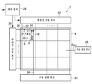
도 1은 실시 형태에 관한 유기 EL 표시 장치(2)의 개략의 구성을 도시하는 모식도이다. 유기 EL 표시 장치(2)는, 화상을 표시하는 화소 어레이부(4)와, 당해 화소 어레이부를 구동하는 구동부를 구비한다. 유기 EL 표시 장치(2)는 유리 기판이나 가요성을 가진 수지 필름 등을 포함하는 기재 상에 박막 트랜지스터(thin film transistor:TFT)나 OLED 등의 적층 구조를 형성하고 있다.1 is a schematic diagram showing a schematic configuration of an organic
화소 어레이부(4)에는 화소에 대응하여 OLED(6) 및 화소 회로(8)가 매트릭스 형상으로 배치된다. 화소 회로(8)는 TFT(10, 12)나 캐패시터(14)로 구성된다.In the
한편, 구동부는 주사선 구동 회로(20), 영상선 구동 회로(22), 구동 전원 회로(24), 기준 전원 회로(26) 및 제어 장치(28)를 포함하고, 화소 회로(8)를 구동하여 OLED(6)의 발광을 제어하는 등의 기능을 한다.The driving section includes a scanning
주사선 구동 회로(20)는 화소의 수평 방향의 배열(화소 행)마다 설치된 주사 신호선(30)에 접속되어 있다. 주사선 구동 회로(20)는 제어 장치(28)로부터 입력되는 타이밍 신호에 따라 주사 신호선(30)을 순서대로 선택하고, 선택한 주사 신호선(30)에, 점등 TFT(10)를 온시키는 전압을 인가한다.The scanning
영상선 구동 회로(22)는 화소의 수직 방향의 배열(화소 열)마다 설치된 영상 신호선(32)에 접속되어 있다. 영상선 구동 회로(22)는 제어 장치(28)로부터 영상 신호를 입력하고, 주사선 구동 회로(20)에 의한 주사 신호선(30)의 선택에 맞추어, 선택된 화소 행의 영상 신호에 따른 전압을 각 영상 신호선(32)으로 출력한다. 당해 전압은, 선택된 화소 행에서 점등 TFT(10)를 통해 캐패시터(14)에 기입된다. 구동 TFT(12)는 기입된 전압에 따른 전류를 OLED(6)에 공급하고, 이에 의해, 선택된 주사 신호선(30)에 대응하는 화소의 OLED(6)가 발광한다.The video
구동 전원 회로(24)는 화소 열마다 설치된 구동 전원선(34)에 접속되고, 구동 전원선(34) 및 선택된 화소 행의 구동 TFT(12)를 통해 OLED(6)에 전류를 공급한다.The driving
기준 전원 회로(26)는, OLED(6)의 캐소드 전극을 구성하는 공통 전극(도시하지 않음)에 정전위 φREF를 부여한다. φREF는 예를 들어, 접지 전위 GND(0V)로 설정할 수 있다.The reference
본 실시 형태에 있어서 OLED(6)의 하부 전극은 화소마다 형성된 화소 전극이며, OLED(6)의 상부 전극이 화소 전극에 대향 배치된 대향 전극으로 된다. 하부 전극은 구동 TFT(12)에 접속된다. 한편, 상부 전극은 전체 화소의 OLED(6)에 공통의 전극으로 구성된다. 본 실시 형태에서는 하부 전극이 OLED(6)의 양극(애노드)이며, 상부 전극이 음극(캐소드)이다.In the present embodiment, the lower electrode of the
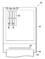
도 2는 유기 EL 표시 장치(2)의 표시 패널(40)의 모식적인 평면도이다. 표시 패널(40)의 표시 영역(42)에 도 1에 도시한 화소 어레이부(4)가 설치되고, 상술한 바와 같이 화소 어레이부(4)에는 OLED가 배열된다. 직사각형인 표시 패널(40)의 한 변에는 부품 실장 영역(46)이 형성되고, 표시 영역(42)에 연결되는 배선이 배치된다. 또한 부품 실장 영역(46)에는 구동부를 구성하는 드라이버 IC(48)가 탑재되거나, FPC(50)가 접속되거나 한다. FPC(50)는 제어 장치(28)나 그 밖의 회로(20, 22, 24, 26) 등에 접속되거나, 그 위에 IC가 탑재되거나 한다.Fig. 2 is a schematic plan view of the
본 실시 형태의 표시 패널(40)은 컬러 화상을 표시하고, 컬러 화상에 있어서의 화소는 예를 들어, 적색(R), 녹색(G) 및 청색(B)에 대응하는 광을 출사하는 화소(서브 픽셀)로 구성된다.The
본 실시 형태에서는 R 화소(52r), G 화소(52g), B 화소(52b)가 표시 영역에 스트라이프 배열되는 예를 설명한다. 당해 배열에서는, 화상의 수직 방향으로 동일한 종류(색)의 화소가 배열되고, 수평 방향으로 RGB가 주기적으로 배열된다. 또한, 도 2에 있어서 R 화소(52r), G 화소(52g), B 화소(52b)는 각각 유효한 발광 영역을 모식적으로 도시하고 있고, 구조상으로는 화소 개구(60)에 대응하고, 그들 사이의 영역은 뱅크에 대응하고 있다.In the present embodiment, an example in which the
표시 패널(40)은 예를 들어, TFT 기판과 대향 기판을, 사이에 충전재를 끼워 접합한 구조로 된다. TFT 기판에는 TFT(72) 등을 포함하는 회로나 OLED(6) 등이 형성된다. 대향 기판에는 편광판이나 터치 패널이 설치될 수 있다. 또한 표시 패널(40)의 컬러화 방식이 컬러 필터 방식인 경우, 예를 들어, 대향 기판에는 컬러 필터가 형성되고, OLED(6)에서 백색광을 생성하고, 당해 백색광을 컬러 필터를 통과시킴으로써 RGB 각 색을 얻는다.The
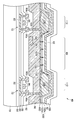
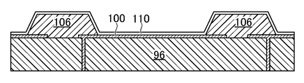
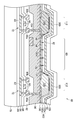
도 3은 도 2에 도시하는 Ⅲ-Ⅲ 선을 따른 위치에서의 표시 패널(40)의 모식적인 수직 단면도이다. 도 3은 상술한 TFT 기판의 단면 구조를 도시하고 있고, 이 위에 형성되는 충전재층과 대향 기판의 구조는 도시를 생략하고 있다. 본 실시 형태에 있어서 화소 어레이부(4)는 톱 에미션형이며, TFT 기판 상에 형성된 OLED(6)에서 발생한 광을 대향 기판으로부터 출사한다. 즉, 도 3에 있어서 OLED(6)의 광은 상향으로 출사된다.3 is a schematic vertical cross-sectional view of the
TFT 기판의 구조는 유리나 수지 필름을 포함하는 기재(70) 상에 각종 층을 적층하고, 또한 패터닝함으로써 형성된다.The structure of the TFT substrate is formed by laminating and patterning various layers on a
구체적으로는 기재(70) 상에 질화 실리콘(SiNy)이나 산화 실리콘(SiOx) 등의 무기 절연 재료를 포함하는 하지층(80)을 통해 폴리실리콘(p-Si)막이 형성되고, 당해 p-Si막을 패터닝하여, 회로층에서 이용하는 개소의 p-Si막을 선택적으로 남긴다. 예를 들어, p-Si막을 이용하여 톱 게이트형의 TFT(72)의 채널부 및 소스·드레인부로 되는 반도체 영역(82)이 형성된다. TFT(72)의 채널부 상에는 게이트 절연막(84)을 통해 게이트 전극(86)이 배치된다. 게이트 전극(86)은 스퍼터링 등에 의해 형성한 금속막을 패터닝하여 형성된다. 이후, 게이트 전극(86)을 덮는 층간 절연막(88)을 적층한다. TFT(72)의 소스부, 드레인부로 되는 p-Si에는 이온 주입에 의해 불순물이 도입되고, 또한 그들 p-Si에 전기적으로 접속된 소스 전극(90a) 및 드레인 전극(90b)이 형성된다. 이와 같이 하여 TFT(72)를 형성한 후, 층간 절연막(92)을 적층한다. 층간 절연막(92)의 표면에는, 스퍼터링 등에 의해 형성한 금속막을 패터닝하여 배선(94) 등을 형성할 수 있고, 당해 금속막과 게이트 전극(86), 소스 전극(90a) 및 드레인 전극(90b)의 형성에 이용한 금속막으로 예를 들어, 도 1에 도시한 주사 신호선(30), 영상 신호선(32), 구동 전원선(34)을 다층 배선 구조로 형성할 수 있다. 이 위에 예를 들어, 아크릴 수지 등의 유기 재료를 적층하여 평탄화막(96)이 형성되고, 이에 의해 평탄화된 표시 영역(42)의 표면에 OLED(6)가 형성된다.Specifically, a polysilicon (p-Si) film is formed on the
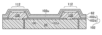
OLED(6)는 하부 전극(100), 발광 소자층(102) 및 상부 전극(62)으로 구성되고, 이들 하부 전극(100), 발광 소자층(102) 및 상부 전극(62)은 기재(70)측으로부터 순서대로 적층된다.The
도 3에 도시하는 TFT(72)가 n채널을 가진 구동 TFT(12)라고 하면, 하부 전극(100)은 TFT(72)의 소스 전극(90a)에 접속된다. 구체적으로는, 상술한 평탄화막(96)의 형성 후, 하부 전극(100)을 TFT(72)에 접속시키기 위한 콘택트 홀(104)이 형성되고, 평탄화막(96) 표면 및 콘택트 홀(104) 내에 형성된 도전체막을 패터닝하여, TFT(72)에 접속된 하부 전극(100)이 화소마다 분리되어 형성된다.3, the
예를 들어, 하부 전극(100)은 ITO, IZO 등으로 형성된다. 또한, 본 실시 형태는 톱 에미션형이므로, 하부 전극(100)은 광 반사율이 높은 재료로 형성된 반사층 상에 투명 도전막을 적층한 구조로 할 수 있다. 예를 들어, 반사층은 알루미늄(Al)이나 은(Ag) 등으로 형성할 수 있고, 발광층으로부터의 광을 표시면, 즉 상부 전극(62)측으로 반사시킨다.For example, the
상술한 바와 같이, 구동 TFT(12)는 각 화소의 영상 신호에 따라 OLED(6)에 흐르는 전류를 제어하고, 하부 전극(100)은 각 화소의 영상 신호에 따른 양의 캐리어를 발광 소자층(102)으로 공급한다. 구체적으로는 본 실시 형태에서는 하부 전극(100)은 애노드이며, 캐리어로서 정공이 하부 전극(100)으로부터 발광 소자층(102)으로 공급된다.As described above, the driving
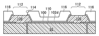
도 4a∼도 4e는 각각, OLED(6)를 형성할 때의 주요한 공정에 있어서의 TFT 기판의 부분 단면도이며, 이들 도면은 하부 전극(100)의 형성 후의 표시 패널(40)의 제조 공정의 개략의 프로세스 플로우를 도시하고 있다. 이하, 도 4a∼도 4e를 참조하여 OLED(6)의 형성 공정을 설명한다.4A to 4E are partial cross-sectional views of the TFT substrate in the main process of forming the
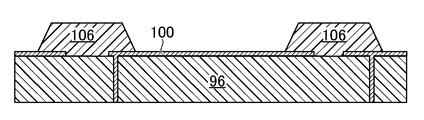
하부 전극(100)의 형성 후, 뱅크(106)를 형성한다(도 4a). 뱅크(106)는 예를 들어, 아크릴, 폴리이미드 등의 감광성 수지를 포토리소그래피 기술이나 잉크젯 방식으로 패터닝하여 화소 경계에 형성되어 하부 전극(100) 사이를 전기적으로 분리한다. 또한, 뱅크(106)는 SiNy나 SiOx 등의 무기 절연 재료로 형성할 수도 있다. 뱅크(106)로 둘러싸인 영역이 도 2에 도시하는 화소 개구(60)로 되고, 당해 영역에는 하부 전극(100)이 노출된다.After the
뱅크(106)의 형성 후, 발광 소자층(102)을 구성하는 각 층이 하부 전극(100) 상에 순서대로 적층된다. 발광 소자층(102)은 캐리어가 주입되어 발광하는 발광층(EML) 및 발광층으로 효율적으로 캐리어를 공급하는 기능을 하는 보조층을 포함한다. 발광 소자층(102)은 보조층으로서 HIL 및 HTL 중 적어도 한쪽을 포함한다.After the formation of the
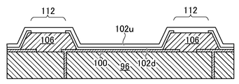
예를 들어, OLED(6)는 RGB 화소 각각의 발광색에 대응한 단색 발광의 OLED이며, 애노드인 하부 전극(100)측으로부터 순서대로 HIL, HTL, EML, ETL이 적층된 구조이다. 당해 구조에서는 HIL, HTL 및 ETL이 보조층이다. 이 중 HIL 및 HTL은 정공을 공급하는 애노드[하부 전극(100)]와 EML 사이에 형성된다. 도 3에서는 발광 소자층(102)을 HIL 및 HTL을 포함하는 하층(102d)과 EML 및 ETL을 포함하는 상층(102u)으로 나누어 도시하고 있다.For example, the
뱅크(106)의 형성 후, 우선, 하층(102d)이 형성된다. 하층(102d)을 구성하는 HTL/HIL은 예를 들어, 폴리(3, 4-에틸렌디옥시티오펜)-폴리(스티렌술폰산)(PEDOT-PSS)나 그 밖의 도전성 유기 재료로 형성된다. 뱅크(106)가 형성된 표시 영역(42)의 표면의 전체에 걸쳐 HTL/HIL층(110)이 예를 들어, 스퍼터링이나 CVD에 의해 성막된다(도 4b).After forming the
그 후, 뱅크(106) 상에 HTL/HIL층(110)의 분단 영역(112)이 형성되고(도 4c), 남는 영역의 HTL/HIL층(110)이 발광 소자층(102)의 하층(102d)으로 된다(도 4d, 도 4e). 분단 영역(112)은 인접 화소 간에서의 HTL/HIL층(110)을 통한 캐리어의 이동을 저해하는 기능을 갖는다. 도면에 도시하는 바와 같이, 분단 영역(112)의 폭은 뱅크(106)의 폭의 일부분으로 충분하고, 하층(102d)의 테두리는 뱅크(106)의 표면에 오버랩시킬 수 있다.4C), and the HTL /
본 실시 형태에서는, 분단 영역(112)은 HTL/HIL층(110)의 비형성 영역이다. 예를 들어, 포토리소그래피 기술을 이용한 패터닝에 의해 HTL/HIL층(110)을 제거함으로써 분단 영역(112)이 형성된다. 구체적으로는, HTL/HIL층(110)의 표면에 포토레지스트막을 성막하고, 당해 포토레지스트막을 이용하여 분단 영역(112)을 형성하는 영역에 개구부(114)를 구비한 마스크(116)를 형성한다. 그리고, 당해 마스크(116)를 이용하여, 개구부(114)로부터 HTL/HIL층(110)을 에칭 제거한다(도 4c).In this embodiment, the dividing
또한, 하층(102d)으로서, 인쇄법 등으로 처음부터 분단 영역(112)을 구비한 패턴을 가진 HTL/HIL층(110)을 형성할 수도 있다.As the
다음으로 하층(102d) 상에 EML, ETL이 표시 영역(42) 전체에 걸쳐 성막되어, 상층(102u)이 형성된다(도 4d). 예를 들어, 상층(102u)은 증착에 의해 형성된다. 또한, 단색 발광의 OLED에 있어서는 EML은 발광색 마다 다른 유기 발광 재료로 형성된다. 이 경우, EML은 잉크젯법 등으로 형성할 수도 있다.Next, EML and ETL are formed over the
하층(102d) 및 상층(102u)을 포함하는 발광 소자층(102) 상에 상부 전극(62)이 예를 들어, 스퍼터링에 의해 성막된다(도 4e). 상부 전극(62)은 기본적으로 표시 영역(42) 전체에 걸쳐 공통으로 형성된다.The
이와 같이 하여 OLED(6)가 형성된다. 또한, 상부 전극(62) 표면에는 도 3에 도시하는 바와 같이 밀봉막(108)이 형성된다. 밀봉막(108)은, 수분 등의 투과를 저지하여, OLED(6)를 보호하는 기능을 갖는다. 밀봉막(108)으로서 예를 들어, SiNy막이 CVD법에 의해 성막된다.Thus, the
또한, TFT 기판에 대향 기판을 접합하지 않는 구조로 할 수도 있고, 이 경우에는 TFT 기판의 표면의 기계적인 강도를 확보하기 위해, 밀봉막(108)의 위 내지 아래, 또는 양쪽에 보호막을 형성할 수 있다. 보호막이 아래에 형성되는 경우에는, 당해 보호막에 뱅크(106)에 의해 발생하는 요철을 평탄화시키는 효과를 갖도록 하여, 밀봉막(108)의 요철을 저감시켜도 된다. 이에 의해 밀봉막의 내부 응력을 저감시킬 수 있어, 밀봉막이 박리되기 어려운 구조로 할 수 있다.In addition, in this case, in order to secure the mechanical strength of the surface of the TFT substrate, a protective film is formed on the upper side, the lower side, or both sides of the sealing
상술한 바와 같이, 유기 EL 표시 장치(2)의 구동시에는 각 화소의 OLED(6)는 영상 신호에 따른 캐리어가 공급되어 발광한다. 도 5에는 당해 구동시에 하부 전극(100)으로부터 발광 소자층(102)으로 공급되는 캐리어인 정공의 흐름을 화살표로 모식적으로 나타내고 있다. 상부 전극(62)은 하부 전극(100)보다 낮은 전위가 인가되고, 각 화소의 하부 전극(100)으로부터 발광 소자층(102)의 하층(102d)으로 공급되는 정공은 기본적으로는 당해 하부 전극(100)과 이것에 대향 배치된 상부 전극(62) 사이의 전계에 따라서, 화살표(120)로 나타내는 바와 같이 발광 소자층(102)의 상층(102u)으로 끌어당겨져 당해 화소의 EML에 주입된다.As described above, in the driving of the organic
한편, 하부 전극(100)으로부터 하층(102d)에 공급된 정공의 일부는 화살표(122)로 나타내는 바와 같이 화소 개구(60)의 외측을 향해 하층(102d) 내를 이동할 수 있다. 이 캐리어 이동이 인접하는 화소로의 리크 전류로 되면 상술한 문제를 발생시킨다. 이 점에서, 유기 EL 표시 장치(2)에서는 발광 소자층(102)의 하층(102d)은 화소 경계에 분단 영역(112)이 형성되어 있음으로써, 인접 화소로의 리크 전류의 도달을 저지할 수 있어, 리크 전류에 의한 인접 화소의 발광이 방지된다. 따라서, 화상의 해상도의 저하가 억제된다. 또한, 분단 영역(112)을 발광색이 다른 화소 간의 경계에 배치함으로써, 리크 전류에 의한 혼색이 억제되어 높은 색 순도가 얻어지고, 적합한 색 재현성을 실현할 수 있다.On the other hand, a part of the holes supplied from the
또한, 보조층 중 하층(102d)을 구성하는 것은 다른 보조층보다 비교적 두껍게 형성되는 경우가 많고, 그것에 수반하여 하층(102d) 내를 이동하여 리크 전류로 되는 캐리어량이 커진다. 이 점에서, 본 실시 형태에서는 하층(102d)에 분단 영역(112)을 형성함으로써, 화소 간의 리크 전류를 적절하게 억제할 수 있다.In addition, the
또한, OLED(6)는 백색 발광으로 할 수도 있다. 예를 들어, 백색 발광의 OLED(6)는 발광색이 다른 복수의 OLED를 광투과성의 중간층을 개재시켜 전기적으로 직렬 접속한 탠덤 구조로 할 수 있다. 탠덤 구조에서는 중간층으로서 형성되는 전하 발생층(charge generation layer:CGL)도 HIL, HTL 등과 마찬가지로, 캐리어 이동성을 갖는 보조층이다. 본 발명은 탠덤 구조의 OLED(6)를 갖는 유기 EL 표시 장치(2)에 적용할 수도 있다. 이 경우도 상술한 단색 발광의 OLED(6)와 마찬가지로, 하부 전극(100) 상에 적층되는 HTL/HIL층(110)에 분단 영역(112)이 형성되고, 이에 의해 화소 간의 리크 전류를 적절하게 억제할 수 있다.Further, the
분단 영역(112)은 각 화소를 둘러싸는 화소 경계의 전체 둘레를 따라 배치할 수 있다. 즉, HTL/HIL층(110)이 분단 영역(112)에 의해 화소마다 나뉘어진 구조로 할 수 있다.The dividing
또한, 이미 설명한 바와 같이 분단 영역(112)을 발광색이 서로 다른 인접 화소 간의 경계를 따라 배치함으로써 적합한 색 재현성을 실현할 수 있다. 예를 들어, 본 실시 형태에서는 RGB 화소가 스트라이프 배열되고, 행 방향으로 인접하는 각 화소 쌍은 서로 발광색이 다르다. 이 경우, 분단 영역(112)을 열 방향으로 연장하는 화소 경계를 따라 형성함으로써 인접 화소 간의 혼색을 방지할 수 있다.In addition, as described above, appropriate color reproducibility can be realized by disposing the dividing
또한, 분단 영역(112)은 발광색이 서로 다른 인접 화소 간의 경계의 전체를 따라서가 아니라 일부만을 따라서 형성되어도 된다.In addition, the dividing
그런데, 표시 패널(40)의 제조에서는, 생산 효율을 높이기 위해, 1매의 큰 기재(70) 상에 복수 면의 표시 패널(40)을 동시에 형성하는 방법이 채용된다. 이 제조 방법에서는 기재 상에의 TFT의 형성 등의 공정은 복수 면의 표시 패널(40)을 일체로 하여 행해지고, 한편, OLED 형성 공정은 복수 면의 표시 패널(40)을 분할하여 행해진다. 즉, 이 제조 방법은, 복수 면의 표시 패널(40)이 연결된 상태에서 가공되는 전단 공정과, 표시 패널(40) 마다 분할되어 나머지의 가공이 실시되는 후단 공정으로 나뉘고, 여기에서는 전단 공정을 TFT 공정, 후단 공정을 OLED 공정이라 칭한다.Incidentally, in the manufacture of the
TFT 공정은 기본적으로, 집적 회로 등을 제조하는 반도체 제조 프로세스를 이용하여 행할 수 있는 공정을 포함하고, 비교적 프로세스 조건의 자유도가 높고, 예를 들어, 수백℃ 정도의 고온 프로세스를 이용하도록 제조 공정을 설계하는 것도 가능하다. 한편, OLED 공정은, 유기 재료를 포함하는 발광 소자층의 열화를 방지하기 위해, 분위기 온도의 상한이 수십℃ 정도로 제한될 수 있다. 즉, OLED 공정은, 복수 면의 표시 패널(40)을 각각 가공함으로써 공정 수가 증가하고, 또한 TFT 공정에 비해 보다 확실하게 프로세스 조건을 제어할 필요가 있다. 그로 인해, 표시 패널(40)의 제조 공정에 있어서 TFT 공정이 차지하는 비율을 크게 하고, OLED 공정이 차지하는 비율을 작게 함으로써, 표시 패널(40)의 제조 비용의 저감이나 제조 기간의 단축을 도모할 수 있다.The TFT process basically includes a process that can be performed by using a semiconductor manufacturing process for manufacturing an integrated circuit and the like. The TFT process has a relatively high degree of freedom in process conditions, for example, a manufacturing process such as a high temperature process of about several hundreds of degrees Celsius It is also possible to design. On the other hand, in the OLED process, the upper limit of the ambient temperature may be limited to several tens of degrees Celsius in order to prevent deterioration of the light emitting device layer including the organic material. That is, in the OLED process, the number of processes increases by processing each of the
본 실시 형태에서는, 도 4a에 도시하는 구조를 형성하는 공정이 TFT 공정으로서 행해진다. 즉, 기재(70) 상에 TFT(72) 등을 포함하는 회로를 형성하고, 그 위에 평탄화막(96)을 적층하고, 또한 하부 전극(100) 및 뱅크(106)가 형성된다.In the present embodiment, the step of forming the structure shown in Fig. 4A is performed as the TFT process. That is, a circuit including the
본 실시 형태에서는, 또한 발광 소자층(102)의 하층(102d)을 형성하는 공정이 TFT 공정으로서 행해지고, 이에 의해, 위에서 설명한 제조 비용 저감이나 제조 기간 단축의 효과가 얻어진다. 즉, 경계 영역에 뱅크(106)가 형성된 후, 또한 TFT 공정에 있어서, 표시 영역(42)의 전체 면에 HTL/HIL층(110)을 형성하고(도 4b), HTL/HIL층(110) 상에 마스크(116)를 형성하고, 이 마스크(116)를 이용하여 분단 영역(112)을 형성한다.In the present embodiment, the process of forming the
또한, OLED 공정은 발광 소자층(102)의 상층(102u)을 형성하는 공정(도 4d), 상부 전극(62)을 형성하는 공정(도 4e) 및 그 후의 공정을 포함한다.4D) forming the
(제2 실시 형태)(Second Embodiment)
이하, 본 발명의 제2 실시 형태에 관한 유기 EL 표시 장치(2b)를 설명한다. 본 실시 형태와 상기 제1 실시 형태와는 분단 영역(112)의 구조 및 형성 방법에 상위점을 갖고, 그 밖의 점에서는 기본적으로 공통된다. 이하, 제2 실시 형태에 대해 제1 실시 형태와의 상위점을 중심으로 설명한다.Hereinafter, an organic EL display device 2b according to a second embodiment of the present invention will be described. The present embodiment differs from the first embodiment in the structure and the forming method of the dividing
유기 EL 표시 장치(2b)의 표시 패널(40)의 모식적인 평면도는, 제1 실시 형태에 대해 도시한 도 2와 기본적으로는 동일하며, 이것을 원용한다. 도 5는 도 2에 도시하는 Ⅲ-Ⅲ 선을 따른 위치에서의 본 실시 형태의 표시 패널(40)의 모식적인 수직 단면도이다. 제1 실시 형태의 분단 영역(112)은, 발광 소자층(102)에 있어서의 HTL/HIL층(110)과 같은 캐리어 이동성을 가진 보조층인 하층(102d)이 존재하지 않는 영역이었다. 이에 반해, 본 실시 형태의 분단 영역(112)은, 하층(102d)에 있어서 그 재료의 변질·변성에 의해 캐리어 이동성을 상실한 영역이며, 도 5에 있어서 뱅크(106) 상의 분단 영역(112)에는, 캐리어 이동성을 상실한 하층(102d)인 변질층(200)이 존재한다.The schematic plan view of the
예를 들어, 제1 실시 형태와 마찬가지로 하여 하층(102d) 및 분단 영역(112)을 형성하는 영역에 개구부(114)를 구비한 마스크(116)를 형성한다(도 4c). 본 실시 형태에서는 당해 마스크(116)를 이용하여, 예를 들어, 이온 주입이나 에너지선 조사를 행한다. 이에 의해, 개구부(114)의 하층(102d)[HTL/HIL층(110)]에 화학적 변화를 일으키게 하거나, 분자 구조의 파괴를 일으키게 하거나 함으로써, 하층(102d)이 갖고 있던 도전성을 상실시켜 변질층(200)을 형성한다.For example, a
변질층(200)을 형성한 후에는, 제1 실시 형태에 있어서의 유기 EL 표시 장치(2)와 기본적으로 마찬가지의 공정에 의해 본 실시 형태의 유기 EL 표시 장치(2b)가 완성된다. 예를 들어, 변질층(200)의 형성 후, 우선 상층(102u)을 적층하여 발광 소자층(102)을 형성하고(도 4d), 다음으로 발광 소자층(102) 상에 상부 전극(62)을 형성하여 OLED(6)가 형성된다(도 4e).After the altered
상기 각 실시 형태에서는 RGB 화소가 스트라이프 배열된 유기 EL 표시 장치(2)에서 분단 영역(112)을 형성하여 리크 전류를 억제하는 구조를 설명하였지만, 당해 리크 전류 억제 구조는 다른 화소 배열에 있어서도 적용할 수 있다.In each of the above-described embodiments, the structure in which the divided
또한 상기 각 실시 형태 및 변형예에서는, 하부 전극(100)이 OLED(6)의 애노드, 상부 전극(62)이 OLED(6)의 캐소드인 경우를 설명하였다. 그러나, 본 발명은, 하부 전극(100)이 OLED(6)의 캐소드, 상부 전극(62)이 OLED(6)의 애노드인 경우에도 적용할 수 있다. 그 경우, 발광 소자층(102)에 있어서의 각 층의 적층 순서는 상술한 구성과는 역전된다. 예를 들어, 캐소드인 하부 전극(100)측으로부터 순서대로 EIL, ETL, EML, HTL, HIL이 적층된 구조로 된다.In each of the above embodiments and modifications, the case where the
본 발명의 실시 형태로서 상술한 유기 EL 표시 장치(2, 2b)를 기초로 하여, 당업자가 적절히 설계 변경하여 실시할 수 있는 모든 유기 EL 표시 장치도, 본 발명의 요지를 포함하는 한, 본 발명의 범위에 속한다. 또한, 유기 EL 표시 장치 이외의 표시 장치, 예를 들어 발광층으로서 양자 도트 소자를 채용한 양자 도트 표시 장치 등도 본 발명의 범위에 속한다.All of the organic EL display devices that can be appropriately designed and modified by those skilled in the art based on the organic
본 발명의 사상의 범주에 있어서, 당업자라면, 각종 변경예 및 수정예에 상도할 수 있는 것이며, 그들 변경예 및 수정예에 대해서도 본 발명의 범위에 속하는 것으로 이해된다. 예를 들어, 전술한 각 실시 형태에 대해, 당업자가 적절히, 구성 요소의 추가, 삭제 혹은 설계 변경을 행한 것, 또는, 공정의 추가, 생략 혹은 조건 변경을 행한 것도, 본 발명의 요지를 구비하고 있는 한, 본 발명의 범위에 포함된다.It will be understood by those skilled in the art that various changes and modifications may be made without departing from the spirit and scope of the invention as defined by the appended claims. For example, a person skilled in the art appropriately adds, deletes, or changes the design of each of the above-described embodiments, or adds, omits, or changes the conditions of the steps, As long as they are within the scope of the present invention.
또한, 본 실시 형태에 있어서 설명한 형태에 의해 초래되는 다른 작용 효과에 대해 본 명세서 기재로부터 명백한 것, 또는 당업자에 있어서 적절히 상도할 수 있는 것에 대해서는, 당연히 본 발명에 의해 초래되는 것이라고 해석된다.It is to be understood that what is obvious from the description of the present invention or that which can be appropriately given to a person skilled in the art with respect to other operational effects caused by the mode described in this embodiment is naturally caused by the present invention.
2 : 유기 EL 표시 장치
4 : 화소 어레이부
6 : OLED
8 : 화소 회로
10 : 점등 TFT
12 : 구동 TFT
14 : 캐패시터
20 : 주사선 구동 회로
22 : 영상선 구동 회로
24 : 구동 전원 회로
26 : 기준 전원 회로
28 : 제어 장치
30 : 주사 신호선
32 : 영상 신호선
34 : 구동 전원선
40 : 표시 패널
42 : 표시 영역
44 : 음극
46 : 부품 실장 영역
48 : 드라이버 IC
50 : FPC
60 : 화소 개구
62 : 상부 전극
70 : 기재
72 : TFT
80 : 하지층
82 : 반도체 영역
84 : 게이트 절연막
86 : 게이트 전극
88, 92 : 층간 절연막
90a : 소스 전극
90b : 드레인 전극
94 : 배선
96 : 평탄화막
100 : 하부 전극
102 : 발광 소자층
104 : 콘택트 홀
106 : 뱅크
108 : 밀봉막
110 : HTL/HIL층
112 : 분단 영역
200 : 변질층2: organic EL display device
4:
6: OLED
8: Pixel circuit
10: lighting TFT
12: Driving TFT
14: Capacitor
20: scanning line driving circuit
22: Image line driving circuit
24: Driving power supply circuit
26: Reference power supply circuit
28: Control device
30: scanning signal line
32: video signal line
34: Power supply line
40: Display panel
42: Display area
44: cathode
46: Component mounting area
48: Driver IC
50: FPC
60: pixel aperture
62: upper electrode
70: substrate
72: TFT
80: ground floor
82: Semiconductor area
84: Gate insulating film
86: gate electrode
88, 92: interlayer insulating film
90a: source electrode
90b: drain electrode
94: Wiring
96: planarization film
100: lower electrode
102:
104: Contact hole
106: Bank
108: sealing film
110: HTL / HIL layer
112: division area
200: denaturated layer
Claims (9)
상기 복수의 화소의 각각에 설치된 화소 전극과,
상기 복수의 화소의 경계에 위치하고, 상기 화소 전극의 일부를 노출시키는 뱅크와,
캐리어 수송층과 캐리어 주입층 중 적어도 하나를 포함하고, 상기 화소 전극 상 및 상기 뱅크 상에 적층되어 있는 보조층과,
상기 보조층 상에 적층되어 있는 발광층과,
상기 발광층 상에 위치하고, 상기 복수의 화소에 걸쳐 배치되어 있는 대향 전극을 갖고,
상기 보조층에는 상기 뱅크 상에 분단 영역이 형성되고,
상기 분단 영역은, 상기 보조층의 상기 분단 영역과는 다른 영역보다도 캐리어의 이동도가 작은 것을 특징으로 하는 표시 장치.A plurality of pixels,
A pixel electrode provided in each of the plurality of pixels,
A bank which is located at a boundary between the plurality of pixels and exposes a part of the pixel electrode,
An auxiliary layer which includes at least one of a carrier transporting layer and a carrier injection layer and is stacked on the pixel electrode and the bank;
A light emitting layer stacked on the auxiliary layer,
And a counter electrode disposed on the light emitting layer and arranged over the plurality of pixels,
Wherein the auxiliary layer has a segmented region formed on the bank,
Wherein the divisional region has a smaller mobility of carriers than a region different from the divisional region of the auxiliary layer.
상기 분단 영역은, 상기 뱅크의 상면에 위치하고,
상기 보조층은, 상기 분단 영역에서 분단되어 있는 것을 특징으로 하는 표시 장치.The method according to claim 1,
Wherein the dividing region is located on an upper surface of the bank,
And the auxiliary layer is divided in the dividing region.
상기 보조층은, 상기 복수의 화소의 각각에 대응하여, 나뉘어져 있는 것을 특징으로 하는 표시 장치.3. The method of claim 2,
Wherein the auxiliary layer is divided corresponding to each of the plurality of pixels.
상기 분단 영역은, 당해 분단 영역에 형성된 상기 보조층의 재료의 변질에 의해 상기 캐리어 이동성을 상실하고 있는 것을 특징으로 하는 표시 장치.The method according to claim 1,
Wherein the divisional region loses the carrier mobility due to alteration of the material of the auxiliary layer formed in the divisional region.
상기 복수의 화소는, 제1 발광색을 갖는 제1 화소와, 상기 제2 발광색을 갖고 상기 제1 화소와 인접하는 제2 화소를 포함하고,
상기 분단 영역은, 상기 제1 화소와 상기 제2 화소와의 경계의 적어도 일부에 배치되어 있는 것을 특징으로 하는 표시 장치.The method according to claim 1,
Wherein the plurality of pixels includes a first pixel having a first luminous color and a second pixel having the second luminous color and adjacent to the first pixel,
Wherein the dividing region is disposed at least in part of a boundary between the first pixel and the second pixel.
상기 표시 장치는, 유기 EL 표시 장치이며,
상기 보조층은, 홀 수송층을 포함하는 것을 특징으로 하는 표시 장치.The method according to claim 1,
The display device is an organic EL display device,
Wherein the auxiliary layer includes a hole transporting layer.
상기 복수의 화소의 각각에 설치된 화소 전극과,
상기 복수의 화소의 경계에 위치하고, 상기 화소 전극의 일부를 노출시키는 뱅크와,
캐리어 수송층과 캐리어 주입층 중 적어도 하나를 포함하고, 상기 화소 전극 상 및 상기 뱅크 상에 적층되어 있는 보조층과,
상기 보조층 상에 적층되어 있는 발광층과,
상기 발광층 상에 위치하고, 상기 복수의 화소에 걸쳐 배치되어 있는 대향 전극을 갖고,
상기 보조층은, 상기 뱅크의 상면에서 분단되어, 상기 복수의 화소의 각각에 대응하여 배치되어 있는 것을 특징으로 하는 표시 장치.A plurality of pixels,
A pixel electrode provided in each of the plurality of pixels,
A bank which is located at a boundary between the plurality of pixels and exposes a part of the pixel electrode,
An auxiliary layer which includes at least one of a carrier transporting layer and a carrier injection layer and is stacked on the pixel electrode and the bank;
A light emitting layer stacked on the auxiliary layer,
And a counter electrode disposed on the light emitting layer and arranged over the plurality of pixels,
Wherein the auxiliary layer is divided from the upper surface of the bank and arranged corresponding to each of the plurality of pixels.
상기 복수의 화소는, 제1 발광색을 갖는 제1 화소와, 상기 제2 발광색을 갖고 상기 제1 화소와 인접하는 제2 화소를 포함하고,
상기 분단 영역은, 상기 제1 화소와 상기 제2 화소와의 경계의 적어도 일부에 배치되어 있는 것을 특징으로 하는 표시 장치.8. The method of claim 7,
Wherein the plurality of pixels includes a first pixel having a first luminous color and a second pixel having the second luminous color and adjacent to the first pixel,
Wherein the dividing region is disposed at least in part of a boundary between the first pixel and the second pixel.
상기 표시 장치는, 유기 EL 표시 장치이며,
상기 보조층은, 홀 수송층을 포함하는 것을 특징으로 하는 표시 장치.8. The method of claim 7,
The display device is an organic EL display device,
Wherein the auxiliary layer includes a hole transporting layer.
Applications Claiming Priority (2)
| Application Number | Priority Date | Filing Date | Title |
|---|---|---|---|
| JPJP-P-2014-240887 | 2014-11-28 | ||
| JP2014240887A JP2016103395A (en) | 2014-11-28 | 2014-11-28 | Display device |
Publications (1)
| Publication Number | Publication Date |
|---|---|
| KR20160064994A true KR20160064994A (en) | 2016-06-08 |
Family
ID=56079661
Family Applications (1)
| Application Number | Title | Priority Date | Filing Date |
|---|---|---|---|
| KR1020150165210A KR20160064994A (en) | 2014-11-28 | 2015-11-25 | Display device |
Country Status (4)
| Country | Link |
|---|---|
| US (1) | US9536933B2 (en) |
| JP (1) | JP2016103395A (en) |
| KR (1) | KR20160064994A (en) |
| CN (1) | CN105655377B (en) |
Families Citing this family (29)
| Publication number | Priority date | Publication date | Assignee | Title |
|---|---|---|---|---|
| KR102418009B1 (en) * | 2015-06-25 | 2022-07-05 | 엘지디스플레이 주식회사 | Organic light emitting display device |
| KR102646658B1 (en) * | 2015-06-30 | 2024-03-12 | 엘지디스플레이 주식회사 | Organic light emitting display device and method of fabricating the same |
| JP2017220528A (en) * | 2016-06-06 | 2017-12-14 | 株式会社Joled | Organic EL display panel |
| KR102594346B1 (en) * | 2016-08-31 | 2023-10-25 | 엘지디스플레이 주식회사 | Organic light emitting display device and method for manufacturing the same |
| CN106653805A (en) * | 2016-11-29 | 2017-05-10 | 武汉华星光电技术有限公司 | Color mixture-prevention organic light emitting display device and manufacturing method thereof |
| KR20180062254A (en) * | 2016-11-30 | 2018-06-08 | 엘지디스플레이 주식회사 | Organic Light Emitting Display Panel |
| KR20180062291A (en) * | 2016-11-30 | 2018-06-08 | 엘지디스플레이 주식회사 | Organic Light Emitting Display Panel |
| JP6823735B2 (en) | 2017-05-17 | 2021-02-03 | アップル インコーポレイテッドApple Inc. | Organic light emitting diode display with reduced lateral leakage |
| JP7083103B2 (en) * | 2017-10-03 | 2022-06-10 | Tianma Japan株式会社 | OLED display device and its manufacturing method |
| CN109616490A (en) | 2017-10-03 | 2019-04-12 | 天马日本株式会社 | OLED display and its manufacturing method |
| JP2019110271A (en) * | 2017-12-20 | 2019-07-04 | 株式会社ジャパンディスプレイ | Display |
| JP2019153554A (en) | 2018-03-06 | 2019-09-12 | 株式会社ジャパンディスプレイ | Display device |
| JP7126140B2 (en) | 2018-03-08 | 2022-08-26 | 株式会社ジャパンディスプレイ | Organic EL display device |
| CN208157411U (en) | 2018-03-27 | 2018-11-27 | 京东方科技集团股份有限公司 | Luminescent device and display device |
| FR3079909B1 (en) | 2018-04-05 | 2022-10-14 | Microoled | ELECTROLUMINESCENT DEVICE WITH IMPROVED RESOLUTION AND RELIABILITY |
| JP2019192448A (en) | 2018-04-24 | 2019-10-31 | 株式会社ジャパンディスプレイ | Display device |
| CN109301078B (en) * | 2018-10-17 | 2022-01-04 | 京东方科技集团股份有限公司 | Display substrate, manufacturing method thereof and display device |
| JP7126162B2 (en) | 2018-10-23 | 2022-08-26 | 株式会社ジャパンディスプレイ | Display device |
| JP2021028952A (en) * | 2019-08-09 | 2021-02-25 | 株式会社ジャパンディスプレイ | Organic EL display device |
| JP2021044223A (en) | 2019-09-13 | 2021-03-18 | 株式会社ジャパンディスプレイ | Display device |
| KR20210049292A (en) * | 2019-10-25 | 2021-05-06 | 엘지디스플레이 주식회사 | Electroluminescent Display Device |
| JP7432353B2 (en) | 2019-12-19 | 2024-02-16 | 株式会社ジャパンディスプレイ | display device |
| CN110993678B (en) * | 2019-12-20 | 2022-05-13 | 京东方科技集团股份有限公司 | Display substrate, preparation method thereof and display device |
| WO2022059094A1 (en) * | 2020-09-16 | 2022-03-24 | シャープ株式会社 | Display device manufacturing method and display device |
| US20230380202A1 (en) * | 2020-09-18 | 2023-11-23 | Sharp Kabushiki Kaisha | Light-emitting device |
| JP2022062405A (en) | 2020-10-08 | 2022-04-20 | 株式会社ジャパンディスプレイ | Display |
| WO2023201717A1 (en) * | 2022-04-22 | 2023-10-26 | 京东方科技集团股份有限公司 | Oled device and manufacturing method therefor, and display panel |
| CN114975812B (en) * | 2022-05-07 | 2024-03-01 | 武汉华星光电半导体显示技术有限公司 | Display panel |
| WO2024045105A1 (en) * | 2022-09-01 | 2024-03-07 | 京东方科技集团股份有限公司 | Display substrate, manufacturing method therefor, and display apparatus |
Citations (1)
| Publication number | Priority date | Publication date | Assignee | Title |
|---|---|---|---|---|
| JP2012155953A (en) | 2011-01-25 | 2012-08-16 | Sony Corp | Organic el display device and electronic apparatus |
Family Cites Families (15)
| Publication number | Priority date | Publication date | Assignee | Title |
|---|---|---|---|---|
| TWI277363B (en) * | 2002-08-30 | 2007-03-21 | Semiconductor Energy Lab | Fabrication system, light-emitting device and fabricating method of organic compound-containing layer |
| KR100491146B1 (en) * | 2002-11-04 | 2005-05-24 | 삼성에스디아이 주식회사 | AMOLED and method for fabricating the same |
| JP2005044622A (en) * | 2003-07-22 | 2005-02-17 | Sony Corp | Manufacturing method of organic light emitting element, and manufacturing method of display device |
| JP2005116330A (en) * | 2003-10-07 | 2005-04-28 | Sony Corp | Method of manufacturing organic light emitting element, organic light emitting element and display device |
| JP4701971B2 (en) * | 2005-09-30 | 2011-06-15 | セイコーエプソン株式会社 | Display device, electronic apparatus, and manufacturing method of display device |
| KR101325577B1 (en) * | 2006-04-28 | 2013-11-06 | 삼성디스플레이 주식회사 | Organic electro luminescence device and method of manufacturing the same |
| JP2008002311A (en) * | 2006-06-21 | 2008-01-10 | Matsushita Electric Ind Co Ltd | Scroll compressor |
| JP4816365B2 (en) * | 2006-09-25 | 2011-11-16 | 大日本印刷株式会社 | Organic electroluminescence device and method for producing the same |
| US7972943B2 (en) * | 2007-03-02 | 2011-07-05 | Semiconductor Energy Laboratory Co., Ltd. | Manufacturing method of semiconductor device |
| JP5239189B2 (en) * | 2007-03-27 | 2013-07-17 | 凸版印刷株式会社 | Method for manufacturing organic electroluminescence display device |
| JP5572920B2 (en) * | 2008-05-16 | 2014-08-20 | 大日本印刷株式会社 | SUBSTRATE FOR ORGANIC ELECTROLUMINESCENT ELEMENT, ORGANIC ELECTROLUMINESCENT ELEMENT, AND METHOD FOR PRODUCING THEM |
| KR100994121B1 (en) | 2009-03-11 | 2010-11-15 | 삼성모바일디스플레이주식회사 | Organic light emitting display apparatus |
| JP5677316B2 (en) * | 2010-10-15 | 2015-02-25 | パナソニック株式会社 | ORGANIC LIGHT EMITTING PANEL, ITS MANUFACTURING METHOD, AND ORGANIC DISPLAY DEVICE |
| KR102262323B1 (en) * | 2012-07-20 | 2021-06-08 | 가부시키가이샤 한도오따이 에네루기 켄큐쇼 | Semiconductor device and method for manufacturing semiconductor device |
| KR101941178B1 (en) * | 2012-09-28 | 2019-01-23 | 삼성디스플레이 주식회사 | Organic light emitting display device and method of manufacturing an organic light emitting display device |
-
2014
- 2014-11-28 JP JP2014240887A patent/JP2016103395A/en active Pending
-
2015
- 2015-10-26 US US14/922,793 patent/US9536933B2/en active Active
- 2015-11-25 KR KR1020150165210A patent/KR20160064994A/en not_active Application Discontinuation
- 2015-11-27 CN CN201510849395.7A patent/CN105655377B/en active Active
Patent Citations (1)
| Publication number | Priority date | Publication date | Assignee | Title |
|---|---|---|---|---|
| JP2012155953A (en) | 2011-01-25 | 2012-08-16 | Sony Corp | Organic el display device and electronic apparatus |
Also Published As
| Publication number | Publication date |
|---|---|
| CN105655377B (en) | 2019-03-05 |
| JP2016103395A (en) | 2016-06-02 |
| US20160155785A1 (en) | 2016-06-02 |
| US9536933B2 (en) | 2017-01-03 |
| CN105655377A (en) | 2016-06-08 |
Similar Documents
| Publication | Publication Date | Title |
|---|---|---|
| KR20160064994A (en) | Display device | |
| JP6546387B2 (en) | Display device | |
| US10923545B2 (en) | Thin film transistor array substrate and organic light-emitting display device including the same | |
| TWI685965B (en) | Electroluminescent display device | |
| KR20190092650A (en) | organic light emitting display device and Manufacturing method of the same | |
| US10256285B2 (en) | Organic electroluminescence display device with improved brightness evenness and manufacturing method thereof | |
| KR20170113866A (en) | Display apparatus | |
| US20150014639A1 (en) | Organic light emitting diode display having reduced power consumption | |
| CN111164666B (en) | Display device | |
| KR20180118857A (en) | Organic light emitting diode display | |
| US10205113B2 (en) | Organic electroluminescence device including an emissive layer including an assistant dopant layer and light-emitting dopant layer | |
| US20220165976A1 (en) | Display device | |
| US10559775B2 (en) | Organic EL display device | |
| US10923536B2 (en) | Organic el display device and method of manufacturing organic el display device | |
| US11374197B2 (en) | Organic light-emitting diode OLED panel having isolator assemblies for preventing light leakage | |
| JP7126140B2 (en) | Organic EL display device | |
| WO2019171778A1 (en) | Display device | |
| US9293740B2 (en) | Method of manufacturing EL display device | |
| US20240040818A1 (en) | Display device and method for manufacturing thereof |
Legal Events
| Date | Code | Title | Description |
|---|---|---|---|
| A201 | Request for examination | ||
| E902 | Notification of reason for refusal | ||
| E601 | Decision to refuse application |