JP2015114145A - 検査装置および検査方法 - Google Patents
検査装置および検査方法 Download PDFInfo
- Publication number
- JP2015114145A JP2015114145A JP2013254807A JP2013254807A JP2015114145A JP 2015114145 A JP2015114145 A JP 2015114145A JP 2013254807 A JP2013254807 A JP 2013254807A JP 2013254807 A JP2013254807 A JP 2013254807A JP 2015114145 A JP2015114145 A JP 2015114145A
- Authority
- JP
- Japan
- Prior art keywords
- solar cell
- inspection
- electromagnetic wave
- short
- light
- Prior art date
- Legal status (The legal status is an assumption and is not a legal conclusion. Google has not performed a legal analysis and makes no representation as to the accuracy of the status listed.)
- Granted
Links
Images


Classifications
-
- H—ELECTRICITY
- H02—GENERATION; CONVERSION OR DISTRIBUTION OF ELECTRIC POWER
- H02S—GENERATION OF ELECTRIC POWER BY CONVERSION OF INFRARED RADIATION, VISIBLE LIGHT OR ULTRAVIOLET LIGHT, e.g. USING PHOTOVOLTAIC [PV] MODULES
- H02S50/00—Monitoring or testing of PV systems, e.g. load balancing or fault identification
- H02S50/10—Testing of PV devices, e.g. of PV modules or single PV cells
- H02S50/15—Testing of PV devices, e.g. of PV modules or single PV cells using optical means, e.g. using electroluminescence
-
- G—PHYSICS
- G01—MEASURING; TESTING
- G01R—MEASURING ELECTRIC VARIABLES; MEASURING MAGNETIC VARIABLES
- G01R31/00—Arrangements for testing electric properties; Arrangements for locating electric faults; Arrangements for electrical testing characterised by what is being tested not provided for elsewhere
- G01R31/26—Testing of individual semiconductor devices
- G01R31/265—Contactless testing
- G01R31/2656—Contactless testing using non-ionising electromagnetic radiation, e.g. optical radiation
-
- Y—GENERAL TAGGING OF NEW TECHNOLOGICAL DEVELOPMENTS; GENERAL TAGGING OF CROSS-SECTIONAL TECHNOLOGIES SPANNING OVER SEVERAL SECTIONS OF THE IPC; TECHNICAL SUBJECTS COVERED BY FORMER USPC CROSS-REFERENCE ART COLLECTIONS [XRACs] AND DIGESTS
- Y02—TECHNOLOGIES OR APPLICATIONS FOR MITIGATION OR ADAPTATION AGAINST CLIMATE CHANGE
- Y02E—REDUCTION OF GREENHOUSE GAS [GHG] EMISSIONS, RELATED TO ENERGY GENERATION, TRANSMISSION OR DISTRIBUTION
- Y02E10/00—Energy generation through renewable energy sources
- Y02E10/50—Photovoltaic [PV] energy
Landscapes
- Physics & Mathematics (AREA)
- Health & Medical Sciences (AREA)
- Electromagnetism (AREA)
- Toxicology (AREA)
- General Physics & Mathematics (AREA)
- Photovoltaic Devices (AREA)
- Testing Of Optical Devices Or Fibers (AREA)
- Investigating, Analyzing Materials By Fluorescence Or Luminescence (AREA)
- Testing Or Measuring Of Semiconductors Or The Like (AREA)
Abstract
【解決手段】検査装置100は、太陽電池90を検査する装置である。検査装置100は、太陽電池90のアノードであるp型半導体層93と、太陽電池90のカソードであるn型半導体層94とを電気的に接続することによって短絡する短絡手段99と、該短絡手段99によって短絡された太陽電池90にパルス光LP11を照射する照射部12と、該照射部12からのパルス光LP11の照射に応じて太陽電池90から放射される電磁波LT1を検出する検出部13と、を備えている。
【選択図】図2
Description
<1.1. 構成および機能>
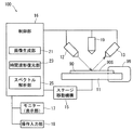
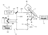
図1は、実施形態に係る検査装置100の概略構成図である。また、図2は、検査装置100が備える照射部12、検出部13および遅延部14の概略構成図である。
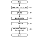
図7は、太陽電池90の検査例を示す流れ図である。なお、以下の説明においては、特に断らない限り、検査装置100の各動作が制御部16による制御下のもとに行われるものとする。また、各工程の内容に応じて、複数の工程が並列に実行されたり、複数の工程の実行順序が適宜変更されたりしてもよいものとする。
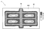
上記実施形態では、図2に示されるように、パルス光LP1が太陽電池90の表面90Sに対して斜めに照射され、検出器131が表面90S側に放射される電磁波LT1を検出している。しかしながら、例えば、太陽電池90の表面90Sに対して、パルス光LP11を垂直に照射し、これと同軸方向に反射するように放射される電磁波LT1を検出するように、検査装置100が構成されてもよい。なお、透明導電膜基板(ITO)を用いれば、パルス光LP11を透過させつつ、電磁波LT1を選択的に反射させて、その光路を変更することができる。
11 ステージ
12 照射部
121 フェムト秒レーザ
13 検出部
131 検出器
14 遅延部
15 ステージ移動機構
16 制御部
17 モニター
41,43 時間波形
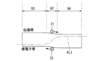
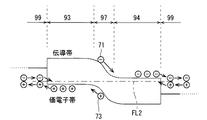
51 自由電子
53 正孔
61 スペクトル分布
71 自由電子
73 正孔
90,90A 太陽電池
90S,90SA 表面(受光面)
92,92A 裏面電極
93,93A,93B,93C p型半導体層
94,94A,94B,94C n型半導体層
96,96A 受光面電極
97 pn接合部
99 短絡手段
LP11 パルス光
LT1 電磁波
Claims (6)
- アノードおよびカソードを有する検査対象物を検査する検査装置であって、
前記検査対象物のアノードと、前記検査対象物のカソードを電気的に接続することによって短絡する短絡手段と、
前記短絡手段によって短絡された前記検査対象物に光を照射する照射部と、
前記照射部からの前記光の照射に応じて前記検査対象物から放射される電磁波を検出する検出部と、
を備えている、検査装置。 - 請求項1に記載の検査装置であって、
前記アノードがp型半導体であり、前記カソードがn型半導体である、検査装置。 - 請求項1または2に記載の検査装置であって、
前記検査対象物が、吸収波長領域が互いに相違する複数の太陽電池が積層されることによって構成される多接合型太陽電池である、検査装置。 - アノードおよびカソードを有する検査対象物を検査する検査方法であって、
(a) 前記アノードと前記カソードとを電気的に接続して短絡する工程と、
(b) 前記(a)工程にて短絡された状態の前記検査対象物に対して、光を照射し、当該光の照射に応じて、前記検査対象物から放射される電磁波を検出する工程と、
を含む、検査方法。 - 請求項4に記載の検査方法であって、
前記アノードがp型半導体であって、前記カソードがn型半導体である、検査方法。 - 請求項4または5に記載の検査方法であって、
前記検査対象物が、吸収波長領域が互いに相違する複数の太陽電池が積層されることによって構成される多接合型太陽電池である、検査方法。
Priority Applications (2)
| Application Number | Priority Date | Filing Date | Title |
|---|---|---|---|
| JP2013254807A JP6418542B2 (ja) | 2013-12-10 | 2013-12-10 | 検査装置および検査方法 |
| US14/566,428 US10158325B2 (en) | 2013-12-10 | 2014-12-10 | Inspection apparatus and inspection method |
Applications Claiming Priority (1)
| Application Number | Priority Date | Filing Date | Title |
|---|---|---|---|
| JP2013254807A JP6418542B2 (ja) | 2013-12-10 | 2013-12-10 | 検査装置および検査方法 |
Publications (2)
| Publication Number | Publication Date |
|---|---|
| JP2015114145A true JP2015114145A (ja) | 2015-06-22 |
| JP6418542B2 JP6418542B2 (ja) | 2018-11-07 |
Family
ID=53272197
Family Applications (1)
| Application Number | Title | Priority Date | Filing Date |
|---|---|---|---|
| JP2013254807A Expired - Fee Related JP6418542B2 (ja) | 2013-12-10 | 2013-12-10 | 検査装置および検査方法 |
Country Status (2)
| Country | Link |
|---|---|
| US (1) | US10158325B2 (ja) |
| JP (1) | JP6418542B2 (ja) |
Families Citing this family (10)
| Publication number | Priority date | Publication date | Assignee | Title |
|---|---|---|---|---|
| CN105229458A (zh) | 2013-03-14 | 2016-01-06 | 加州理工学院 | 检测电子和电化学能源单元异常 |
| WO2016103007A1 (fr) * | 2014-12-24 | 2016-06-30 | Arcelormittal | Procédé de contrôle d'un support comprenant un substrat métallique, un revêtement diélectrique, et une couche conductrice |
| MX388217B (es) | 2015-09-24 | 2025-03-19 | Hunt Perovskite Tech L L C | Sistema y método para probar la degradación del dispositivo fotosensible. |
| US10330732B2 (en) | 2015-10-01 | 2019-06-25 | California Institute Of Technology | Systems and methods for monitoring characteristics of energy units |
| JP6604629B2 (ja) * | 2016-02-15 | 2019-11-13 | 株式会社Screenホールディングス | 検査装置及び検査方法 |
| US10521897B2 (en) | 2016-07-22 | 2019-12-31 | International Business Machines Corporation | Using photonic emission to develop electromagnetic emission models |
| CN106849873B (zh) * | 2017-01-19 | 2018-11-02 | 深圳市量为科技有限公司 | 太阳能电池抗辐照能力无损检验方法及装置 |
| CN110133471B (zh) * | 2019-05-28 | 2021-02-12 | 中国工程物理研究院流体物理研究所 | 一种GaAs光导开关载流子浓度分布变化测试方法及光路 |
| KR20230164006A (ko) * | 2021-04-01 | 2023-12-01 | 하마마츠 포토닉스 가부시키가이샤 | 제조 방법, 검사 방법, 및 검사 장치 |
| EP4456418A1 (en) * | 2023-04-24 | 2024-10-30 | Valstybinis Moksliniu Tyrimu Institutas Fiziniu Ir Technologijos Mokslu Centras | Method and device for characterization of photovoltaic solar elements |
Citations (7)
| Publication number | Priority date | Publication date | Assignee | Title |
|---|---|---|---|---|
| JP2006024774A (ja) * | 2004-07-08 | 2006-01-26 | Institute Of Physical & Chemical Research | 半導体デバイスの故障診断方法と装置 |
| JP2010060317A (ja) * | 2008-09-01 | 2010-03-18 | Hamamatsu Photonics Kk | 半導体検査装置及び検査方法 |
| US20130037109A1 (en) * | 2010-03-09 | 2013-02-14 | The Regents Of The University Of Michigan | Methods of making organic photovoltaic cells having improved heterojunction morphology |
| JP2013061219A (ja) * | 2011-09-13 | 2013-04-04 | Dainippon Screen Mfg Co Ltd | 検査方法および検査装置 |
| JP2013072843A (ja) * | 2011-09-29 | 2013-04-22 | Dainippon Screen Mfg Co Ltd | 半導体検査方法および半導体検査装置 |
| JP2013084784A (ja) * | 2011-10-11 | 2013-05-09 | Nippon Telegr & Teleph Corp <Ntt> | タンデム太陽電池セルおよびその製造方法 |
| JP2013526082A (ja) * | 2010-05-05 | 2013-06-20 | ザ リージェンツ オブ ザ ユニヴァシティ オブ ミシガン | 有機ドナー‐アクセプタヘテロ接合における励起子解離の改善方法 |
Family Cites Families (17)
| Publication number | Priority date | Publication date | Assignee | Title |
|---|---|---|---|---|
| US3337782A (en) * | 1964-04-01 | 1967-08-22 | Westinghouse Electric Corp | Semiconductor controlled rectifier having a shorted emitter at a plurality of points |
| KR100472888B1 (ko) * | 1999-01-19 | 2005-03-08 | 캐논 가부시끼가이샤 | 화상 형성 장치의 제조 방법 |
| JP3657143B2 (ja) * | 1999-04-27 | 2005-06-08 | シャープ株式会社 | 太陽電池及びその製造方法 |
| DE10163463B9 (de) * | 2001-12-21 | 2008-07-17 | Osram Opto Semiconductors Gmbh | Vorrichtung und Verfahren zu in-situ-Messung von auf Trägern aufgedruckten Polymermengen |
| DE102005037573B4 (de) * | 2005-08-09 | 2007-05-31 | Infineon Technologies Ag | Thyristor mit Freiwerdeschutz in Form eines Thyristorsystems und Verfahren zur Herstellung des Thyristorsystems |
| JP4773839B2 (ja) * | 2006-02-15 | 2011-09-14 | キヤノン株式会社 | 対象物の情報を検出する検出装置 |
| US7518135B2 (en) * | 2006-12-20 | 2009-04-14 | Asml Netherlands B.V. | Reducing fast ions in a plasma radiation source |
| JP4975001B2 (ja) | 2007-12-28 | 2012-07-11 | キヤノン株式会社 | 波形情報取得装置及び波形情報取得方法 |
| CN101971040B (zh) * | 2008-02-22 | 2014-11-26 | 弗朗霍夫应用科学研究促进协会 | 用于表征半导体构件的测量方法和装置 |
| JP2011236104A (ja) * | 2010-05-13 | 2011-11-24 | Sony Corp | 酸化チタン構造体及びその製造方法、並びに酸化チタン構造体を用いた光電変換装置 |
| JP5804362B2 (ja) | 2011-07-14 | 2015-11-04 | 株式会社Screenホールディングス | 検査装置および検査方法 |
| EP2546634B1 (en) | 2011-07-14 | 2019-04-17 | SCREEN Holdings Co., Ltd. | Inspection apparatus and inspection method |
| JP6078870B2 (ja) * | 2012-06-28 | 2017-02-15 | 株式会社Screenホールディングス | 検査装置および検査方法 |
| JP6044893B2 (ja) * | 2013-03-08 | 2016-12-14 | 株式会社Screenホールディングス | 検査装置および検査方法 |
| JP6342622B2 (ja) * | 2013-07-10 | 2018-06-13 | 株式会社Screenホールディングス | フォトデバイス検査装置およびフォトデバイス検査方法 |
| JP6406656B2 (ja) * | 2013-08-23 | 2018-10-17 | 株式会社Screenホールディングス | 検査装置および検査方法 |
| JP6395206B2 (ja) * | 2014-03-25 | 2018-09-26 | 株式会社Screenホールディングス | 検査装置および検査方法 |
-
2013
- 2013-12-10 JP JP2013254807A patent/JP6418542B2/ja not_active Expired - Fee Related
-
2014
- 2014-12-10 US US14/566,428 patent/US10158325B2/en not_active Expired - Fee Related
Patent Citations (7)
| Publication number | Priority date | Publication date | Assignee | Title |
|---|---|---|---|---|
| JP2006024774A (ja) * | 2004-07-08 | 2006-01-26 | Institute Of Physical & Chemical Research | 半導体デバイスの故障診断方法と装置 |
| JP2010060317A (ja) * | 2008-09-01 | 2010-03-18 | Hamamatsu Photonics Kk | 半導体検査装置及び検査方法 |
| US20130037109A1 (en) * | 2010-03-09 | 2013-02-14 | The Regents Of The University Of Michigan | Methods of making organic photovoltaic cells having improved heterojunction morphology |
| JP2013526082A (ja) * | 2010-05-05 | 2013-06-20 | ザ リージェンツ オブ ザ ユニヴァシティ オブ ミシガン | 有機ドナー‐アクセプタヘテロ接合における励起子解離の改善方法 |
| JP2013061219A (ja) * | 2011-09-13 | 2013-04-04 | Dainippon Screen Mfg Co Ltd | 検査方法および検査装置 |
| JP2013072843A (ja) * | 2011-09-29 | 2013-04-22 | Dainippon Screen Mfg Co Ltd | 半導体検査方法および半導体検査装置 |
| JP2013084784A (ja) * | 2011-10-11 | 2013-05-09 | Nippon Telegr & Teleph Corp <Ntt> | タンデム太陽電池セルおよびその製造方法 |
Non-Patent Citations (1)
| Title |
|---|
| TARDON S , ET AL: "Photoluminescence studies of a-Si:H/c-Si-heterojunction solar cells", JOURNAL OF NON-CRYSTALLINE SOLIDS, vol. Vol.338-340, JPN6017027909, 15 June 2004 (2004-06-15), pages 444 - 447, ISSN: 0003735843 * |
Also Published As
| Publication number | Publication date |
|---|---|
| US20150162872A1 (en) | 2015-06-11 |
| JP6418542B2 (ja) | 2018-11-07 |
| US10158325B2 (en) | 2018-12-18 |
Similar Documents
| Publication | Publication Date | Title |
|---|---|---|
| JP6418542B2 (ja) | 検査装置および検査方法 | |
| US9450536B2 (en) | Inspection apparatus and inspection method | |
| JP5804362B2 (ja) | 検査装置および検査方法 | |
| JP5892597B2 (ja) | 検査装置および検査方法 | |
| JP6078870B2 (ja) | 検査装置および検査方法 | |
| US8872114B2 (en) | Inspection apparatus and inspection method | |
| US9541508B2 (en) | Inspecting device and inspecting method | |
| JP5822194B2 (ja) | 半導体検査方法および半導体検査装置 | |
| JP5835795B2 (ja) | 検査方法および検査装置 | |
| Nakanishi et al. | Comparison between laser terahertz emission microscope and conventional methods for analysis of polycrystalline silicon solar cell | |
| JP6342622B2 (ja) | フォトデバイス検査装置およびフォトデバイス検査方法 | |
| JP2015184170A (ja) | 検査装置および検査方法 | |
| JP2014192444A (ja) | 検査装置および検査方法 | |
| JP6078869B2 (ja) | 検査装置および検査方法 | |
| JP5929293B2 (ja) | 検査装置および検査方法 | |
| JP2021048351A (ja) | 検査方法および検査装置 | |
| JP2016029345A (ja) | 検査装置および検査方法 | |
| JP6958833B2 (ja) | 半導体検査装置及び半導体検査方法 | |
| JP2019058042A (ja) | 検査装置および検査方法 | |
| JP6355100B2 (ja) | 検査装置および検査方法 | |
| JP6161059B2 (ja) | フォトデバイス検査装置およびフォトデバイス検査方法 | |
| JP2017157692A (ja) | 検査装置及び検査方法 | |
| JP2016151536A (ja) | 検査装置および検査方法 | |
| Nakanishi et al. | Imaging of local photo-excited current in solar cell using a laser terahertz emission microscope | |
| JP2014102233A (ja) | 電磁波計測装置および電磁波計測方法 |
Legal Events
| Date | Code | Title | Description |
|---|---|---|---|
| A621 | Written request for application examination |
Free format text: JAPANESE INTERMEDIATE CODE: A621 Effective date: 20160721 |
|
| A521 | Request for written amendment filed |
Free format text: JAPANESE INTERMEDIATE CODE: A821 Effective date: 20160721 |
|
| A131 | Notification of reasons for refusal |
Free format text: JAPANESE INTERMEDIATE CODE: A131 Effective date: 20170801 |
|
| A521 | Request for written amendment filed |
Free format text: JAPANESE INTERMEDIATE CODE: A523 Effective date: 20171002 |
|
| A131 | Notification of reasons for refusal |
Free format text: JAPANESE INTERMEDIATE CODE: A131 Effective date: 20180213 |
|
| A521 | Request for written amendment filed |
Free format text: JAPANESE INTERMEDIATE CODE: A523 Effective date: 20180416 |
|
| TRDD | Decision of grant or rejection written | ||
| A01 | Written decision to grant a patent or to grant a registration (utility model) |
Free format text: JAPANESE INTERMEDIATE CODE: A01 Effective date: 20180918 |
|
| A61 | First payment of annual fees (during grant procedure) |
Free format text: JAPANESE INTERMEDIATE CODE: A61 Effective date: 20181001 |
|
| R150 | Certificate of patent or registration of utility model |
Ref document number: 6418542 Country of ref document: JP Free format text: JAPANESE INTERMEDIATE CODE: R150 |
|
| R250 | Receipt of annual fees |
Free format text: JAPANESE INTERMEDIATE CODE: R250 |
|
| R250 | Receipt of annual fees |
Free format text: JAPANESE INTERMEDIATE CODE: R250 |
|
| LAPS | Cancellation because of no payment of annual fees |