JP2014092772A - 液晶表示装置 - Google Patents
液晶表示装置 Download PDFInfo
- Publication number
- JP2014092772A JP2014092772A JP2012245185A JP2012245185A JP2014092772A JP 2014092772 A JP2014092772 A JP 2014092772A JP 2012245185 A JP2012245185 A JP 2012245185A JP 2012245185 A JP2012245185 A JP 2012245185A JP 2014092772 A JP2014092772 A JP 2014092772A
- Authority
- JP
- Japan
- Prior art keywords
- light shielding
- liquid crystal
- crystal display
- light
- disposed
- Prior art date
- Legal status (The legal status is an assumption and is not a legal conclusion. Google has not performed a legal analysis and makes no representation as to the accuracy of the status listed.)
- Pending
Links
Images


Classifications
-
- G—PHYSICS
- G02—OPTICS
- G02F—OPTICAL DEVICES OR ARRANGEMENTS FOR THE CONTROL OF LIGHT BY MODIFICATION OF THE OPTICAL PROPERTIES OF THE MEDIA OF THE ELEMENTS INVOLVED THEREIN; NON-LINEAR OPTICS; FREQUENCY-CHANGING OF LIGHT; OPTICAL LOGIC ELEMENTS; OPTICAL ANALOGUE/DIGITAL CONVERTERS
- G02F1/00—Devices or arrangements for the control of the intensity, colour, phase, polarisation or direction of light arriving from an independent light source, e.g. switching, gating or modulating; Non-linear optics
- G02F1/01—Devices or arrangements for the control of the intensity, colour, phase, polarisation or direction of light arriving from an independent light source, e.g. switching, gating or modulating; Non-linear optics for the control of the intensity, phase, polarisation or colour
- G02F1/13—Devices or arrangements for the control of the intensity, colour, phase, polarisation or direction of light arriving from an independent light source, e.g. switching, gating or modulating; Non-linear optics for the control of the intensity, phase, polarisation or colour based on liquid crystals, e.g. single liquid crystal display cells
- G02F1/133—Constructional arrangements; Operation of liquid crystal cells; Circuit arrangements
- G02F1/1333—Constructional arrangements; Manufacturing methods
- G02F1/1335—Structural association of cells with optical devices, e.g. polarisers or reflectors
- G02F1/133509—Filters, e.g. light shielding masks
- G02F1/133512—Light shielding layers, e.g. black matrix
-
- G—PHYSICS
- G02—OPTICS
- G02F—OPTICAL DEVICES OR ARRANGEMENTS FOR THE CONTROL OF LIGHT BY MODIFICATION OF THE OPTICAL PROPERTIES OF THE MEDIA OF THE ELEMENTS INVOLVED THEREIN; NON-LINEAR OPTICS; FREQUENCY-CHANGING OF LIGHT; OPTICAL LOGIC ELEMENTS; OPTICAL ANALOGUE/DIGITAL CONVERTERS
- G02F1/00—Devices or arrangements for the control of the intensity, colour, phase, polarisation or direction of light arriving from an independent light source, e.g. switching, gating or modulating; Non-linear optics
- G02F1/01—Devices or arrangements for the control of the intensity, colour, phase, polarisation or direction of light arriving from an independent light source, e.g. switching, gating or modulating; Non-linear optics for the control of the intensity, phase, polarisation or colour
- G02F1/13—Devices or arrangements for the control of the intensity, colour, phase, polarisation or direction of light arriving from an independent light source, e.g. switching, gating or modulating; Non-linear optics for the control of the intensity, phase, polarisation or colour based on liquid crystals, e.g. single liquid crystal display cells
- G02F1/133—Constructional arrangements; Operation of liquid crystal cells; Circuit arrangements
- G02F1/1333—Constructional arrangements; Manufacturing methods
- G02F1/133351—Manufacturing of individual cells out of a plurality of cells, e.g. by dicing
-
- G—PHYSICS
- G02—OPTICS
- G02F—OPTICAL DEVICES OR ARRANGEMENTS FOR THE CONTROL OF LIGHT BY MODIFICATION OF THE OPTICAL PROPERTIES OF THE MEDIA OF THE ELEMENTS INVOLVED THEREIN; NON-LINEAR OPTICS; FREQUENCY-CHANGING OF LIGHT; OPTICAL LOGIC ELEMENTS; OPTICAL ANALOGUE/DIGITAL CONVERTERS
- G02F1/00—Devices or arrangements for the control of the intensity, colour, phase, polarisation or direction of light arriving from an independent light source, e.g. switching, gating or modulating; Non-linear optics
- G02F1/01—Devices or arrangements for the control of the intensity, colour, phase, polarisation or direction of light arriving from an independent light source, e.g. switching, gating or modulating; Non-linear optics for the control of the intensity, phase, polarisation or colour
- G02F1/13—Devices or arrangements for the control of the intensity, colour, phase, polarisation or direction of light arriving from an independent light source, e.g. switching, gating or modulating; Non-linear optics for the control of the intensity, phase, polarisation or colour based on liquid crystals, e.g. single liquid crystal display cells
- G02F1/133—Constructional arrangements; Operation of liquid crystal cells; Circuit arrangements
- G02F1/1333—Constructional arrangements; Manufacturing methods
- G02F1/133388—Constructional arrangements; Manufacturing methods with constructional differences between the display region and the peripheral region
Landscapes
- Physics & Mathematics (AREA)
- Nonlinear Science (AREA)
- Mathematical Physics (AREA)
- Chemical & Material Sciences (AREA)
- Crystallography & Structural Chemistry (AREA)
- General Physics & Mathematics (AREA)
- Optics & Photonics (AREA)
- Engineering & Computer Science (AREA)
- Manufacturing & Machinery (AREA)
- Devices For Indicating Variable Information By Combining Individual Elements (AREA)
- Liquid Crystal (AREA)
Priority Applications (5)
| Application Number | Priority Date | Filing Date | Title |
|---|---|---|---|
| JP2012245185A JP2014092772A (ja) | 2012-11-07 | 2012-11-07 | 液晶表示装置 |
| TW102138547A TWI515482B (zh) | 2012-11-07 | 2013-10-24 | 液晶顯示裝置 |
| US14/065,610 US9146416B2 (en) | 2012-11-07 | 2013-10-29 | Liquid crystal display apparatus |
| KR1020130132747A KR20140059131A (ko) | 2012-11-07 | 2013-11-04 | 액정 표시 장치 |
| CN201310547951.6A CN103809322A (zh) | 2012-11-07 | 2013-11-07 | 液晶显示装置 |
Applications Claiming Priority (1)
| Application Number | Priority Date | Filing Date | Title |
|---|---|---|---|
| JP2012245185A JP2014092772A (ja) | 2012-11-07 | 2012-11-07 | 液晶表示装置 |
Publications (2)
| Publication Number | Publication Date |
|---|---|
| JP2014092772A true JP2014092772A (ja) | 2014-05-19 |
| JP2014092772A5 JP2014092772A5 (enExample) | 2015-12-24 |
Family
ID=50622051
Family Applications (1)
| Application Number | Title | Priority Date | Filing Date |
|---|---|---|---|
| JP2012245185A Pending JP2014092772A (ja) | 2012-11-07 | 2012-11-07 | 液晶表示装置 |
Country Status (5)
| Country | Link |
|---|---|
| US (1) | US9146416B2 (enExample) |
| JP (1) | JP2014092772A (enExample) |
| KR (1) | KR20140059131A (enExample) |
| CN (1) | CN103809322A (enExample) |
| TW (1) | TWI515482B (enExample) |
Families Citing this family (5)
| Publication number | Priority date | Publication date | Assignee | Title |
|---|---|---|---|---|
| CN103792736B (zh) * | 2014-01-24 | 2016-08-31 | 北京京东方显示技术有限公司 | 一种对盒后的母板、液晶显示面板及对应的制作方法 |
| JP2015195106A (ja) | 2014-03-31 | 2015-11-05 | 株式会社ジャパンディスプレイ | 有機el表示装置及びその製造方法 |
| TWI557831B (zh) * | 2015-05-15 | 2016-11-11 | 友達光電股份有限公司 | 微組件的傳送方法 |
| EP3449532B1 (en) | 2016-04-28 | 2024-02-28 | AT & S Austria Technologie & Systemtechnik Aktiengesellschaft | Component carrier with integrated antenna arrangement, electronic apparatus, radio communication method |
| TWI685779B (zh) * | 2019-01-30 | 2020-02-21 | 友達光電股份有限公司 | 觸控裝置 |
Citations (5)
| Publication number | Priority date | Publication date | Assignee | Title |
|---|---|---|---|---|
| JP2003043462A (ja) * | 2001-07-30 | 2003-02-13 | Nec Corp | 液晶表示装置及びその製造方法 |
| US20050062910A1 (en) * | 2003-09-24 | 2005-03-24 | Hung-Jen Chu | [liquid crystal display device and fabricating method thereof] |
| JP2006053169A (ja) * | 2004-07-15 | 2006-02-23 | Optrex Corp | 液晶表示素子 |
| JP2006084713A (ja) * | 2004-09-15 | 2006-03-30 | Sharp Corp | 液晶表示装置 |
| WO2006098475A1 (ja) * | 2005-03-18 | 2006-09-21 | Sharp Kabushiki Kaisha | パネルおよびその製造方法 |
Family Cites Families (12)
| Publication number | Priority date | Publication date | Assignee | Title |
|---|---|---|---|---|
| JP4851651B2 (ja) | 2001-01-31 | 2012-01-11 | オプトレックス株式会社 | 液晶表示素子 |
| TWI259308B (en) * | 2001-04-17 | 2006-08-01 | Nec Lcd Technologies Ltd | Liquid-crystal display device and method of fabricating same |
| JP4156216B2 (ja) | 2001-06-19 | 2008-09-24 | 株式会社 日立ディスプレイズ | 液晶表示装置 |
| CN1185531C (zh) * | 2001-10-09 | 2005-01-19 | 瀚宇彩晶股份有限公司 | 薄膜晶体管液晶显示装置及制造方法 |
| JP2004077703A (ja) | 2002-08-14 | 2004-03-11 | Toshiba Corp | 液晶表示装置 |
| JP4133171B2 (ja) | 2002-09-27 | 2008-08-13 | オプトレックス株式会社 | 半透過反射型液晶表示パネル |
| US7432994B2 (en) * | 2003-11-20 | 2008-10-07 | Chunghwa Picture Tubes, Ltd. | Liquid crystal display device and fabrication method thereof |
| US7385660B2 (en) * | 2003-12-08 | 2008-06-10 | Sharp Kabushiki Kaisha | Liquid crystal display device for transflector having opening in a first electrode for forming a liquid crystal domain and openings at first and second corners of the domain on a second electrode |
| US7965365B2 (en) | 2004-09-03 | 2011-06-21 | Nec Lcd Technologies, Ltd | Image display device, portable terminal, display panel, and lens |
| TWI287153B (en) | 2005-08-08 | 2007-09-21 | Au Optronics Corp | Backlight module structure |
| KR101450803B1 (ko) | 2007-12-28 | 2014-10-15 | 삼성디스플레이 주식회사 | 어레이 기판 및 어레이 기판의 제조방법 |
| TWI409778B (zh) | 2008-12-25 | 2013-09-21 | Innolux Corp | 液晶顯示裝置、液晶顯示面板及驅動方法 |
-
2012
- 2012-11-07 JP JP2012245185A patent/JP2014092772A/ja active Pending
-
2013
- 2013-10-24 TW TW102138547A patent/TWI515482B/zh active
- 2013-10-29 US US14/065,610 patent/US9146416B2/en active Active
- 2013-11-04 KR KR1020130132747A patent/KR20140059131A/ko not_active Ceased
- 2013-11-07 CN CN201310547951.6A patent/CN103809322A/zh active Pending
Patent Citations (5)
| Publication number | Priority date | Publication date | Assignee | Title |
|---|---|---|---|---|
| JP2003043462A (ja) * | 2001-07-30 | 2003-02-13 | Nec Corp | 液晶表示装置及びその製造方法 |
| US20050062910A1 (en) * | 2003-09-24 | 2005-03-24 | Hung-Jen Chu | [liquid crystal display device and fabricating method thereof] |
| JP2006053169A (ja) * | 2004-07-15 | 2006-02-23 | Optrex Corp | 液晶表示素子 |
| JP2006084713A (ja) * | 2004-09-15 | 2006-03-30 | Sharp Corp | 液晶表示装置 |
| WO2006098475A1 (ja) * | 2005-03-18 | 2006-09-21 | Sharp Kabushiki Kaisha | パネルおよびその製造方法 |
Also Published As
| Publication number | Publication date |
|---|---|
| CN103809322A (zh) | 2014-05-21 |
| US9146416B2 (en) | 2015-09-29 |
| TWI515482B (zh) | 2016-01-01 |
| TW201423221A (zh) | 2014-06-16 |
| KR20140059131A (ko) | 2014-05-15 |
| US20140125927A1 (en) | 2014-05-08 |
Similar Documents
| Publication | Publication Date | Title |
|---|---|---|
| JP6055089B2 (ja) | 表示装置 | |
| KR101439046B1 (ko) | 액정 표시 장치 | |
| JP5752030B2 (ja) | 液晶表示装置 | |
| US11199934B2 (en) | Display device with position input function | |
| CN105739204B (zh) | 液晶显示装置 | |
| KR20160083339A (ko) | 터치 방식 액정표시장치 | |
| JP2017067874A (ja) | 表示装置およびその製造方法 | |
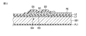
| JP2014092772A (ja) | 液晶表示装置 | |
| US20180314098A1 (en) | Display board and display device | |
| JP5410024B2 (ja) | アレイ基板及びこれを有する表示パネル | |
| JP2008225473A5 (enExample) | ||
| KR20140097774A (ko) | 액정표시장치 | |
| KR101904979B1 (ko) | 네로우 베젤 타입 액정표시장치 | |
| KR101951224B1 (ko) | 액정표시장치 | |
| WO2018225603A1 (ja) | 位置入力機能付き表示装置 | |
| JP2009258346A (ja) | 電気光学装置及び投射型表示装置 | |
| KR20140087621A (ko) | 유기발광표시장치 및 그의 제조방법 | |
| JP2007024963A (ja) | 液晶表示装置 | |
| CN109946893A (zh) | 显示装置 | |
| JP5218262B2 (ja) | 表示パネルとそれを用いる表示モジュール | |
| KR102207621B1 (ko) | 액정표시장치 | |
| WO2019021924A1 (ja) | 表示パネル | |
| KR102427765B1 (ko) | 표시패널 및 표시장치 | |
| KR20150111545A (ko) | 표시 장치 | |
| WO2022158477A1 (ja) | 表示装置 |
Legal Events
| Date | Code | Title | Description |
|---|---|---|---|
| A521 | Request for written amendment filed |
Free format text: JAPANESE INTERMEDIATE CODE: A523 Effective date: 20151106 |
|
| A621 | Written request for application examination |
Free format text: JAPANESE INTERMEDIATE CODE: A621 Effective date: 20151106 |
|
| A977 | Report on retrieval |
Free format text: JAPANESE INTERMEDIATE CODE: A971007 Effective date: 20160713 |
|
| A131 | Notification of reasons for refusal |
Free format text: JAPANESE INTERMEDIATE CODE: A131 Effective date: 20160719 |
|
| A02 | Decision of refusal |
Free format text: JAPANESE INTERMEDIATE CODE: A02 Effective date: 20170131 |