JP2013532907A - 太陽光発電装置及びその製造方法 - Google Patents
太陽光発電装置及びその製造方法 Download PDFInfo
- Publication number
- JP2013532907A JP2013532907A JP2013521675A JP2013521675A JP2013532907A JP 2013532907 A JP2013532907 A JP 2013532907A JP 2013521675 A JP2013521675 A JP 2013521675A JP 2013521675 A JP2013521675 A JP 2013521675A JP 2013532907 A JP2013532907 A JP 2013532907A
- Authority
- JP
- Japan
- Prior art keywords
- cell
- connection member
- power generation
- via hole
- insulating film
- Prior art date
- Legal status (The legal status is an assumption and is not a legal conclusion. Google has not performed a legal analysis and makes no representation as to the accuracy of the status listed.)
- Pending
Links
- 238000010248 power generation Methods 0.000 title claims abstract description 40
- 238000004519 manufacturing process Methods 0.000 title claims abstract description 18
- 239000000758 substrate Substances 0.000 claims abstract description 36
- 238000000034 method Methods 0.000 claims abstract description 33
- 238000007747 plating Methods 0.000 claims description 27
- 230000031700 light absorption Effects 0.000 claims description 20
- 239000006096 absorbing agent Substances 0.000 claims description 7
- 238000009713 electroplating Methods 0.000 claims description 5
- 239000000872 buffer Substances 0.000 description 40
- 239000010949 copper Substances 0.000 description 11
- XLOMVQKBTHCTTD-UHFFFAOYSA-N Zinc monoxide Chemical compound [Zn]=O XLOMVQKBTHCTTD-UHFFFAOYSA-N 0.000 description 10
- RYGMFSIKBFXOCR-UHFFFAOYSA-N Copper Chemical compound [Cu] RYGMFSIKBFXOCR-UHFFFAOYSA-N 0.000 description 8
- 229910052802 copper Inorganic materials 0.000 description 8
- 229910052733 gallium Inorganic materials 0.000 description 8
- 238000004544 sputter deposition Methods 0.000 description 8
- 229910052738 indium Inorganic materials 0.000 description 7
- 239000000463 material Substances 0.000 description 6
- 229910052751 metal Inorganic materials 0.000 description 6
- 239000002184 metal Substances 0.000 description 6
- GYHNNYVSQQEPJS-UHFFFAOYSA-N Gallium Chemical compound [Ga] GYHNNYVSQQEPJS-UHFFFAOYSA-N 0.000 description 5
- 238000007639 printing Methods 0.000 description 5
- 239000011787 zinc oxide Substances 0.000 description 5
- KTSFMFGEAAANTF-UHFFFAOYSA-N [Cu].[Se].[Se].[In] Chemical compound [Cu].[Se].[Se].[In] KTSFMFGEAAANTF-UHFFFAOYSA-N 0.000 description 4
- APFVFJFRJDLVQX-UHFFFAOYSA-N indium atom Chemical compound [In] APFVFJFRJDLVQX-UHFFFAOYSA-N 0.000 description 4
- 239000002243 precursor Substances 0.000 description 4
- 239000011669 selenium Substances 0.000 description 4
- WUPHOULIZUERAE-UHFFFAOYSA-N 3-(oxolan-2-yl)propanoic acid Chemical compound OC(=O)CCC1CCCO1 WUPHOULIZUERAE-UHFFFAOYSA-N 0.000 description 3
- 239000004642 Polyimide Substances 0.000 description 3
- BQCADISMDOOEFD-UHFFFAOYSA-N Silver Chemical compound [Ag] BQCADISMDOOEFD-UHFFFAOYSA-N 0.000 description 3
- 229910052980 cadmium sulfide Inorganic materials 0.000 description 3
- 239000004020 conductor Substances 0.000 description 3
- 239000005038 ethylene vinyl acetate Substances 0.000 description 3
- 239000012212 insulator Substances 0.000 description 3
- 238000012986 modification Methods 0.000 description 3
- 230000004048 modification Effects 0.000 description 3
- 229920001721 polyimide Polymers 0.000 description 3
- 229910052709 silver Inorganic materials 0.000 description 3
- 239000004332 silver Substances 0.000 description 3
- CIWBSHSKHKDKBQ-JLAZNSOCSA-N Ascorbic acid Chemical compound OC[C@H](O)[C@H]1OC(=O)C(O)=C1O CIWBSHSKHKDKBQ-JLAZNSOCSA-N 0.000 description 2
- ZOKXTWBITQBERF-UHFFFAOYSA-N Molybdenum Chemical compound [Mo] ZOKXTWBITQBERF-UHFFFAOYSA-N 0.000 description 2
- 229910052782 aluminium Inorganic materials 0.000 description 2
- XAGFODPZIPBFFR-UHFFFAOYSA-N aluminium Chemical compound [Al] XAGFODPZIPBFFR-UHFFFAOYSA-N 0.000 description 2
- DQXBYHZEEUGOBF-UHFFFAOYSA-N but-3-enoic acid;ethene Chemical compound C=C.OC(=O)CC=C DQXBYHZEEUGOBF-UHFFFAOYSA-N 0.000 description 2
- 150000001875 compounds Chemical class 0.000 description 2
- 239000013078 crystal Substances 0.000 description 2
- 238000000151 deposition Methods 0.000 description 2
- 230000000694 effects Effects 0.000 description 2
- 239000003792 electrolyte Substances 0.000 description 2
- 238000001704 evaporation Methods 0.000 description 2
- 229910021645 metal ion Inorganic materials 0.000 description 2
- 229910052750 molybdenum Inorganic materials 0.000 description 2
- 239000011733 molybdenum Substances 0.000 description 2
- 229920001200 poly(ethylene-vinyl acetate) Polymers 0.000 description 2
- 238000003860 storage Methods 0.000 description 2
- JPVYNHNXODAKFH-UHFFFAOYSA-N Cu2+ Chemical compound [Cu+2] JPVYNHNXODAKFH-UHFFFAOYSA-N 0.000 description 1
- BUGBHKTXTAQXES-UHFFFAOYSA-N Selenium Chemical compound [Se] BUGBHKTXTAQXES-UHFFFAOYSA-N 0.000 description 1
- XUIMIQQOPSSXEZ-UHFFFAOYSA-N Silicon Chemical compound [Si] XUIMIQQOPSSXEZ-UHFFFAOYSA-N 0.000 description 1
- 229910001431 copper ion Inorganic materials 0.000 description 1
- YNLHHZNOLUDEKQ-UHFFFAOYSA-N copper;selanylidenegallium Chemical compound [Cu].[Se]=[Ga] YNLHHZNOLUDEKQ-UHFFFAOYSA-N 0.000 description 1
- 238000001035 drying Methods 0.000 description 1
- 239000011521 glass Substances 0.000 description 1
- PCHJSUWPFVWCPO-UHFFFAOYSA-N gold Chemical compound [Au] PCHJSUWPFVWCPO-UHFFFAOYSA-N 0.000 description 1
- 229910052737 gold Inorganic materials 0.000 description 1
- 239000010931 gold Substances 0.000 description 1
- 238000010438 heat treatment Methods 0.000 description 1
- 239000012535 impurity Substances 0.000 description 1
- 239000011159 matrix material Substances 0.000 description 1
- 239000002923 metal particle Substances 0.000 description 1
- 239000002245 particle Substances 0.000 description 1
- -1 polyethylene terephthalate Polymers 0.000 description 1
- 229920000139 polyethylene terephthalate Polymers 0.000 description 1
- 239000005020 polyethylene terephthalate Substances 0.000 description 1
- 229920000307 polymer substrate Polymers 0.000 description 1
- 238000007650 screen-printing Methods 0.000 description 1
- 229910052711 selenium Inorganic materials 0.000 description 1
- 239000004065 semiconductor Substances 0.000 description 1
- 229910052710 silicon Inorganic materials 0.000 description 1
- 239000010703 silicon Substances 0.000 description 1
- 229910001220 stainless steel Inorganic materials 0.000 description 1
- 239000010935 stainless steel Substances 0.000 description 1
- 239000000126 substance Substances 0.000 description 1
- 238000002834 transmittance Methods 0.000 description 1
- 238000001771 vacuum deposition Methods 0.000 description 1
Images


Classifications
-
- H—ELECTRICITY
- H01—ELECTRIC ELEMENTS
- H01L—SEMICONDUCTOR DEVICES NOT COVERED BY CLASS H10
- H01L31/00—Semiconductor devices sensitive to infrared radiation, light, electromagnetic radiation of shorter wavelength or corpuscular radiation and specially adapted either for the conversion of the energy of such radiation into electrical energy or for the control of electrical energy by such radiation; Processes or apparatus specially adapted for the manufacture or treatment thereof or of parts thereof; Details thereof
- H01L31/02—Details
- H01L31/02016—Circuit arrangements of general character for the devices
- H01L31/02019—Circuit arrangements of general character for the devices for devices characterised by at least one potential jump barrier or surface barrier
- H01L31/02021—Circuit arrangements of general character for the devices for devices characterised by at least one potential jump barrier or surface barrier for solar cells
-
- H—ELECTRICITY
- H01—ELECTRIC ELEMENTS
- H01L—SEMICONDUCTOR DEVICES NOT COVERED BY CLASS H10
- H01L31/00—Semiconductor devices sensitive to infrared radiation, light, electromagnetic radiation of shorter wavelength or corpuscular radiation and specially adapted either for the conversion of the energy of such radiation into electrical energy or for the control of electrical energy by such radiation; Processes or apparatus specially adapted for the manufacture or treatment thereof or of parts thereof; Details thereof
- H01L31/02—Details
- H01L31/0224—Electrodes
- H01L31/022408—Electrodes for devices characterised by at least one potential jump barrier or surface barrier
- H01L31/022425—Electrodes for devices characterised by at least one potential jump barrier or surface barrier for solar cells
-
- H—ELECTRICITY
- H01—ELECTRIC ELEMENTS
- H01L—SEMICONDUCTOR DEVICES NOT COVERED BY CLASS H10
- H01L31/00—Semiconductor devices sensitive to infrared radiation, light, electromagnetic radiation of shorter wavelength or corpuscular radiation and specially adapted either for the conversion of the energy of such radiation into electrical energy or for the control of electrical energy by such radiation; Processes or apparatus specially adapted for the manufacture or treatment thereof or of parts thereof; Details thereof
- H01L31/04—Semiconductor devices sensitive to infrared radiation, light, electromagnetic radiation of shorter wavelength or corpuscular radiation and specially adapted either for the conversion of the energy of such radiation into electrical energy or for the control of electrical energy by such radiation; Processes or apparatus specially adapted for the manufacture or treatment thereof or of parts thereof; Details thereof adapted as photovoltaic [PV] conversion devices
- H01L31/042—PV modules or arrays of single PV cells
- H01L31/0445—PV modules or arrays of single PV cells including thin film solar cells, e.g. single thin film a-Si, CIS or CdTe solar cells
- H01L31/046—PV modules composed of a plurality of thin film solar cells deposited on the same substrate
- H01L31/0465—PV modules composed of a plurality of thin film solar cells deposited on the same substrate comprising particular structures for the electrical interconnection of adjacent PV cells in the module
-
- Y—GENERAL TAGGING OF NEW TECHNOLOGICAL DEVELOPMENTS; GENERAL TAGGING OF CROSS-SECTIONAL TECHNOLOGIES SPANNING OVER SEVERAL SECTIONS OF THE IPC; TECHNICAL SUBJECTS COVERED BY FORMER USPC CROSS-REFERENCE ART COLLECTIONS [XRACs] AND DIGESTS
- Y02—TECHNOLOGIES OR APPLICATIONS FOR MITIGATION OR ADAPTATION AGAINST CLIMATE CHANGE
- Y02E—REDUCTION OF GREENHOUSE GAS [GHG] EMISSIONS, RELATED TO ENERGY GENERATION, TRANSMISSION OR DISTRIBUTION
- Y02E10/00—Energy generation through renewable energy sources
- Y02E10/50—Photovoltaic [PV] energy
Abstract
【選択図】図1
Description
Claims (17)
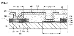
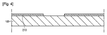
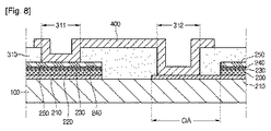
- 基板と、
前記基板の上に配置される第1セルと、
前記第1セルに隣接する第2セルと、
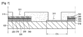
前記第1セル及び前記第2セルを覆う第1絶縁フィルムと、
前記第1セル及び前記第2セルを連結する接続部材と、を含み、
前記第1絶縁フィルムは、前記第1セルを露出する第1ビアホール及び前記第2セルを露出する第2ビアホールを含み、
前記接続部材は、前記第1ビアホール及び前記第2ビアホールを通じて、前記第1セル及び前記第2セルを連結することを特徴とする、太陽光発電装置。 - 前記第1絶縁フィルムの上に配置され、前記接続部材を覆う第2絶縁フィルムを含むことを特徴とする、請求項1に記載の太陽光発電装置。
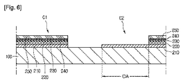
- 前記第1セルは、
前記基板の上に配置される第1後面電極と、
前記第1後面電極の上に配置される第1光吸収部と、
前記第1光吸収部の上に配置される第1ウィンドウと、を含み、
前記第2セルは、
前記基板の上に配置される第2後面電極と、
前記第2後面電極の上に配置される第2光吸収部と、
前記第2光吸収部の上に配置される第2ウィンドウと、を含み、
前記接続部材は、前記第1ウィンドウ及び前記第2後面電極を連結することを特徴とする請求項1に記載の太陽光発電装置。 - 前記接続部材は、前記第1ウィンドウの上面に直接接触し、前記第2後面電極の上面に直接接触することを特徴とする請求項3に記載の太陽光発電装置。
- 前記第2光吸収部は、前記第2後面電極層の上面が露出するように階段形状に積層されることを特徴とする請求項4に記載の太陽光発電装置。
- 前記接続部材及び前記第1セルの間及び前記接続部材及び前記第2セルの間に形成されるメッキ層を含むことを特徴とする請求項1に記載の太陽光発電装置。
- 前記基板及び前記接続部材はフレキシブルであることを特徴とする請求項1に記載の太陽光発電装置。
- 基板と、
前記基板の上に配置される第1セルと、
前記第1セルに隣接する第2セルと、
前記第1セル及び前記第2セルに連結される接続部材と、
前記接続部材の外部面にコーティングされるメッキ層と、
を含むことを特徴とする太陽光発電装置。 - 前記メッキ層は、前記第1セル及び前記接続部材の間に介されることを特徴とする請求項8に記載の太陽光発電装置。
- 前記メッキ層は、前記第2セル及び前記接続部材の間に介されることを特徴とする請求項9に記載の太陽光発電装置。
- 前記第1セル及び前記第2セルを覆う第1絶縁フィルムを含み、
前記第1絶縁フィルムは、前記第1セルを露出する第1ビアホール、及び前記第2セルを露出する第2ビアホールを含み、
前記接続部材は、前記第1ビアホール及び前記第2ビアホールを通じて、前記第1セル及び前記第2セルを連結することを特徴とする請求項9に記載の太陽光発電装置。 - 前記接続部材は、前記第1ビアホールの内、前記第2ビアホールの内、及び前記第1絶縁フィルムの上に亘って配置されることを特徴とする請求項11に記載の太陽光発電装置。
- 前記接続部材及び前記第1絶縁フィルムを覆う第2絶縁フィルムを含むことを特徴とする請求項12に記載の太陽光発電装置。
- 基板の上に隣り合う第1セル及び第2セルを形成するステップと、
前記第1セル及び前記第2セルを各々露出する第1ビアホール及び第2ビアホールが形成される第1絶縁フィルムを形成するステップと、
前記第1ビアホール及び前記第2ビアホールを通じて前記第1セル及び前記第2セルに接続される接続部材を形成するステップと、
を含むことを特徴とする太陽光発電装置の製造方法。 - 前記接続部材の外部面に、電気メッキによりメッキ層を形成するステップを含むことを特徴とする請求項14に記載の太陽光発電装置の製造方法。
- 前記メッキ層は、前記接続部材及び前記第1セルの間に形成されることを特徴とする請求項15に記載の太陽光発電装置の製造方法。
- 前記メッキ層は、前記接続部材及び前記第2セルの間に形成されることを特徴とする請求項16に記載の太陽光発電装置の製造方法。
Applications Claiming Priority (3)
| Application Number | Priority Date | Filing Date | Title |
|---|---|---|---|
| KR10-2010-0074417 | 2010-07-30 | ||
| KR1020100074417A KR101114099B1 (ko) | 2010-07-30 | 2010-07-30 | 태양광 발전장치 및 이의 제조방법 |
| PCT/KR2011/003124 WO2012015150A1 (ko) | 2010-07-30 | 2011-04-27 | 태양광 발전장치 및 이의 제조방법 |
Publications (2)
| Publication Number | Publication Date |
|---|---|
| JP2013532907A true JP2013532907A (ja) | 2013-08-19 |
| JP2013532907A5 JP2013532907A5 (ja) | 2014-07-17 |
Family
ID=45530315
Family Applications (1)
| Application Number | Title | Priority Date | Filing Date |
|---|---|---|---|
| JP2013521675A Pending JP2013532907A (ja) | 2010-07-30 | 2011-04-27 | 太陽光発電装置及びその製造方法 |
Country Status (6)
| Country | Link |
|---|---|
| US (1) | US9391215B2 (ja) |
| EP (1) | EP2511961A4 (ja) |
| JP (1) | JP2013532907A (ja) |
| KR (1) | KR101114099B1 (ja) |
| CN (1) | CN103201854A (ja) |
| WO (1) | WO2012015150A1 (ja) |
Families Citing this family (5)
| Publication number | Priority date | Publication date | Assignee | Title |
|---|---|---|---|---|
| ES2705199T3 (es) * | 2013-01-17 | 2019-03-22 | Atotech Deutschland Gmbh | Contactos eléctricos galvanizados para módulos solares |
| US9640331B2 (en) * | 2013-03-22 | 2017-05-02 | Sharp Laboratories Of America, Inc. | Solid state dye-sensitized solar cell tandem module |
| US20150037915A1 (en) * | 2013-07-31 | 2015-02-05 | Wei-Sheng Lei | Method and system for laser focus plane determination in a laser scribing process |
| DE112020001695T5 (de) * | 2019-03-29 | 2021-12-16 | Sunpower Corporation | Solarzellen mit Hybridarchitekturen einschließlich abgegrenzter P- und N-Regionen mit versetzten Kontakten |
| EP4318604A1 (en) | 2022-08-04 | 2024-02-07 | Solertix Srl | Thin film photovoltaic devices and method of manufacturing them |
Citations (4)
| Publication number | Priority date | Publication date | Assignee | Title |
|---|---|---|---|---|
| JPS6035553A (ja) * | 1984-06-26 | 1985-02-23 | Sharp Corp | 薄膜太陽電池装置 |
| JPH04116986A (ja) * | 1990-09-07 | 1992-04-17 | Canon Inc | 集積化太陽電池 |
| JPH0818082A (ja) * | 1994-07-05 | 1996-01-19 | Fuji Electric Co Ltd | 可撓性太陽電池モジュールの製造方法 |
| JP2000196116A (ja) * | 1998-12-28 | 2000-07-14 | Sony Corp | 集積型薄膜素子およびその製造方法 |
Family Cites Families (14)
| Publication number | Priority date | Publication date | Assignee | Title |
|---|---|---|---|---|
| CA2024662A1 (en) * | 1989-09-08 | 1991-03-09 | Robert Oswald | Monolithic series and parallel connected photovoltaic module |
| JP2001119043A (ja) * | 1999-10-14 | 2001-04-27 | Sony Corp | 半導体素子の製造装置 |
| JP2001284617A (ja) * | 2000-03-29 | 2001-10-12 | Citizen Watch Co Ltd | 太陽電池とその製造方法及びそれを用いた時計 |
| JP2002319686A (ja) | 2001-04-23 | 2002-10-31 | Matsushita Electric Ind Co Ltd | 集積型薄膜太陽電池の製造方法 |
| AUPR719701A0 (en) * | 2001-08-23 | 2001-09-13 | Pacific Solar Pty Limited | Chain link metal interconnect structure |
| KR20070050597A (ko) | 2005-11-11 | 2007-05-16 | 조봉운 | 태양전지 모듈 및 그 제작방법 |
| JP2007305876A (ja) | 2006-05-12 | 2007-11-22 | Matsushita Electric Ind Co Ltd | 太陽電池モジュール |
| US20090145472A1 (en) | 2007-12-10 | 2009-06-11 | Terra Solar Global, Inc. | Photovoltaic devices having conductive paths formed through the active photo absorber |
| DE212008000087U1 (de) * | 2007-12-14 | 2010-08-12 | Miasole, Santa Clara | Photovoltaische, vor der Umwelt geschützte Einrichtung |
| KR100953618B1 (ko) | 2008-01-11 | 2010-04-20 | 삼성에스디아이 주식회사 | 태양 전지 |
| KR100927725B1 (ko) | 2008-01-25 | 2009-11-18 | 삼성에스디아이 주식회사 | 태양 전지 및 이의 제조 방법 |
| JP2009259926A (ja) * | 2008-04-15 | 2009-11-05 | Mitsubishi Electric Corp | 太陽電池 |
| DE102008060404A1 (de) * | 2008-07-30 | 2010-02-11 | Helmholtz-Zentrum Berlin Für Materialien Und Energie Gmbh | Einseitig kontaktiertes Dünnschicht-Solarmodul mit einer inneren Kontaktschicht |
| US20110120545A1 (en) * | 2009-11-20 | 2011-05-26 | E. I. Du Pont De Nemours And Company | Photovoltaic compositions or precursors thereto, and methods relating thereto |
-
2010
- 2010-07-30 KR KR1020100074417A patent/KR101114099B1/ko not_active IP Right Cessation
-
2011
- 2011-04-27 CN CN201180037336XA patent/CN103201854A/zh active Pending
- 2011-04-27 WO PCT/KR2011/003124 patent/WO2012015150A1/ko active Application Filing
- 2011-04-27 JP JP2013521675A patent/JP2013532907A/ja active Pending
- 2011-04-27 EP EP11812681.2A patent/EP2511961A4/en not_active Withdrawn
- 2011-04-27 US US13/813,248 patent/US9391215B2/en not_active Expired - Fee Related
Patent Citations (4)
| Publication number | Priority date | Publication date | Assignee | Title |
|---|---|---|---|---|
| JPS6035553A (ja) * | 1984-06-26 | 1985-02-23 | Sharp Corp | 薄膜太陽電池装置 |
| JPH04116986A (ja) * | 1990-09-07 | 1992-04-17 | Canon Inc | 集積化太陽電池 |
| JPH0818082A (ja) * | 1994-07-05 | 1996-01-19 | Fuji Electric Co Ltd | 可撓性太陽電池モジュールの製造方法 |
| JP2000196116A (ja) * | 1998-12-28 | 2000-07-14 | Sony Corp | 集積型薄膜素子およびその製造方法 |
Also Published As
| Publication number | Publication date |
|---|---|
| EP2511961A1 (en) | 2012-10-17 |
| KR101114099B1 (ko) | 2012-02-22 |
| EP2511961A4 (en) | 2013-12-11 |
| US20130180566A1 (en) | 2013-07-18 |
| WO2012015150A1 (ko) | 2012-02-02 |
| CN103201854A (zh) | 2013-07-10 |
| KR20120012327A (ko) | 2012-02-09 |
| US9391215B2 (en) | 2016-07-12 |
Similar Documents
| Publication | Publication Date | Title |
|---|---|---|
| US20120174977A1 (en) | Solar Power Generation Apparatus and Manufacturing Method Thereof | |
| JP2013510426A (ja) | 太陽電池及びその製造方法 | |
| JP2013507766A (ja) | 太陽光発電装置及びその製造方法 | |
| US9553213B2 (en) | Solar cell apparatus and method of fabricating the same | |
| JP2014504035A (ja) | 太陽光発電装置及びその製造方法。 | |
| US9941424B2 (en) | Solar cell | |
| JP2013532907A (ja) | 太陽光発電装置及びその製造方法 | |
| JP2012532442A (ja) | 太陽電池及びその製造方法 | |
| KR101283072B1 (ko) | 태양광 발전장치 및 이의 제조방법 | |
| JP5840213B2 (ja) | 太陽光発電装置及びその製造方法 | |
| KR101428146B1 (ko) | 태양전지 모듈 및 이의 제조방법 | |
| KR101114169B1 (ko) | 태양광 발전장치 | |
| JP2013532911A (ja) | 太陽光発電装置及びその製造方法 | |
| JP5624153B2 (ja) | 太陽電池及びその製造方法 | |
| JP2013516784A (ja) | 太陽光発電装置及びその製造方法 | |
| JP2014503128A (ja) | 太陽電池及びその製造方法 | |
| KR101251841B1 (ko) | 태양광 발전장치 및 이의 제조방법 | |
| EP2450966A2 (en) | Solar battery and a production method for same | |
| KR20110001792A (ko) | 태양전지 및 이의 제조방법 | |
| KR20130119072A (ko) | 태양광 발전장치 | |
| JP2013536996A (ja) | 太陽光発電装置及びその製造方法 | |
| KR20100109310A (ko) | 태양전지 및 이의 제조방법 | |
| KR101326885B1 (ko) | 태양전지 및 이의 제조방법 | |
| KR101081222B1 (ko) | 태양광 발전장치 | |
| JP2013522926A (ja) | 太陽光発電装置及びその製造方法 |
Legal Events
| Date | Code | Title | Description |
|---|---|---|---|
| A621 | Written request for application examination |
Free format text: JAPANESE INTERMEDIATE CODE: A621 Effective date: 20140428 |
|
| A521 | Request for written amendment filed |
Free format text: JAPANESE INTERMEDIATE CODE: A523 Effective date: 20140530 |
|
| A131 | Notification of reasons for refusal |
Free format text: JAPANESE INTERMEDIATE CODE: A131 Effective date: 20140930 |
|
| A977 | Report on retrieval |
Free format text: JAPANESE INTERMEDIATE CODE: A971007 Effective date: 20140930 |
|
| A02 | Decision of refusal |
Free format text: JAPANESE INTERMEDIATE CODE: A02 Effective date: 20150303 |