JP2013532907A - Photovoltaic power generation apparatus and manufacturing method thereof - Google Patents
Photovoltaic power generation apparatus and manufacturing method thereof Download PDFInfo
- Publication number
- JP2013532907A JP2013532907A JP2013521675A JP2013521675A JP2013532907A JP 2013532907 A JP2013532907 A JP 2013532907A JP 2013521675 A JP2013521675 A JP 2013521675A JP 2013521675 A JP2013521675 A JP 2013521675A JP 2013532907 A JP2013532907 A JP 2013532907A
- Authority
- JP
- Japan
- Prior art keywords
- cell
- connection member
- power generation
- via hole
- insulating film
- Prior art date
- Legal status (The legal status is an assumption and is not a legal conclusion. Google has not performed a legal analysis and makes no representation as to the accuracy of the status listed.)
- Pending
Links
- 238000010248 power generation Methods 0.000 title claims abstract description 40
- 238000004519 manufacturing process Methods 0.000 title claims abstract description 18
- 239000000758 substrate Substances 0.000 claims abstract description 36
- 238000000034 method Methods 0.000 claims abstract description 33
- 238000007747 plating Methods 0.000 claims description 27
- 230000031700 light absorption Effects 0.000 claims description 20
- 239000006096 absorbing agent Substances 0.000 claims description 7
- 238000009713 electroplating Methods 0.000 claims description 5
- 239000000872 buffer Substances 0.000 description 40
- 239000010949 copper Substances 0.000 description 11
- XLOMVQKBTHCTTD-UHFFFAOYSA-N Zinc monoxide Chemical compound [Zn]=O XLOMVQKBTHCTTD-UHFFFAOYSA-N 0.000 description 10
- RYGMFSIKBFXOCR-UHFFFAOYSA-N Copper Chemical compound [Cu] RYGMFSIKBFXOCR-UHFFFAOYSA-N 0.000 description 8
- 229910052802 copper Inorganic materials 0.000 description 8
- 229910052733 gallium Inorganic materials 0.000 description 8
- 238000004544 sputter deposition Methods 0.000 description 8
- 229910052738 indium Inorganic materials 0.000 description 7
- 239000000463 material Substances 0.000 description 6
- 229910052751 metal Inorganic materials 0.000 description 6
- 239000002184 metal Substances 0.000 description 6
- GYHNNYVSQQEPJS-UHFFFAOYSA-N Gallium Chemical compound [Ga] GYHNNYVSQQEPJS-UHFFFAOYSA-N 0.000 description 5
- 238000007639 printing Methods 0.000 description 5
- 239000011787 zinc oxide Substances 0.000 description 5
- KTSFMFGEAAANTF-UHFFFAOYSA-N [Cu].[Se].[Se].[In] Chemical compound [Cu].[Se].[Se].[In] KTSFMFGEAAANTF-UHFFFAOYSA-N 0.000 description 4
- APFVFJFRJDLVQX-UHFFFAOYSA-N indium atom Chemical compound [In] APFVFJFRJDLVQX-UHFFFAOYSA-N 0.000 description 4
- 239000002243 precursor Substances 0.000 description 4
- 239000011669 selenium Substances 0.000 description 4
- WUPHOULIZUERAE-UHFFFAOYSA-N 3-(oxolan-2-yl)propanoic acid Chemical compound OC(=O)CCC1CCCO1 WUPHOULIZUERAE-UHFFFAOYSA-N 0.000 description 3
- 239000004642 Polyimide Substances 0.000 description 3
- BQCADISMDOOEFD-UHFFFAOYSA-N Silver Chemical compound [Ag] BQCADISMDOOEFD-UHFFFAOYSA-N 0.000 description 3
- 229910052980 cadmium sulfide Inorganic materials 0.000 description 3
- 239000004020 conductor Substances 0.000 description 3
- 239000005038 ethylene vinyl acetate Substances 0.000 description 3
- 239000012212 insulator Substances 0.000 description 3
- 238000012986 modification Methods 0.000 description 3
- 230000004048 modification Effects 0.000 description 3
- 229920001721 polyimide Polymers 0.000 description 3
- 229910052709 silver Inorganic materials 0.000 description 3
- 239000004332 silver Substances 0.000 description 3
- CIWBSHSKHKDKBQ-JLAZNSOCSA-N Ascorbic acid Chemical compound OC[C@H](O)[C@H]1OC(=O)C(O)=C1O CIWBSHSKHKDKBQ-JLAZNSOCSA-N 0.000 description 2
- ZOKXTWBITQBERF-UHFFFAOYSA-N Molybdenum Chemical compound [Mo] ZOKXTWBITQBERF-UHFFFAOYSA-N 0.000 description 2
- 229910052782 aluminium Inorganic materials 0.000 description 2
- XAGFODPZIPBFFR-UHFFFAOYSA-N aluminium Chemical compound [Al] XAGFODPZIPBFFR-UHFFFAOYSA-N 0.000 description 2
- DQXBYHZEEUGOBF-UHFFFAOYSA-N but-3-enoic acid;ethene Chemical compound C=C.OC(=O)CC=C DQXBYHZEEUGOBF-UHFFFAOYSA-N 0.000 description 2
- 150000001875 compounds Chemical class 0.000 description 2
- 239000013078 crystal Substances 0.000 description 2
- 238000000151 deposition Methods 0.000 description 2
- 230000000694 effects Effects 0.000 description 2
- 239000003792 electrolyte Substances 0.000 description 2
- 238000001704 evaporation Methods 0.000 description 2
- 229910021645 metal ion Inorganic materials 0.000 description 2
- 229910052750 molybdenum Inorganic materials 0.000 description 2
- 239000011733 molybdenum Substances 0.000 description 2
- 229920001200 poly(ethylene-vinyl acetate) Polymers 0.000 description 2
- 238000003860 storage Methods 0.000 description 2
- JPVYNHNXODAKFH-UHFFFAOYSA-N Cu2+ Chemical compound [Cu+2] JPVYNHNXODAKFH-UHFFFAOYSA-N 0.000 description 1
- BUGBHKTXTAQXES-UHFFFAOYSA-N Selenium Chemical compound [Se] BUGBHKTXTAQXES-UHFFFAOYSA-N 0.000 description 1
- XUIMIQQOPSSXEZ-UHFFFAOYSA-N Silicon Chemical compound [Si] XUIMIQQOPSSXEZ-UHFFFAOYSA-N 0.000 description 1
- 229910001431 copper ion Inorganic materials 0.000 description 1
- YNLHHZNOLUDEKQ-UHFFFAOYSA-N copper;selanylidenegallium Chemical compound [Cu].[Se]=[Ga] YNLHHZNOLUDEKQ-UHFFFAOYSA-N 0.000 description 1
- 238000001035 drying Methods 0.000 description 1
- 239000011521 glass Substances 0.000 description 1
- PCHJSUWPFVWCPO-UHFFFAOYSA-N gold Chemical compound [Au] PCHJSUWPFVWCPO-UHFFFAOYSA-N 0.000 description 1
- 229910052737 gold Inorganic materials 0.000 description 1
- 239000010931 gold Substances 0.000 description 1
- 238000010438 heat treatment Methods 0.000 description 1
- 239000012535 impurity Substances 0.000 description 1
- 239000011159 matrix material Substances 0.000 description 1
- 239000002923 metal particle Substances 0.000 description 1
- 239000002245 particle Substances 0.000 description 1
- -1 polyethylene terephthalate Polymers 0.000 description 1
- 229920000139 polyethylene terephthalate Polymers 0.000 description 1
- 239000005020 polyethylene terephthalate Substances 0.000 description 1
- 229920000307 polymer substrate Polymers 0.000 description 1
- 238000007650 screen-printing Methods 0.000 description 1
- 229910052711 selenium Inorganic materials 0.000 description 1
- 239000004065 semiconductor Substances 0.000 description 1
- 229910052710 silicon Inorganic materials 0.000 description 1
- 239000010703 silicon Substances 0.000 description 1
- 229910001220 stainless steel Inorganic materials 0.000 description 1
- 239000010935 stainless steel Substances 0.000 description 1
- 239000000126 substance Substances 0.000 description 1
- 238000002834 transmittance Methods 0.000 description 1
- 238000001771 vacuum deposition Methods 0.000 description 1
Images


Classifications
-
- H—ELECTRICITY
- H01—ELECTRIC ELEMENTS
- H01L—SEMICONDUCTOR DEVICES NOT COVERED BY CLASS H10
- H01L31/00—Semiconductor devices sensitive to infrared radiation, light, electromagnetic radiation of shorter wavelength or corpuscular radiation and specially adapted either for the conversion of the energy of such radiation into electrical energy or for the control of electrical energy by such radiation; Processes or apparatus specially adapted for the manufacture or treatment thereof or of parts thereof; Details thereof
- H01L31/02—Details
- H01L31/02016—Circuit arrangements of general character for the devices
- H01L31/02019—Circuit arrangements of general character for the devices for devices characterised by at least one potential jump barrier or surface barrier
- H01L31/02021—Circuit arrangements of general character for the devices for devices characterised by at least one potential jump barrier or surface barrier for solar cells
-
- H—ELECTRICITY
- H01—ELECTRIC ELEMENTS
- H01L—SEMICONDUCTOR DEVICES NOT COVERED BY CLASS H10
- H01L31/00—Semiconductor devices sensitive to infrared radiation, light, electromagnetic radiation of shorter wavelength or corpuscular radiation and specially adapted either for the conversion of the energy of such radiation into electrical energy or for the control of electrical energy by such radiation; Processes or apparatus specially adapted for the manufacture or treatment thereof or of parts thereof; Details thereof
- H01L31/02—Details
- H01L31/0224—Electrodes
- H01L31/022408—Electrodes for devices characterised by at least one potential jump barrier or surface barrier
- H01L31/022425—Electrodes for devices characterised by at least one potential jump barrier or surface barrier for solar cells
-
- H—ELECTRICITY
- H01—ELECTRIC ELEMENTS
- H01L—SEMICONDUCTOR DEVICES NOT COVERED BY CLASS H10
- H01L31/00—Semiconductor devices sensitive to infrared radiation, light, electromagnetic radiation of shorter wavelength or corpuscular radiation and specially adapted either for the conversion of the energy of such radiation into electrical energy or for the control of electrical energy by such radiation; Processes or apparatus specially adapted for the manufacture or treatment thereof or of parts thereof; Details thereof
- H01L31/04—Semiconductor devices sensitive to infrared radiation, light, electromagnetic radiation of shorter wavelength or corpuscular radiation and specially adapted either for the conversion of the energy of such radiation into electrical energy or for the control of electrical energy by such radiation; Processes or apparatus specially adapted for the manufacture or treatment thereof or of parts thereof; Details thereof adapted as photovoltaic [PV] conversion devices
- H01L31/042—PV modules or arrays of single PV cells
- H01L31/0445—PV modules or arrays of single PV cells including thin film solar cells, e.g. single thin film a-Si, CIS or CdTe solar cells
- H01L31/046—PV modules composed of a plurality of thin film solar cells deposited on the same substrate
- H01L31/0465—PV modules composed of a plurality of thin film solar cells deposited on the same substrate comprising particular structures for the electrical interconnection of adjacent PV cells in the module
-
- Y—GENERAL TAGGING OF NEW TECHNOLOGICAL DEVELOPMENTS; GENERAL TAGGING OF CROSS-SECTIONAL TECHNOLOGIES SPANNING OVER SEVERAL SECTIONS OF THE IPC; TECHNICAL SUBJECTS COVERED BY FORMER USPC CROSS-REFERENCE ART COLLECTIONS [XRACs] AND DIGESTS
- Y02—TECHNOLOGIES OR APPLICATIONS FOR MITIGATION OR ADAPTATION AGAINST CLIMATE CHANGE
- Y02E—REDUCTION OF GREENHOUSE GAS [GHG] EMISSIONS, RELATED TO ENERGY GENERATION, TRANSMISSION OR DISTRIBUTION
- Y02E10/00—Energy generation through renewable energy sources
- Y02E10/50—Photovoltaic [PV] energy
Abstract
【解決手段】太陽光発電装置及びその製造方法が開示される。太陽光発電装置は、基板、上記基板の上に配置される第1セル、上記第1セルに隣接する第2セル、上記第1セル及び上記第2セルを覆う第1絶縁フィルム、及び上記第1セル及び上記第2セルを連結する接続部材を含み、上記第1絶縁フィルムは上記第1セルを露出する第1ビアホール、及び上記第2セルを露出する第2ビアホールを含み、上記接続部材は上記第1ビアホール及び上記第2ビアホールを通じて上記第1セル及び上記第2セルを連結する。
【選択図】図1A photovoltaic power generation apparatus and a method for manufacturing the same are disclosed. The solar power generation device includes a substrate, a first cell disposed on the substrate, a second cell adjacent to the first cell, a first insulating film covering the first cell and the second cell, and the first cell The first insulating film includes a first via hole that exposes the first cell, and a second via hole that exposes the second cell, and the connecting member includes a connection member that connects one cell and the second cell. The first cell and the second cell are connected through the first via hole and the second via hole.
[Selection] Figure 1
Description
本発明は、太陽光発電装置及びその製造方法に関するものである。 The present invention relates to a photovoltaic power generation apparatus and a method for manufacturing the same.
最近、エネルギーの需要が増加するにつれて、太陽光エネルギーを電気エネルギーに変換させる太陽光発電装置に対する開発が進められている。 Recently, as the demand for energy increases, development of a solar power generation device that converts solar energy into electrical energy has been promoted.
特に、ガラス基板、金属後面電極層、p型CIGS系光吸収部、高抵抗バッファ、n型ウィンドウ層などを含む基板構造のpnヘテロ接合装置であるCIGS系太陽光発電装置が広く使われている。 In particular, CIGS solar power generation devices, which are pn heterojunction devices having a substrate structure including a glass substrate, a metal rear electrode layer, a p-type CIGS light absorption unit, a high-resistance buffer, an n-type window layer, and the like are widely used. .
このような太陽光発電装置において、低い抵抗、高い透過率などの電気的な特性を向上させるための研究が進められている。また、フレキシブルな太陽光発電装置に対する研究も進行中である。 In such a photovoltaic power generation apparatus, research for improving electrical characteristics such as low resistance and high transmittance is underway. Research on flexible solar power generation devices is also ongoing.
本発明の目的は、断線などが防止されて高い信頼性を有し、容易に製造できる太陽光発電装置及びその製造方法を提供することにある。 An object of the present invention is to provide a photovoltaic power generation apparatus that can be easily manufactured with high reliability by preventing disconnection and the like, and a manufacturing method thereof.
本発明に従う太陽光発電装置は、基板、上記基板の上に配置される第1セル、上記第1セルに隣接する第2セル、上記第1セル及び上記第2セルを覆う第1絶縁フィルム、及び上記第1セル及び上記第2セルを連結する接続部材を含み、上記第1絶縁フィルムは上記第1セルを露出する第1ビアホール、及び上記第2セルを露出する第2ビアホールを含み、上記接続部材は上記第1ビアホール及び上記第2ビアホールを通じて、上記第1セル及び上記第2セルを連結する。 A solar power generation device according to the present invention includes a substrate, a first cell disposed on the substrate, a second cell adjacent to the first cell, a first insulating film covering the first cell and the second cell, And a connecting member connecting the first cell and the second cell, wherein the first insulating film includes a first via hole exposing the first cell, and a second via hole exposing the second cell, The connecting member connects the first cell and the second cell through the first via hole and the second via hole.
本発明に従う太陽光発電装置は、基板、上記基板の上に配置される第1セル、上記第1セルに隣接する第2セル、上記第1セル及び上記第2セルに連結される接続部材、及び上記接続部材の外部面にコーティングされるメッキ層を含む。 A solar power generation device according to the present invention includes a substrate, a first cell disposed on the substrate, a second cell adjacent to the first cell, the first cell, and a connection member coupled to the second cell, And a plating layer coated on the outer surface of the connection member.
本発明に従う太陽光発電装置の製造方法は、基板の上に隣り合う第1セル及び第2セルを形成するステップ、上記第1セル及び上記第2セルを各々露出する第1ビアホール及び第2ビアホールが形成される第1絶縁フィルムを形成するステップ、及び上記第1ビアホール及び上記第2ビアホールを通じて上記第1セル及び上記第2セルに接続される接続部材を形成するステップを含む。 The method for manufacturing a photovoltaic power generator according to the present invention includes the steps of forming a first cell and a second cell adjacent to each other on a substrate, a first via hole and a second via hole exposing the first cell and the second cell, respectively. Forming a first insulating film on which is formed, and forming a connection member connected to the first cell and the second cell through the first via hole and the second via hole.
本発明に従う太陽光発電装置は、隣接するセルを絶縁フィルムに形成されるビアホールを通じて接続される接続部材により連結する。セルの上に絶縁フィルムが配置され、絶縁フィルムにセルを露出するビアホールが形成された後、接続部材はビアホールに対応してプリンティングされる。 In the photovoltaic power generation apparatus according to the present invention, adjacent cells are connected by a connection member connected through a via hole formed in an insulating film. After an insulating film is disposed on the cell and a via hole exposing the cell is formed on the insulating film, the connection member is printed corresponding to the via hole.
即ち、接続部材はプリンティング方式により形成されるので、本発明に従う太陽光発電装置は容易に製作できる。 That is, since the connecting member is formed by a printing method, the photovoltaic power generator according to the present invention can be easily manufactured.
また、接続部材がプリンティングされた状態で、接続部材及びセルに電気メッキによりメッキされる。これによって、接続部材はセルに固く接続され、本発明に従う太陽光発電装置は断線などを防止する。 In addition, the connection member and the cell are plated by electroplating in a state where the connection member is printed. Thereby, the connection member is firmly connected to the cell, and the solar power generation device according to the present invention prevents disconnection or the like.
また、メッキ層によって、接続部材及びセルの間の接続特性が向上し、本発明に従う太陽光発電装置は向上した電気的な特性を有する。 Moreover, the connection characteristic between a connection member and a cell improves by a plating layer, and the solar power generation device according to this invention has the improved electrical characteristic.
したがって、本発明に従う太陽光発電装置は容易に形成され、向上した信頼性を有する。 Therefore, the photovoltaic power generator according to the present invention is easily formed and has improved reliability.
本発明を説明するに当たって、各基板、層、膜、または電極などが、各基板、層、膜、電極などの“上(on)”に、または“下(under)”に形成されることと記載される場合において、“上(on)”と“下(under)”は、“直接(directly)”または“他の構成要素を介して(indirectly)”形成されることを全て含む。また、各構成要素の上または下に対する基準は、図面を基準として説明する。図面において、各構成要素のサイズは説明のために誇張することがあり、実際に適用されるサイズを意味するものではない。 In describing the present invention, each substrate, layer, film, or electrode is formed “on” or “under” each substrate, layer, film, electrode, or the like. In the case described, “on” and “under” include all being formed “directly” or “indirectly”. Further, the reference to the top or bottom of each component will be described with reference to the drawings. In the drawings, the size of each component may be exaggerated for the purpose of explanation, and does not mean a size that is actually applied.
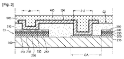
図1は、本発明の実施形態に従う太陽電池パネルを示す平面図である。図2は、第1セルC1及び第2セルC2が連結された状態を拡大して示す図である。図3は、図1のA−A’に沿って切断した断面を示す断面図である。 FIG. 1 is a plan view showing a solar cell panel according to an embodiment of the present invention. FIG. 2 is an enlarged view showing a state where the first cell C1 and the second cell C2 are connected. FIG. 3 is a cross-sectional view showing a cross section cut along A-A ′ of FIG. 1.
図1乃至図3を参照すると、実施形態に従う太陽電池パネルは、支持基板100、多数個のセルC1,C2...、第1絶縁フィルム310、第2絶縁フィルム320、多数個の接続部材400、メッキ層500、第1バスバー610、及び第2バスバー620を含む。
1 to 3, the solar cell panel according to the embodiment includes a
上記支持基板100は、上記セルC1,C2...、上記第1絶縁フィルム310、上記第2絶縁フィルム320、及び上記接続部材400を支持する。上記支持基板100はプレート形状を有し、フレキシブルである。
The
上記支持基板100は絶縁体である。上記支持基板100は、例えば、ステンレススチール基板またはエチレンビニールアセテート(ethylenevinylacetate;EVA)、またはポリイミド(polyimide;PI)などを含むポリマー基板でありうる。
The
上記セルC1,C2...は、上記支持基板100の上に配置される。上記セルC1,C2...は、互いに離隔してマトリックス形態に配置される。これとは異なり、上記セルC1,C2...は一方向に延びる形状を有することができ、ストライプ形態に配置される。
The cells C1, C2. . . Is disposed on the
上記セルC1,C2...は互いに直列または並列に連結される。より詳しくは、互いに離隔した上記セルC1,C2...は、上記接続部材400、上記第1バスバー610、及び上記第2バスバー620により互いに直列または並列に連結される。
The cells C1, C2. . . Are connected to each other in series or in parallel. More specifically, the cells C1, C2,. . . Are connected in series or in parallel by the connecting
上記セルC1,C2...は太陽光の入射を受けて電気エネルギーに変換させる。例えば、上記セルC1,C2...は、シリコン系太陽電池、CIGS系太陽電池のような半導体化合物系太陽電池及び染料感応太陽電池でありうる。 The cells C1, C2. . . Receives sunlight and converts it into electrical energy. For example, the cells C1, C2. . . Can be semiconductor compound solar cells such as silicon solar cells, CIGS solar cells and dye sensitive solar cells.
上記各々のセルC1,C2...は、後面電極210、光吸収部220、バッファ230、高抵抗バッファ240、及びウィンドウ250を含むことができる。
Each of the cells C1, C2. . . May include a
上記後面電極210は、上記支持基板100の上に配置される。上記後面電極210は導電層であり、上記後面電極210に使われる物質の例としては、モリブデンなどが挙げられる。
The
上記後面電極210は相対的に大きい面積を有する。即ち、上記後面電極210は、上記光吸収部220、上記バッファ230、上記高抵抗バッファ240、及び上記ウィンドウ250より大きい面積を有する。
The
これによって、上記後面電極210の上面の一部が露出する。即ち、上記後面電極210の一部は上記光吸収部220の側面に対して側方に突出する。
As a result, a part of the upper surface of the
上記光吸収部220は、上記後面電極層の上に配置される。上記光吸収部220は、上記ウィンドウ250を通じて入射される太陽光を吸収する。上記光吸収部220は、例えば、上記光吸収部220はI-III-VI族系化合物を含むことができる。例えば、上記光吸収部220は、銅−インジウム−ガリウム−セレナイド系(Cu(In,Ga)Se2;CIGS系)結晶構造、銅−インジウム−セレナイド系、または銅−ガリウム−セレナイド系結晶構造を有することができる。
The
上記光吸収部220のエネルギーバンドギャップ(band gap)は約1eV乃至1.8eVでありうる。
The
上記バッファ230は、上記光吸収部220の上に配置される。上記バッファ230は硫化カドミウム(CdS)を含み、上記バッファ230のエネルギーバンドギャップは約2.2eV乃至2.4eVである。
The
上記高抵抗バッファ240は、上記バッファ230の上に配置される。また、上記高抵抗バッファ240は、不純物がドーピングされていないジンクオキサイド(i−ZnO)を含む。上記高抵抗バッファ240のエネルギーバンドギャップは約3.1eV乃至3.3eVである。
The
上記ウィンドウ250は、上記高抵抗バッファ240の上に配置される。上記ウィンドウ250は透明で、導電層である。また、上記ウィンドウ250の抵抗は上記後面電極210の抵抗より高い。例えば、上記ウィンドウ250の抵抗は上記後面電極210の抵抗より約10倍乃至200倍大きいことがある。
The
上記ウィンドウ250はアルミニウムドーピングされたジンクオキサイド(Al doped zinc oxide;AZO)またはガリウムドーピングされたジンクオキサイド(Ga doped zinc oxide;GZO)などを含むことができる。上記ウィンドウ250の厚さは約800nm乃至約1200nmでありうる。
The
上記光吸収部220、上記バッファ230、上記高抵抗バッファ240、及び上記ウィンドウ250は、実質的に同一な面積を有することができる。この際、上記光吸収部220、上記バッファ230、上記高抵抗バッファ240、及び上記ウィンドウ250の面積は、上記後面電極210の面積より小さいことがある。
The
これによって、上記光吸収部220は上記後面電極210の上に階段形状を形成して積層される。即ち、上記光吸収部220は上記後面電極210と段差を形成することができる。上記バッファ230、上記高抵抗バッファ240、及び上記ウィンドウ層252は、上記後面電極210と段差を形成しない。即ち、上記光吸収部220、上記バッファ230、上記高抵抗バッファ240、及び上記ウィンドウ層252の外郭は互いに実質的に一致することができる。
Accordingly, the
上記後面電極210は、上記光吸収部220から露出する露出領域(OA)が形成される。即ち、上記露出領域(OA)は上記後面電極210の上面のうち、上記光吸収部220が配置されない領域である。
The
上記第1絶縁フィルム310は、上記支持基板100の上に配置される。上記第1絶縁フィルム310は、上記セルC1,C2...を覆う。より詳しくは、上記第1絶縁フィルム310は、上記セルC1,C2...の上に配置される。上記第1絶縁フィルム310は、上記セルC1,C2...の全体を覆うことができる。また、上記第1絶縁フィルム310は、上記セルC1,C2...及び上記支持基板100に密着する。
The first
上記第1絶縁フィルム310は透明で、絶縁体である。上記第1絶縁フィルム310に使われる物質の例としては、エチレンビニールアセテートなどが挙げられる。
The first
上記第1絶縁フィルム310には多数個の第1ビアホール311及び多数個の第2ビアホール312を含む。
The first
上記第1ビアホール311は上記第1絶縁フィルム310を貫通し、上記セルC1,C2...の一部を各々露出する。より詳しくは、上記第1ビアホール311は上記セルC1,C2...のウィンドウ250の上面を露出する。上記第1ビアホール311は、上記セルC1,C2...のウィンドウ250の外郭に対応して形成される。
The first via
上記第2ビアホール312は、上記第1絶縁フィルム310を貫通し、上記セルC1,C2...の他の一部を各々露出する。より詳しくは、上記第2ビアホール312は、上記セルC1,C2...の後面電極210の上面を露出する。より詳しくは、上記第2ビアホール312は上記露出領域(OA)に対応して形成される。
The second via
上記第2絶縁フィルム320は、上記第1絶縁フィルム310の上に配置される。上記第2絶縁フィルム320は、上記接続部材400、上記第1バスバー610、及び上記第2バスバー620を覆うことができる。上記第2絶縁フィルム320は、上記第1絶縁フィルム310の上面の全体を覆うことができる。
The second
また、上記第2絶縁フィルム320は、上記第1絶縁フィルム310に密着する。上記第2絶縁フィルム320は、上記セルC1,C2...、上記接続部材400、上記第1バスバー610、及び上記第2バスバー620を外部に対して密封することができる。
The second
上記第2絶縁フィルム320は透明で、絶縁体である。また、上記第2絶縁フィルム320はフレキシブルであり、高い耐久性を有することができる。また、上記第2絶縁フィルム320は、上記第1絶縁フィルム310と同一な物質で形成される。上記第2絶縁フィルム320に使われる物質の例としては、エチレンビニールアセテート、ポリイミド、またはポリエチレンテレフタレートなどが挙げられる。
The second
上記接続部材400は、上記セルC1,C2...の間に各々配置される。また、上記接続部材400は、上記第1絶縁基板の上、上記第1ビアホール311の内側、及び上記第2ビアホール312の内側に配置される。
The connecting
上記接続部材400は、上記セルC1,C2...を互いに連結させる。より詳しくは、上記接続部材400は隣り合うセルC1,C2...を連結させる。上記接続部材400は、上記第1ビアホール311及び上記第2ビアホール312を通じて隣り合うセルC1,C2...を連結させる。即ち、上記接続部材400は、上記第1ビアホール311及び上記第2ビアホール312を通じて上記セルC1,C2...に接続される。
The connecting
上記接続部材400は、上記セルC1,C2...を直列に連結させる。即ち、上記接続部材400は1つのセルのウィンドウ250を隣接するセルの後面電極210に連結させる。上記接続部材400は、上記第1ビアホール311及び上記第2ビアホール312を覆う。即ち、1つの接続部材400は1つの第1ビアホール311及び1つの第2ビアホール312を同時に覆う。
The connecting
上記接続部材400は導電体である。上記接続部材400は、例えば、導電性ペーストまたは導電テープでありうる。より詳しくは、上記接続部材400は、例えば、銀(Ag)ペーストまたは銅プレートでありうる。
The connecting
上記接続部材400はフレキシブルである。即ち、上記接続部材400は、上記支持基板100が撓むことによって湾曲される。
The connecting
上記接続部材400は、上記第1ビアホール311及び上記第2ビアホール312を通じて上記セルC1,C2...に各々連結される。即ち、上記接続部材400の一部は、上記第1ビアホール311及び上記第2ビアホール312の内側に配置されて、上記セルC1,C2...に接続される。
The
例えば、図1乃至図3に示すように、上記接続部材400のうちの1つは、第1セルC1及び第2セルC2を互いに直列に連結することができる。上記第1セルC1及び上記第2セルC2は互いに隣接して配置される。上記第1ビアホール311のうちの1つは、上記第1セルC1のウィンドウ251の一部を露出し、上記第2ビアホール312のうちの1つは上記第2セルC2の後面電極210の上面の一部を露出する。
For example, as illustrated in FIGS. 1 to 3, one of the
上記接続部材400は、上記第1ビアホール311を通じて上記第1セルC1のウィンドウ250に接続される。この際、上記接続部材400は上記第1セルC1のウィンドウ250に直接的な接触により接続される。
The
また、上記接続部材400は、上記第2ビアホール312を通じて上記第2セルC2の後面電極210の露出領域(OA)に接続される。この際、上記接続部材400は、上記第2セルC2の後面電極210に直接的な接触により接続される。
The
上記メッキ層500は上記接続部材400の周囲を囲む。また、上記メッキ層500は、上記第1ビアホール311により露出した上記セルC1,C2...のウィンドウ250の上に配置される。また、上記メッキ層500は上記第2ビアホール312に露出した上記セルC1,C2...の後面電極210の上面に配置される。また、上記メッキ層500は上記接続部材400及び上記セルC1,C2...のウィンドウ250の間に介される。また、上記メッキ層500は、上記接続部材400及び上記セルC1,C2...の後面電極210の間に介される。
The
上記接続部材400は、上記メッキ層500を通じて上記セルC1,C2...のウィンドウ250及び上記セルC1,C2...の後面電極210に接続される。即ち、上記メッキ層500は上記接続部材400及び上記セルC1,C2...のウィンドウ250の間に介されて、上記接続部材400及び上記セルC1,C2...のウィンドウ250の間の電気的及び機械的な接続特性を向上させる。同様に、上記メッキ層500は、上記接続部材400及び上記セルC1,C2...の後面電極210間に介されて、上記接続部材400及び上記セルC1,C2...のウィンドウ250の間の電気的及び機械的な特性を向上させる。
The
即ち、上記メッキ層500は、上記接続部材400、上記セルC1,C2...のウィンドウ250、及び上記セルC1,C2...の後面電極210にメッキされて形成される。
That is, the
上記メッキ層500は導電層であり、低い抵抗の金属を含むことができる。上記メッキ層500に使われる物質の例としては、銅、銀、または金などが挙げられる。
The
上記第1バスバー610は、上記セルC1,C2...を並列に連結する。より詳しくは、上記第1バスバー610は、外郭に配置されるセルC1,C2...の後面電極210に連結される。上記第1バスバー610は、上記第1絶縁フィルム310及び上記セルC1,C2...の後面電極210の間に配置される。上記第1バスバー610は延びる形状を有し、隣接する太陽電池パネルまたは外部の蓄電装置などに連結される。
The
上記第2バスバー620は、上記セルC1,C2...を並列に連結する。より詳しくは、上記第1バスバー610は、他の外郭に配置されるセルC1,C2...のウィンドウ250に連結される。上記第2バスバー620は、第1絶縁フィルム310及び上記セルC1,C2...のウィンドウ250の間に配置される。上記第2バスバー620は延びる形状を有し、隣接する太陽電池パネルまたは外部の蓄電装置などに連結される。
The
第1バスバー610及び第2バスバー620は導電体であり、上記第1バスバー610及び上記第2バスバー620に使われる物質の例としては、銅または銀などが挙げられる。上記バスバー及び上記第2バスバー620は、ペーストまたは導電テープ形態に製作される。
The
上記接続部材400は、隣接するセルC1,C2...を上記第1ビアホール311及び上記第2ビアホール312を通じて連結する。特に、上記接続部材400は、上記セルC1,C2...のウィンドウ250の上面及び後面電極210の上面に接続される。これによって、上記接続部材400はペーストなどがプリンティングされて形成される。
The connecting
即ち、上記接続部材400はプリンティング方式により形成されるので、実施形態に従う太陽光発電装置は、自動化工程などにより容易に製作できる。
That is, since the
また、上記接続部材400がプリンティングされた状態で、上記接続部材400及び上記セルC1,C2...に電気メッキにより上記メッキ層500が形成される。これによって、上記接続部材400は上記セルC1,C2...に固く接続され、実施形態に従う太陽電池パネルは断線などを防止する。
Further, in a state where the
また、上記メッキ層500によって、上記接続部材400及び上記セルC1,C2...の間の接続特性が向上し、実施形態に従う太陽電池パネルは、向上した電気的及び機械的な特性を有する。
Further, the connecting
したがって、実施形態に従う太陽電池パネルは容易に形成され、向上した信頼性を有する。 Therefore, the solar cell panel according to the embodiment is easily formed and has improved reliability.
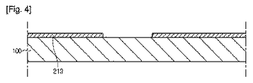
図4乃至図9は、本発明の実施形態に従う太陽電池パネルを製造する過程を示す図である。本製造方法に対する説明に、前述した太陽電池パネルに対する説明が本質的に結合できる。 4 to 9 are views showing a process of manufacturing the solar cell panel according to the embodiment of the present invention. The description of the solar cell panel described above can be essentially combined with the description of the manufacturing method.
図4を参照すると、支持基板100の上に多数個の後面電極210が形成される。
Referring to FIG. 4, a plurality of
上記後面電極210が形成されるために、上記支持基板100の上に後面電極層が形成される。上記後面電極層はスパッタリングなどの真空蒸着工程により上記支持基板100の上にモリブデンが蒸着されて形成される。
In order to form the
以後、上記後面電極層はレーザーなどによりパターニングされて、上記後面電極層は上記後面電極210に区分される。
Thereafter, the rear electrode layer is patterned by a laser or the like, and the rear electrode layer is divided into the
図5を参照すると、上記後面電極の上に、光吸収層221、バッファ層231、高抵抗バッファ層241、及びウィンドウ層252が形成される。
Referring to FIG. 5, a
上記光吸収層221はスパッタリング工程または蒸発法等により形成される。
The
例えば、上記光吸収層221を形成するために、銅、インジウム、ガリウム、セレニウムを同時または区分して蒸発させながら銅−インジウム−ガリウム−セレナイド系(Cu(In,Ga)Se2;CIGS系)の光吸収層221を形成する方法と、金属プリカーサ膜を形成させた後、セレン化(selenization)工程により形成させる方法が幅広く使われている。
For example, in order to form the
金属プリカーサ膜を形成させた後、セレン化することを細分化すれば、銅ターゲット、インジウムターゲット、ガリウムターゲットを使用するスパッタリング工程により、上記後面電極210の上に金属プリカーサ膜が形成される。
After forming the metal precursor film and subdividing the selenization, the metal precursor film is formed on the
以後、上記金属プリカーサ膜はセレン化(selenization)工程により、銅−インジウム−ガリウム−セレナイド系(Cu(In,Ga)Se2;CIGS系)の光吸収層221が形成される。
Thereafter, a copper-indium-gallium-selenide-based (Cu (In, Ga) Se 2 ; CIGS-based)
これとは異なり、上記銅ターゲット、インジウムターゲット、ガリウムターゲットを使用するスパッタリング工程及び上記セレン化工程は、同時に進行できる。 Unlike this, the sputtering process using the copper target, the indium target, and the gallium target and the selenization process can proceed simultaneously.
これとは異なり、銅ターゲット及びインジウムターゲットのみを使用したり、銅ターゲット及びガリウムターゲットを使用するスパッタリング工程及びセレン化工程により、CIS系またはCIG系光吸収層が形成される。 In contrast, a CIS-based or CIG-based light absorption layer is formed by a sputtering process and a selenization process using only a copper target and an indium target, or using a copper target and a gallium target.
以後、硫化カドミウムがスパッタリング工程または溶液成長法(chemical bath depositon;CBD)などにより蒸着され、上記バッファ層231が形成される。
Thereafter, cadmium sulfide is deposited by a sputtering process or a solution growth method (chemical bath depositon; CBD), and the
以後、上記バッファ層231の上にジンクオキサイドがスパッタリング工程などにより蒸着され、上記高抵抗バッファ層241が形成される。
Thereafter, zinc oxide is deposited on the
上記バッファ層231及び上記高抵抗バッファ層241は低い厚さで蒸着される。例えば、上記バッファ層231及び上記高抵抗バッファ層241の厚さは約1nm乃至約80nmである。
The
以後、上記高抵抗バッファ層241の上に透明な導電物質が蒸着されて上記ウィンドウ層252が形成される。例えば、上記ウィンドウ層252はアルミニウムがドーピングされたジンクオキサイドがスパッタリング工程により上記高抵抗バッファ層241の上に蒸着されて形成される。
Thereafter, a transparent conductive material is deposited on the high
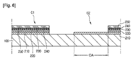
図6を参照すると、上記光吸収層221、上記バッファ層231、上記高抵抗バッファ層241、及び上記ウィンドウ層252は、レーザーまたは機械的なスクライビング等によりパターニングされる。より詳しくは、上記光吸収層221、上記バッファ層231、上記高抵抗バッファ層241、及び上記ウィンドウ層252は、一度にパターニングできる。これによって、多数個の光吸収部220、多数個のバッファ230、多数個の高抵抗バッファ240、及び多数個のウィンドウ250が形成される。
Referring to FIG. 6, the
これによって、上記支持基板100の上に、上記後面電極210、上記光吸収部220、上記バッファ230、上記高抵抗バッファ240、及び上記ウィンドウ250を含む多数個のセルC1,C2...が形成される。 As a result, a plurality of cells C1, C2,. . . Is formed.
この際、上記光吸収層221、上記バッファ層231、上記高抵抗バッファ層241、及び上記ウィンドウ層252は、上記後面電極210の上面の一部を露出するようにパターニングされる。これによって、上記後面電極210の上面には露出領域(OA)が形成される。
At this time, the
したがって、上記後面電極210及び上記光吸収部220は階段形状に積層される構造を有する。
Accordingly, the
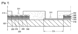
図7を参照すると、上記セルC1,C2...の上に第1絶縁フィルム310が形成される。即ち、上記セルC1,C2...が形成された支持基板100の上に上記第1絶縁フィルム310が合着される。以後、上記第1絶縁フィルム310には多数個の第1ビアホール311及び多数個の第2ビアホール312が形成される。
Referring to FIG. 7, the cells C1, C2,. . . A first insulating
上記第1ビアホール311は上記ウィンドウ250の上面を露出し、上記第2ビアホール312は上記後面電極210の露出領域(OA)を露出する。
The first via
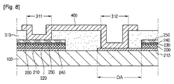
図8を参照すると、上記第1絶縁フィルム310の上に多数個の接続部材400が形成される。上記接続部材400はシルクスクリーン印刷などのプリンティング方式により形成される。
Referring to FIG. 8, a plurality of
即ち、金属粒子などの導電性粒子を含む導電性ペーストが上記セルC1,C2...の間にプリントされる。また、上記導電性ペーストは上記第1ビアホール311及び上記第2ビアホール312を覆うようにプリントされる。これによって、上記接続部材400が形成される。
That is, a conductive paste containing conductive particles such as metal particles is used for the cells C1, C2,. . . Will be printed during. The conductive paste is printed so as to cover the first via
以後、上記接続部材400は別に乾燥工程及び熱処理工程をさらに経ることができる。
Thereafter, the connecting
図9を参照すると、メッキ層500が形成され、上記第1絶縁フィルム310の上に第2絶縁フィルム320が形成される。
Referring to FIG. 9, a
上記メッキ層500は電気メッキにより形成される。例えば、上記接続部材400に負極が連結されて、電解質に含まれた銅イオンなどの金属イオンが上記接続部材400、露出したウィンドウ250、及び露出した後面電極210にメッキされる。
The
上記接続部材400は、上記後面電極210及び上記ウィンドウ250に完全に密着しないことがある。即ち、上記接続部材400の一部は上記後面電極210及び上記ウィンドウ250に直接接触されるが、上記接続部材400の他の一部は上記後面電極210及び上記ウィンドウ250と若干の空間を形成し、離隔する。
The
この際、上記接続部材400、上記後面電極210の上面、及び上記ウィンドウ250の上面に電気メッキによりメッキ層500が形成される。また、上記接続部材400及び上記後面電極210の間の若干の空間及び上記接続部材400及び上記ウィンドウ250の間の若干の空間に上記メッキ層500が形成される。
At this time, a
即ち、電解質に含まれた金属イオンは、上記接続部材400及び上記ウィンドウ250の間の空間及び上記接続部材400及び上記後面電極210の間の空間でもメッキできる。
That is, the metal ions contained in the electrolyte can be plated in the space between the
したがって、上記メッキ層500は、上記接続部材400及び上記ウィンドウ250の間、及び上記接続部材400及び上記後面電極210の間の電気的及び機械的な特性を向上させる。
Accordingly, the
このように、実施形態に従う太陽電池パネルは、上記接続部材400をプリンティング方式により一括的に形成することができる。また、上記メッキ層500によって、実施形態に従う太陽電池パネルは向上した特性を有する。
Thus, the solar cell panel according to the embodiment can collectively form the
以上、実施形態に説明された特徴、構造、効果などは、本発明の少なくとも1つの実施形態に含まれ、必ず1つの実施形態のみに限定されるものではない。延いては、各実施形態で例示された特徴、構造、効果などは、実施形態が属する分野の通常の知識を有する者により他の実施形態に対しても組合または変形されて実施可能である。したがって、このような組合と変形に関連した内容は本発明の範囲に含まれることと解釈されるべきである。 As described above, the features, structures, effects, and the like described in the embodiments are included in at least one embodiment of the present invention, and are not necessarily limited to only one embodiment. As a result, the features, structures, effects, and the like exemplified in each embodiment can be combined or modified with respect to other embodiments by a person having ordinary knowledge in the field to which the embodiment belongs. Therefore, contents related to such combinations and modifications should be construed as being included in the scope of the present invention.
以上、本発明を好ましい実施形態をもとに説明したが、これは単なる例示であり、本発明を限定するのでない。本発明の本質的な特性を逸脱しない範囲内で、多様な変形及び応用が可能であることが同業者にとって明らかである。例えば、実施形態に具体的に表れた各構成要素は変形して実施することができ、このような変形及び応用にかかわる差異点も、特許請求の範囲で規定する本発明の範囲に含まれるものと解釈されるべきである。 As mentioned above, although this invention was demonstrated based on preferable embodiment, this is only an illustration and does not limit this invention. It will be apparent to those skilled in the art that various modifications and applications can be made without departing from the essential characteristics of the invention. For example, each component specifically shown in the embodiment can be modified and implemented, and such differences in modification and application are also included in the scope of the present invention defined in the claims. Should be interpreted.
本発明に従う太陽光発電装置及びその製造方法は、太陽光発電分野に利用できる。 The solar power generation device and the manufacturing method thereof according to the present invention can be used in the field of solar power generation.
Claims (17)
前記基板の上に配置される第1セルと、
前記第1セルに隣接する第2セルと、
前記第1セル及び前記第2セルを覆う第1絶縁フィルムと、
前記第1セル及び前記第2セルを連結する接続部材と、を含み、
前記第1絶縁フィルムは、前記第1セルを露出する第1ビアホール及び前記第2セルを露出する第2ビアホールを含み、
前記接続部材は、前記第1ビアホール及び前記第2ビアホールを通じて、前記第1セル及び前記第2セルを連結することを特徴とする、太陽光発電装置。 A substrate,
A first cell disposed on the substrate;
A second cell adjacent to the first cell;
A first insulating film covering the first cell and the second cell;
A connecting member for connecting the first cell and the second cell;
The first insulating film includes a first via hole that exposes the first cell and a second via hole that exposes the second cell;
The solar power generation apparatus, wherein the connection member connects the first cell and the second cell through the first via hole and the second via hole.
前記基板の上に配置される第1後面電極と、
前記第1後面電極の上に配置される第1光吸収部と、
前記第1光吸収部の上に配置される第1ウィンドウと、を含み、
前記第2セルは、
前記基板の上に配置される第2後面電極と、
前記第2後面電極の上に配置される第2光吸収部と、
前記第2光吸収部の上に配置される第2ウィンドウと、を含み、
前記接続部材は、前記第1ウィンドウ及び前記第2後面電極を連結することを特徴とする請求項1に記載の太陽光発電装置。 The first cell is
A first rear electrode disposed on the substrate;
A first light absorber disposed on the first rear electrode;
A first window disposed on the first light absorption part,
The second cell is
A second rear electrode disposed on the substrate;
A second light absorber disposed on the second rear electrode;
A second window disposed on the second light absorber,
The solar power generation apparatus according to claim 1, wherein the connection member connects the first window and the second rear electrode.
前記基板の上に配置される第1セルと、
前記第1セルに隣接する第2セルと、
前記第1セル及び前記第2セルに連結される接続部材と、
前記接続部材の外部面にコーティングされるメッキ層と、
を含むことを特徴とする太陽光発電装置。 A substrate,
A first cell disposed on the substrate;
A second cell adjacent to the first cell;
A connecting member coupled to the first cell and the second cell;
A plating layer coated on the outer surface of the connection member;
A solar power generation device comprising:
前記第1絶縁フィルムは、前記第1セルを露出する第1ビアホール、及び前記第2セルを露出する第2ビアホールを含み、
前記接続部材は、前記第1ビアホール及び前記第2ビアホールを通じて、前記第1セル及び前記第2セルを連結することを特徴とする請求項9に記載の太陽光発電装置。 A first insulating film covering the first cell and the second cell;
The first insulating film includes a first via hole that exposes the first cell and a second via hole that exposes the second cell;
The photovoltaic power generation apparatus according to claim 9, wherein the connecting member connects the first cell and the second cell through the first via hole and the second via hole.
前記第1セル及び前記第2セルを各々露出する第1ビアホール及び第2ビアホールが形成される第1絶縁フィルムを形成するステップと、
前記第1ビアホール及び前記第2ビアホールを通じて前記第1セル及び前記第2セルに接続される接続部材を形成するステップと、
を含むことを特徴とする太陽光発電装置の製造方法。 Forming adjacent first and second cells on a substrate;
Forming a first insulating film in which a first via hole and a second via hole exposing the first cell and the second cell are formed; and
Forming a connection member connected to the first cell and the second cell through the first via hole and the second via hole;
The manufacturing method of the solar power generation device characterized by including.
Applications Claiming Priority (3)
| Application Number | Priority Date | Filing Date | Title |
|---|---|---|---|
| KR10-2010-0074417 | 2010-07-30 | ||
| KR1020100074417A KR101114099B1 (en) | 2010-07-30 | 2010-07-30 | Solar cell apparatus and method of fabricating the same |
| PCT/KR2011/003124 WO2012015150A1 (en) | 2010-07-30 | 2011-04-27 | Device for generating photovoltaic power and method for manufacturing same |
Publications (2)
| Publication Number | Publication Date |
|---|---|
| JP2013532907A true JP2013532907A (en) | 2013-08-19 |
| JP2013532907A5 JP2013532907A5 (en) | 2014-07-17 |
Family
ID=45530315
Family Applications (1)
| Application Number | Title | Priority Date | Filing Date |
|---|---|---|---|
| JP2013521675A Pending JP2013532907A (en) | 2010-07-30 | 2011-04-27 | Photovoltaic power generation apparatus and manufacturing method thereof |
Country Status (6)
| Country | Link |
|---|---|
| US (1) | US9391215B2 (en) |
| EP (1) | EP2511961A4 (en) |
| JP (1) | JP2013532907A (en) |
| KR (1) | KR101114099B1 (en) |
| CN (1) | CN103201854A (en) |
| WO (1) | WO2012015150A1 (en) |
Families Citing this family (5)
| Publication number | Priority date | Publication date | Assignee | Title |
|---|---|---|---|---|
| EP2757593B1 (en) * | 2013-01-17 | 2018-10-17 | ATOTECH Deutschland GmbH | Plated electrical contacts for solar modules |
| US9640331B2 (en) * | 2013-03-22 | 2017-05-02 | Sharp Laboratories Of America, Inc. | Solid state dye-sensitized solar cell tandem module |
| US20150037915A1 (en) * | 2013-07-31 | 2015-02-05 | Wei-Sheng Lei | Method and system for laser focus plane determination in a laser scribing process |
| WO2020205636A1 (en) * | 2019-03-29 | 2020-10-08 | Sunpower Corporation | Solar cells having hybrid architectures including differentiated p-type and n-type regions with offset contacts |
| EP4318604A1 (en) | 2022-08-04 | 2024-02-07 | Solertix Srl | Thin film photovoltaic devices and method of manufacturing them |
Citations (4)
| Publication number | Priority date | Publication date | Assignee | Title |
|---|---|---|---|---|
| JPS6035553A (en) * | 1984-06-26 | 1985-02-23 | Sharp Corp | Thin film solar cell device |
| JPH04116986A (en) * | 1990-09-07 | 1992-04-17 | Canon Inc | Integrated solar cell and manufacture of the same |
| JPH0818082A (en) * | 1994-07-05 | 1996-01-19 | Fuji Electric Co Ltd | Manufacture of flexible solar cell module |
| JP2000196116A (en) * | 1998-12-28 | 2000-07-14 | Sony Corp | Integrated thin-film element and its manufacture |
Family Cites Families (14)
| Publication number | Priority date | Publication date | Assignee | Title |
|---|---|---|---|---|
| CA2024662A1 (en) * | 1989-09-08 | 1991-03-09 | Robert Oswald | Monolithic series and parallel connected photovoltaic module |
| JP2001119043A (en) * | 1999-10-14 | 2001-04-27 | Sony Corp | Equipment for manufacturing semiconductor element |
| JP2001284617A (en) * | 2000-03-29 | 2001-10-12 | Citizen Watch Co Ltd | Solar cell, its manufacturing method and watch using the same |
| JP2002319686A (en) | 2001-04-23 | 2002-10-31 | Matsushita Electric Ind Co Ltd | Method of manufacturing integrated thin film solar battery |
| AUPR719701A0 (en) * | 2001-08-23 | 2001-09-13 | Pacific Solar Pty Limited | Chain link metal interconnect structure |
| KR20070050597A (en) * | 2005-11-11 | 2007-05-16 | 조봉운 | Solar cell module and manufacturing method thereof |
| JP2007305876A (en) | 2006-05-12 | 2007-11-22 | Matsushita Electric Ind Co Ltd | Solar cell module |
| US20090145472A1 (en) * | 2007-12-10 | 2009-06-11 | Terra Solar Global, Inc. | Photovoltaic devices having conductive paths formed through the active photo absorber |
| DE212008000087U1 (en) * | 2007-12-14 | 2010-08-12 | Miasole, Santa Clara | Photovoltaic, environmentally protected facility |
| KR100953618B1 (en) | 2008-01-11 | 2010-04-20 | 삼성에스디아이 주식회사 | Solar cell |
| KR100927725B1 (en) | 2008-01-25 | 2009-11-18 | 삼성에스디아이 주식회사 | Solar cell and manufacturing method thereof |
| JP2009259926A (en) * | 2008-04-15 | 2009-11-05 | Mitsubishi Electric Corp | Solar cell |
| DE102008060404A1 (en) * | 2008-07-30 | 2010-02-11 | Helmholtz-Zentrum Berlin Für Materialien Und Energie Gmbh | Single-sided contacted thin-film solar module with an inner contact layer |
| US20110120545A1 (en) * | 2009-11-20 | 2011-05-26 | E. I. Du Pont De Nemours And Company | Photovoltaic compositions or precursors thereto, and methods relating thereto |
-
2010
- 2010-07-30 KR KR1020100074417A patent/KR101114099B1/en not_active IP Right Cessation
-
2011
- 2011-04-27 CN CN201180037336XA patent/CN103201854A/en active Pending
- 2011-04-27 WO PCT/KR2011/003124 patent/WO2012015150A1/en active Application Filing
- 2011-04-27 US US13/813,248 patent/US9391215B2/en not_active Expired - Fee Related
- 2011-04-27 EP EP11812681.2A patent/EP2511961A4/en not_active Withdrawn
- 2011-04-27 JP JP2013521675A patent/JP2013532907A/en active Pending
Patent Citations (4)
| Publication number | Priority date | Publication date | Assignee | Title |
|---|---|---|---|---|
| JPS6035553A (en) * | 1984-06-26 | 1985-02-23 | Sharp Corp | Thin film solar cell device |
| JPH04116986A (en) * | 1990-09-07 | 1992-04-17 | Canon Inc | Integrated solar cell and manufacture of the same |
| JPH0818082A (en) * | 1994-07-05 | 1996-01-19 | Fuji Electric Co Ltd | Manufacture of flexible solar cell module |
| JP2000196116A (en) * | 1998-12-28 | 2000-07-14 | Sony Corp | Integrated thin-film element and its manufacture |
Also Published As
| Publication number | Publication date |
|---|---|
| WO2012015150A1 (en) | 2012-02-02 |
| KR20120012327A (en) | 2012-02-09 |
| EP2511961A4 (en) | 2013-12-11 |
| CN103201854A (en) | 2013-07-10 |
| US9391215B2 (en) | 2016-07-12 |
| EP2511961A1 (en) | 2012-10-17 |
| KR101114099B1 (en) | 2012-02-22 |
| US20130180566A1 (en) | 2013-07-18 |
Similar Documents
| Publication | Publication Date | Title |
|---|---|---|
| US20120174977A1 (en) | Solar Power Generation Apparatus and Manufacturing Method Thereof | |
| JP2013510426A (en) | Solar cell and manufacturing method thereof | |
| JP2013507766A (en) | Photovoltaic power generation apparatus and manufacturing method thereof | |
| US9553213B2 (en) | Solar cell apparatus and method of fabricating the same | |
| JP2014504035A (en) | Photovoltaic power generation apparatus and manufacturing method thereof. | |
| US9941424B2 (en) | Solar cell | |
| JP2013532907A (en) | Photovoltaic power generation apparatus and manufacturing method thereof | |
| JP2012532442A (en) | Solar cell and manufacturing method thereof | |
| KR101283072B1 (en) | Solar cell apparatus and method of fabricating the same | |
| JP5840213B2 (en) | Photovoltaic power generation apparatus and manufacturing method thereof | |
| KR101428146B1 (en) | Solar cell module and method of fabricating the same | |
| KR101114169B1 (en) | Solar cell apparatus | |
| JP2013532911A (en) | Photovoltaic power generation apparatus and manufacturing method thereof | |
| JP5624153B2 (en) | Solar cell and manufacturing method thereof | |
| JP2013516784A (en) | Photovoltaic power generation apparatus and manufacturing method thereof | |
| JP2014503128A (en) | Solar cell and manufacturing method thereof | |
| KR101251841B1 (en) | Solar cell apparatus and method of fabricating the same | |
| EP2450966A2 (en) | Solar battery and a production method for same | |
| KR20110001792A (en) | Solar cell and mehtod of fabricating the same | |
| KR20130119072A (en) | Photovoltaic apparatus | |
| JP2013536996A (en) | Photovoltaic power generation apparatus and manufacturing method thereof | |
| KR20100109310A (en) | Solar cell and method of fabricating the same | |
| KR101326885B1 (en) | Solar cell and method of fabricating the same | |
| KR101081222B1 (en) | Solar cell aparatus | |
| JP2013522926A (en) | Photovoltaic power generation apparatus and manufacturing method thereof |
Legal Events
| Date | Code | Title | Description |
|---|---|---|---|
| A621 | Written request for application examination |
Free format text: JAPANESE INTERMEDIATE CODE: A621 Effective date: 20140428 |
|
| A521 | Request for written amendment filed |
Free format text: JAPANESE INTERMEDIATE CODE: A523 Effective date: 20140530 |
|
| A131 | Notification of reasons for refusal |
Free format text: JAPANESE INTERMEDIATE CODE: A131 Effective date: 20140930 |
|
| A977 | Report on retrieval |
Free format text: JAPANESE INTERMEDIATE CODE: A971007 Effective date: 20140930 |
|
| A02 | Decision of refusal |
Free format text: JAPANESE INTERMEDIATE CODE: A02 Effective date: 20150303 |