JP2013102417A - クロック分配回路 - Google Patents
クロック分配回路 Download PDFInfo
- Publication number
- JP2013102417A JP2013102417A JP2012172302A JP2012172302A JP2013102417A JP 2013102417 A JP2013102417 A JP 2013102417A JP 2012172302 A JP2012172302 A JP 2012172302A JP 2012172302 A JP2012172302 A JP 2012172302A JP 2013102417 A JP2013102417 A JP 2013102417A
- Authority
- JP
- Japan
- Prior art keywords
- clock
- circuit
- branch point
- generation circuit
- signal
- Prior art date
- Legal status (The legal status is an assumption and is not a legal conclusion. Google has not performed a legal analysis and makes no representation as to the accuracy of the status listed.)
- Pending
Links
Images


Classifications
-
- G—PHYSICS
- G06—COMPUTING OR CALCULATING; COUNTING
- G06F—ELECTRIC DIGITAL DATA PROCESSING
- G06F1/00—Details not covered by groups G06F3/00 - G06F13/00 and G06F21/00
- G06F1/04—Generating or distributing clock signals or signals derived directly therefrom
- G06F1/10—Distribution of clock signals, e.g. skew
Landscapes
- Engineering & Computer Science (AREA)
- Theoretical Computer Science (AREA)
- Physics & Mathematics (AREA)
- General Engineering & Computer Science (AREA)
- General Physics & Mathematics (AREA)
- Design And Manufacture Of Integrated Circuits (AREA)
- Semiconductor Integrated Circuits (AREA)
- Manipulation Of Pulses (AREA)
Priority Applications (2)
| Application Number | Priority Date | Filing Date | Title |
|---|---|---|---|
| JP2012172302A JP2013102417A (ja) | 2011-10-14 | 2012-08-02 | クロック分配回路 |
| US13/597,366 US8710892B2 (en) | 2011-10-14 | 2012-08-29 | Clock distribution circuit |
Applications Claiming Priority (3)
| Application Number | Priority Date | Filing Date | Title |
|---|---|---|---|
| JP2011227436 | 2011-10-14 | ||
| JP2011227436 | 2011-10-14 | ||
| JP2012172302A JP2013102417A (ja) | 2011-10-14 | 2012-08-02 | クロック分配回路 |
Publications (2)
| Publication Number | Publication Date |
|---|---|
| JP2013102417A true JP2013102417A (ja) | 2013-05-23 |
| JP2013102417A5 JP2013102417A5 (cg-RX-API-DMAC7.html) | 2015-08-06 |
Family
ID=48085584
Family Applications (1)
| Application Number | Title | Priority Date | Filing Date |
|---|---|---|---|
| JP2012172302A Pending JP2013102417A (ja) | 2011-10-14 | 2012-08-02 | クロック分配回路 |
Country Status (2)
| Country | Link |
|---|---|
| US (1) | US8710892B2 (cg-RX-API-DMAC7.html) |
| JP (1) | JP2013102417A (cg-RX-API-DMAC7.html) |
Families Citing this family (2)
| Publication number | Priority date | Publication date | Assignee | Title |
|---|---|---|---|---|
| US9793900B1 (en) | 2016-06-29 | 2017-10-17 | Microsoft Technology Licensing, Llc | Distributed multi-phase clock generator having coupled delay-locked loops |
| US10585449B1 (en) * | 2019-01-15 | 2020-03-10 | Arm Limited | Clock circuitry for functionally safe systems |
Citations (5)
| Publication number | Priority date | Publication date | Assignee | Title |
|---|---|---|---|---|
| JPH06282350A (ja) * | 1993-01-27 | 1994-10-07 | Hitachi Ltd | Lsi内クロック分配回路 |
| JP2002023886A (ja) * | 2000-07-11 | 2002-01-25 | Nec Corp | 半導体集積回路 |
| US6429715B1 (en) * | 2000-01-13 | 2002-08-06 | Xilinx, Inc. | Deskewing clock signals for off-chip devices |
| US20040080347A1 (en) * | 2002-05-02 | 2004-04-29 | Wong Keng L. | Voltage ID based frequency control for clock generating circuit |
| JP2007336003A (ja) * | 2006-06-12 | 2007-12-27 | Nec Electronics Corp | クロック分配回路、半導体集積回路、クロック分配回路の形成方法及びそのプログラム |
Family Cites Families (2)
| Publication number | Priority date | Publication date | Assignee | Title |
|---|---|---|---|---|
| US6839301B2 (en) * | 2003-04-28 | 2005-01-04 | Micron Technology, Inc. | Method and apparatus for improving stability and lock time for synchronous circuits |
| JP2008010607A (ja) | 2006-06-29 | 2008-01-17 | Nec Computertechno Ltd | 半導体集積回路およびクロックスキュー低減方法 |
-
2012
- 2012-08-02 JP JP2012172302A patent/JP2013102417A/ja active Pending
- 2012-08-29 US US13/597,366 patent/US8710892B2/en active Active
Patent Citations (5)
| Publication number | Priority date | Publication date | Assignee | Title |
|---|---|---|---|---|
| JPH06282350A (ja) * | 1993-01-27 | 1994-10-07 | Hitachi Ltd | Lsi内クロック分配回路 |
| US6429715B1 (en) * | 2000-01-13 | 2002-08-06 | Xilinx, Inc. | Deskewing clock signals for off-chip devices |
| JP2002023886A (ja) * | 2000-07-11 | 2002-01-25 | Nec Corp | 半導体集積回路 |
| US20040080347A1 (en) * | 2002-05-02 | 2004-04-29 | Wong Keng L. | Voltage ID based frequency control for clock generating circuit |
| JP2007336003A (ja) * | 2006-06-12 | 2007-12-27 | Nec Electronics Corp | クロック分配回路、半導体集積回路、クロック分配回路の形成方法及びそのプログラム |
Also Published As
| Publication number | Publication date |
|---|---|
| US8710892B2 (en) | 2014-04-29 |
| US20130093476A1 (en) | 2013-04-18 |
Similar Documents
| Publication | Publication Date | Title |
|---|---|---|
| US7809971B2 (en) | Clock distribution circuit, semiconductor integrated circuit and method of designing clock distribution circuit | |
| CN101467115B (zh) | 集成电路及其上的存储器接口电路和使用集成电路从存储器读取数据的方法 | |
| JP5798442B2 (ja) | クロック分配回路及びクロック分配回路の形成方法 | |
| CN103258561B (zh) | 半导体装置的数据输出定时控制电路 | |
| US8058925B2 (en) | Adaptive temporal filtering of single event effects | |
| KR100477808B1 (ko) | 듀티 사이클 교정이 가능한 디지털 디엘엘 장치 및 듀티사이클 교정 방법 | |
| US9553595B2 (en) | Clock operation method and circuit | |
| US8766688B2 (en) | DLL circuit and delay-locked method using the same | |
| US9898035B2 (en) | Clock synchronization method | |
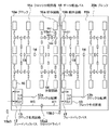
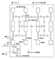
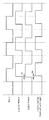
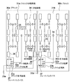
| JP2013102417A (ja) | クロック分配回路 | |
| US20020073389A1 (en) | Clock tuning circuit in chip design | |
| TW558872B (en) | Delay-locked loop device and method for generating clock signal | |
| US7102408B2 (en) | Information processing apparatus with adjustable system clock | |
| US7181709B2 (en) | Clock delay adjusting method of semiconductor integrated circuit device and semiconductor integrated circuit device formed by the method | |
| JP2010233018A (ja) | クロック分配回路及びクロックスキュー調整方法 | |
| JP2008140821A (ja) | 半導体装置および半導体装置の設計方法 | |
| JP2013102417A5 (cg-RX-API-DMAC7.html) | ||
| KR100838376B1 (ko) | 전원전압 변동에 대비한 디엘엘장치. | |
| JP2005044854A (ja) | クロックツリー回路、半導体集積回路装置、半導体集積回路装置の設計方法、および、半導体集積回路の設計プログラムを記録した媒体 | |
| JP3415516B2 (ja) | Pll回路及び半導体集積回路 | |
| JP4425300B2 (ja) | 半導体集積回路装置の設計プログラム、および、記録媒体 | |
| KR20040072083A (ko) | 클럭 신호의 스큐를 감소시키는 다중 위상 클럭 발생회로및 이에 대한 다중위상 클럭 발생방법 | |
| JP2009187110A (ja) | クロック分配回路の設計方法 | |
| JP2025140994A (ja) | 信号出力回路及び集積回路 | |
| KR20080001124A (ko) | 반도체 메모리 장치 |
Legal Events
| Date | Code | Title | Description |
|---|---|---|---|
| A521 | Written amendment |
Free format text: JAPANESE INTERMEDIATE CODE: A523 Effective date: 20150622 |
|
| A621 | Written request for application examination |
Free format text: JAPANESE INTERMEDIATE CODE: A621 Effective date: 20150622 |
|
| A977 | Report on retrieval |
Free format text: JAPANESE INTERMEDIATE CODE: A971007 Effective date: 20160224 |
|
| A131 | Notification of reasons for refusal |
Free format text: JAPANESE INTERMEDIATE CODE: A131 Effective date: 20160229 |
|
| A521 | Written amendment |
Free format text: JAPANESE INTERMEDIATE CODE: A523 Effective date: 20160502 |
|
| A02 | Decision of refusal |
Free format text: JAPANESE INTERMEDIATE CODE: A02 Effective date: 20160715 |