JP2012106901A - 積層セラミックス電子部品用セラミックスグリーンシートの製造方法及びこれを利用した積層セラミックス電子部品用セラミックスグリーンシート - Google Patents
積層セラミックス電子部品用セラミックスグリーンシートの製造方法及びこれを利用した積層セラミックス電子部品用セラミックスグリーンシート Download PDFInfo
- Publication number
- JP2012106901A JP2012106901A JP2011037988A JP2011037988A JP2012106901A JP 2012106901 A JP2012106901 A JP 2012106901A JP 2011037988 A JP2011037988 A JP 2011037988A JP 2011037988 A JP2011037988 A JP 2011037988A JP 2012106901 A JP2012106901 A JP 2012106901A
- Authority
- JP
- Japan
- Prior art keywords
- green sheet
- ceramic green
- coating layer
- substrate
- surface energy
- Prior art date
- Legal status (The legal status is an assumption and is not a legal conclusion. Google has not performed a legal analysis and makes no representation as to the accuracy of the status listed.)
- Pending
Links
- 239000000919 ceramic Substances 0.000 title claims abstract description 187
- 238000004519 manufacturing process Methods 0.000 title claims abstract description 36
- 238000000034 method Methods 0.000 title claims abstract description 29
- 239000011247 coating layer Substances 0.000 claims abstract description 92
- 239000000463 material Substances 0.000 claims abstract description 44
- 239000000758 substrate Substances 0.000 claims description 60
- -1 polyethylene terephthalate Polymers 0.000 claims description 25
- 229920001296 polysiloxane Polymers 0.000 claims description 10
- 229920000139 polyethylene terephthalate Polymers 0.000 claims description 9
- 239000005020 polyethylene terephthalate Substances 0.000 claims description 9
- 239000004698 Polyethylene Substances 0.000 claims description 8
- 239000004743 Polypropylene Substances 0.000 claims description 8
- 229920000573 polyethylene Polymers 0.000 claims description 8
- 229920001155 polypropylene Polymers 0.000 claims description 8
- 238000010030 laminating Methods 0.000 claims description 3
- 230000007547 defect Effects 0.000 abstract description 20
- 239000003985 ceramic capacitor Substances 0.000 abstract description 17
- 230000002950 deficient Effects 0.000 abstract description 3
- 239000000126 substance Substances 0.000 abstract description 3
- 239000002002 slurry Substances 0.000 description 14
- 239000010410 layer Substances 0.000 description 7
- 239000000843 powder Substances 0.000 description 5
- 239000011230 binding agent Substances 0.000 description 3
- 230000000052 comparative effect Effects 0.000 description 3
- 230000006866 deterioration Effects 0.000 description 3
- 238000010586 diagram Methods 0.000 description 3
- 238000001035 drying Methods 0.000 description 3
- 238000000926 separation method Methods 0.000 description 3
- 239000011248 coating agent Substances 0.000 description 2
- 238000000576 coating method Methods 0.000 description 2
- 230000007423 decrease Effects 0.000 description 2
- 239000010408 film Substances 0.000 description 2
- 238000010304 firing Methods 0.000 description 2
- 238000007639 printing Methods 0.000 description 2
- 239000004447 silicone coating Substances 0.000 description 2
- 239000007787 solid Substances 0.000 description 2
- OKKJLVBELUTLKV-UHFFFAOYSA-N Methanol Chemical group OC OKKJLVBELUTLKV-UHFFFAOYSA-N 0.000 description 1
- 239000004372 Polyvinyl alcohol Substances 0.000 description 1
- 239000000853 adhesive Substances 0.000 description 1
- 230000001070 adhesive effect Effects 0.000 description 1
- JRPBQTZRNDNNOP-UHFFFAOYSA-N barium titanate Chemical compound [Ba+2].[Ba+2].[O-][Ti]([O-])([O-])[O-] JRPBQTZRNDNNOP-UHFFFAOYSA-N 0.000 description 1
- 229910002113 barium titanate Inorganic materials 0.000 description 1
- 230000015572 biosynthetic process Effects 0.000 description 1
- 239000004020 conductor Substances 0.000 description 1
- 230000008878 coupling Effects 0.000 description 1
- 238000010168 coupling process Methods 0.000 description 1
- 238000005859 coupling reaction Methods 0.000 description 1
- 230000003247 decreasing effect Effects 0.000 description 1
- 230000000694 effects Effects 0.000 description 1
- 239000000446 fuel Substances 0.000 description 1
- 229920000609 methyl cellulose Polymers 0.000 description 1
- 239000001923 methylcellulose Substances 0.000 description 1
- 235000010981 methylcellulose Nutrition 0.000 description 1
- 229920000058 polyacrylate Polymers 0.000 description 1
- 229920002451 polyvinyl alcohol Polymers 0.000 description 1
- 230000008707 rearrangement Effects 0.000 description 1
- 238000007650 screen-printing Methods 0.000 description 1
- 239000002904 solvent Substances 0.000 description 1
- 239000010409 thin film Substances 0.000 description 1
Images

Classifications
-
- H—ELECTRICITY
- H01—ELECTRIC ELEMENTS
- H01G—CAPACITORS; CAPACITORS, RECTIFIERS, DETECTORS, SWITCHING DEVICES, LIGHT-SENSITIVE OR TEMPERATURE-SENSITIVE DEVICES OF THE ELECTROLYTIC TYPE
- H01G4/00—Fixed capacitors; Processes of their manufacture
- H01G4/002—Details
- H01G4/018—Dielectrics
- H01G4/06—Solid dielectrics
- H01G4/08—Inorganic dielectrics
- H01G4/12—Ceramic dielectrics
-
- H—ELECTRICITY
- H01—ELECTRIC ELEMENTS
- H01G—CAPACITORS; CAPACITORS, RECTIFIERS, DETECTORS, SWITCHING DEVICES, LIGHT-SENSITIVE OR TEMPERATURE-SENSITIVE DEVICES OF THE ELECTROLYTIC TYPE
- H01G4/00—Fixed capacitors; Processes of their manufacture
- H01G4/30—Stacked capacitors
-
- H—ELECTRICITY
- H03—ELECTRONIC CIRCUITRY
- H03H—IMPEDANCE NETWORKS, e.g. RESONANT CIRCUITS; RESONATORS
- H03H1/00—Constructional details of impedance networks whose electrical mode of operation is not specified or applicable to more than one type of network
- H03H2001/0021—Constructional details
- H03H2001/0085—Multilayer, e.g. LTCC, HTCC, green sheets
Landscapes
- Engineering & Computer Science (AREA)
- Power Engineering (AREA)
- Chemical & Material Sciences (AREA)
- Manufacturing & Machinery (AREA)
- Microelectronics & Electronic Packaging (AREA)
- Ceramic Engineering (AREA)
- Inorganic Chemistry (AREA)
- Ceramic Capacitors (AREA)
- Fixed Capacitors And Capacitor Manufacturing Machines (AREA)
- Compositions Of Oxide Ceramics (AREA)
Abstract
【解決手段】本発明の一実施形態による積層セラミックス電子部品用セラミックスグリーンシートは、基材上に形成され、基材に比べて表面エネルギーが低いコーティング層、及びコーティング層を覆うように形成され、前記コーティング層よりも表面エネルギーが高いセラミックスグリーンシートを含む。
【選択図】図2a
Description
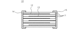
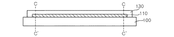
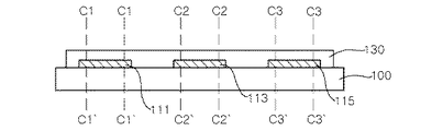
11 複数の誘電体シート
12、13 第1及び第2内部電極
14、15 第1及び第2外部電極
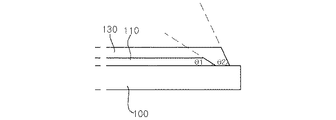
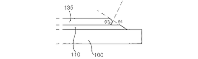
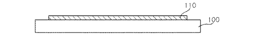
100 基材
110 コーティング層
111、113、115 第1コーティング層、第2コーティング層、第3コーティング層
130、135 セラミックスグリーンシート
C−C' 切断ライン
Claims (12)
- 積層セラミックス電子部品用セラミックスグリーンシートを製造するための基材、
前記基材上に形成され、前記基材に比べて表面エネルギーが低いコーティング層、及び、
前記コーティング層を覆うように形成され、前記コーティング層よりも表面エネルギーが高いセラミックスグリーンシート、
を含む積層セラミックス電子部品用セラミックスグリーンシート。 - 前記コーティング層はシリコーン(Si)を含む請求項1に記載の積層セラミックス電子部品用セラミックスグリーンシート。
- 前記コーティング層は前記基材上に部分的に形成される請求項1に記載の積層セラミックス電子部品用セラミックスグリーンシート。
- 前記基材は、ポリエチレンテレフタレート(Polyethylene terephthalate)、ポリプロピレン(polypropylnene)、またはポリエチレン(polyethylene)を含む請求項1に記載の積層セラミックス電子部品用セラミックスグリーンシート。
- 基材上に基材に比べて表面エネルギーが低いコーティング層を形成する段階、及び、
前記コーティング層を覆うように、前記コーティング層よりも表面エネルギーが高いセラミックスグリーンシートを形成する段階、
を含む積層セラミックス電子部品用セラミックスグリーンシートの製造方法。 - 前記コーティング層はシリコーン(Si)を含む請求項5に記載の積層セラミックス電子部品用セラミックスグリーンシートの製造方法。
- 前記コーティング層は基材上に部分的に形成される請求項5に記載の積層セラミックス電子部品用セラミックスグリーンシートの製造方法。
- 前記基材は、ポリエチレンテレフタレート(polyethylene terephthalate)、ポリプロピレン(polypropylnene)、またはポリエチレン(polyethylene)を含む請求項5に記載の積層セラミックス電子部品用セラミックスグリーンシートの製造方法。
- 基材上に基材に比べて表面エネルギーが低いコーティング層を形成する段階、
前記コーティング層を覆うように、前記コーティング層よりも表面エネルギーが高いセラミックスグリーンシートを形成する段階、
セラミックスグリーンシート、コーティング層及び基材を含むようにセラミックスグリーンシートを切断する段階、及び、
基材とコーティング層から切断されたセラミックスグリーンシートを分離し、前記切断されたセラミックスグリーンシートを積層する段階、
を含む積層セラミックス電子部品の製造方法。 - 前記コーティング層はシリコーン(Si)を含む請求項9に記載の積層セラミックス電子部品の製造方法。
- 前記コーティング層は基材上に部分的に形成される請求項9に記載の積層セラミックス電子部品の製造方法。
- 前記基材は、ポリエチレンテレフタレート(polyethylene terephthalate)、ポリプロピレン(polypropylnene)、またはポリエチレン(polyethylene)を含む請求項9に記載の積層セラミックス電子部品の製造方法。
Applications Claiming Priority (2)
| Application Number | Priority Date | Filing Date | Title |
|---|---|---|---|
| KR10-2010-0114139 | 2010-11-16 | ||
| KR1020100114139A KR20120052820A (ko) | 2010-11-16 | 2010-11-16 | 적층 세라믹 전자부품용 세라믹 그린시트 제조방법 및 이를 이용한 적층 세라믹 전자부품용 세라믹 그린시트 |
Publications (1)
| Publication Number | Publication Date |
|---|---|
| JP2012106901A true JP2012106901A (ja) | 2012-06-07 |
Family
ID=46269321
Family Applications (1)
| Application Number | Title | Priority Date | Filing Date |
|---|---|---|---|
| JP2011037988A Pending JP2012106901A (ja) | 2010-11-16 | 2011-02-24 | 積層セラミックス電子部品用セラミックスグリーンシートの製造方法及びこれを利用した積層セラミックス電子部品用セラミックスグリーンシート |
Country Status (2)
| Country | Link |
|---|---|
| JP (1) | JP2012106901A (ja) |
| KR (1) | KR20120052820A (ja) |
Citations (2)
| Publication number | Priority date | Publication date | Assignee | Title |
|---|---|---|---|---|
| JPH0837381A (ja) * | 1994-07-21 | 1996-02-06 | Hitachi Chem Co Ltd | 端子付多層配線板の製造法 |
| JP2002121075A (ja) * | 2000-10-06 | 2002-04-23 | Murata Mfg Co Ltd | セラミックグリーンシート及び積層セラミック電子部品の製造方法 |
-
2010
- 2010-11-16 KR KR1020100114139A patent/KR20120052820A/ko not_active Withdrawn
-
2011
- 2011-02-24 JP JP2011037988A patent/JP2012106901A/ja active Pending
Patent Citations (2)
| Publication number | Priority date | Publication date | Assignee | Title |
|---|---|---|---|---|
| JPH0837381A (ja) * | 1994-07-21 | 1996-02-06 | Hitachi Chem Co Ltd | 端子付多層配線板の製造法 |
| JP2002121075A (ja) * | 2000-10-06 | 2002-04-23 | Murata Mfg Co Ltd | セラミックグリーンシート及び積層セラミック電子部品の製造方法 |
Also Published As
| Publication number | Publication date |
|---|---|
| KR20120052820A (ko) | 2012-05-24 |
Similar Documents
| Publication | Publication Date | Title |
|---|---|---|
| CN1307668C (zh) | 陶瓷电子元件的制造方法 | |
| TWI500056B (zh) | 多層陶瓷電容器及用於多層陶瓷電容器的安裝板件 | |
| TWI453777B (zh) | 積層晶片電子元件、用於嵌裝該積層晶片電子元件之板體,及其封裝單元 | |
| KR101275426B1 (ko) | 내부전극용 도전성 페이스트 조성물, 이를 포함하는 적층 세라믹 커패시터 및 이의 제조방법 | |
| JP2013149939A (ja) | 積層セラミック電子部品及びその製造方法 | |
| JP2013149936A (ja) | 積層セラミック電子部品及びその製造方法 | |
| JP2011124571A (ja) | 外部電極用導電性ペースト組成物、これを含む積層セラミックキャパシタ及びその製造方法 | |
| US7799409B2 (en) | Ceramic green sheet structure and method for manufacturing laminated ceramic electronic component | |
| KR20120054843A (ko) | 전극 형성 장치 및 이를 이용한 전극 형성 방법 | |
| CN111312515B (zh) | 多层陶瓷电子组件 | |
| JP2009124155A (ja) | 多層セラミックコンデンサの製造方法 | |
| JP2022170666A (ja) | 積層型電子部品及びその製造方法 | |
| JPWO2004088686A1 (ja) | 積層セラミック電子部品の製造方法 | |
| JP2010192787A (ja) | フィルムコンデンサ | |
| JP2012106901A (ja) | 積層セラミックス電子部品用セラミックスグリーンシートの製造方法及びこれを利用した積層セラミックス電子部品用セラミックスグリーンシート | |
| JP2012114403A (ja) | 積層セラミックスキャパシタ用セラミックス組成物、これを含む積層セラミックスキャパシタ及びその製造方法 | |
| US7338854B2 (en) | Method for manufacturing multilayer ceramic capacitor | |
| JP2012144034A (ja) | グリーンシート及びその製造方法 | |
| JP2015164797A (ja) | 離型フィルムおよびそれを用いた積層セラミック電子部品の製造方法 | |
| US20130112338A1 (en) | Method of manufacturing multilayer ceramic capacitor | |
| JP4475425B2 (ja) | 積層セラミックコンデンサ | |
| JP2003264120A (ja) | セラミック電子部品及びその製造方法 | |
| JPH1126289A (ja) | 積層セラミック電子部品の製造方法 | |
| JP2003272947A (ja) | セラミック電子部品及びその製造方法 | |
| KR20050075903A (ko) | 적층 세라믹 커패시터 및 그 제조 방법 |
Legal Events
| Date | Code | Title | Description |
|---|---|---|---|
| RD04 | Notification of resignation of power of attorney |
Free format text: JAPANESE INTERMEDIATE CODE: A7424 Effective date: 20131118 |
|
| A621 | Written request for application examination |
Free format text: JAPANESE INTERMEDIATE CODE: A621 Effective date: 20140128 |
|
| A977 | Report on retrieval |
Free format text: JAPANESE INTERMEDIATE CODE: A971007 Effective date: 20140717 |
|
| A131 | Notification of reasons for refusal |
Free format text: JAPANESE INTERMEDIATE CODE: A131 Effective date: 20140722 |
|
| A601 | Written request for extension of time |
Free format text: JAPANESE INTERMEDIATE CODE: A601 Effective date: 20141022 |
|
| A602 | Written permission of extension of time |
Free format text: JAPANESE INTERMEDIATE CODE: A602 Effective date: 20141027 |
|
| A521 | Written amendment |
Free format text: JAPANESE INTERMEDIATE CODE: A523 Effective date: 20141121 |
|
| A02 | Decision of refusal |
Free format text: JAPANESE INTERMEDIATE CODE: A02 Effective date: 20150512 |