JP2012106901A - Method for manufacturing ceramic green sheet for multilayer ceramic electronic component and ceramic green sheet for multilayer ceramic electronic component using the same - Google Patents
Method for manufacturing ceramic green sheet for multilayer ceramic electronic component and ceramic green sheet for multilayer ceramic electronic component using the same Download PDFInfo
- Publication number
- JP2012106901A JP2012106901A JP2011037988A JP2011037988A JP2012106901A JP 2012106901 A JP2012106901 A JP 2012106901A JP 2011037988 A JP2011037988 A JP 2011037988A JP 2011037988 A JP2011037988 A JP 2011037988A JP 2012106901 A JP2012106901 A JP 2012106901A
- Authority
- JP
- Japan
- Prior art keywords
- green sheet
- ceramic green
- coating layer
- substrate
- surface energy
- Prior art date
- Legal status (The legal status is an assumption and is not a legal conclusion. Google has not performed a legal analysis and makes no representation as to the accuracy of the status listed.)
- Pending
Links
- 239000000919 ceramic Substances 0.000 title claims abstract description 187
- 238000004519 manufacturing process Methods 0.000 title claims abstract description 36
- 238000000034 method Methods 0.000 title claims abstract description 29
- 239000011247 coating layer Substances 0.000 claims abstract description 92
- 239000000463 material Substances 0.000 claims abstract description 44
- 239000000758 substrate Substances 0.000 claims description 60
- -1 polyethylene terephthalate Polymers 0.000 claims description 25
- 229920001296 polysiloxane Polymers 0.000 claims description 10
- 229920000139 polyethylene terephthalate Polymers 0.000 claims description 9
- 239000005020 polyethylene terephthalate Substances 0.000 claims description 9
- 239000004698 Polyethylene Substances 0.000 claims description 8
- 239000004743 Polypropylene Substances 0.000 claims description 8
- 229920000573 polyethylene Polymers 0.000 claims description 8
- 229920001155 polypropylene Polymers 0.000 claims description 8
- 238000010030 laminating Methods 0.000 claims description 3
- 230000007547 defect Effects 0.000 abstract description 20
- 239000003985 ceramic capacitor Substances 0.000 abstract description 17
- 230000002950 deficient Effects 0.000 abstract description 3
- 239000000126 substance Substances 0.000 abstract description 3
- 239000002002 slurry Substances 0.000 description 14
- 239000010410 layer Substances 0.000 description 7
- 239000000843 powder Substances 0.000 description 5
- 239000011230 binding agent Substances 0.000 description 3
- 230000000052 comparative effect Effects 0.000 description 3
- 230000006866 deterioration Effects 0.000 description 3
- 238000010586 diagram Methods 0.000 description 3
- 238000001035 drying Methods 0.000 description 3
- 238000000926 separation method Methods 0.000 description 3
- 239000011248 coating agent Substances 0.000 description 2
- 238000000576 coating method Methods 0.000 description 2
- 230000007423 decrease Effects 0.000 description 2
- 239000010408 film Substances 0.000 description 2
- 238000010304 firing Methods 0.000 description 2
- 238000007639 printing Methods 0.000 description 2
- 239000004447 silicone coating Substances 0.000 description 2
- 239000007787 solid Substances 0.000 description 2
- OKKJLVBELUTLKV-UHFFFAOYSA-N Methanol Chemical group OC OKKJLVBELUTLKV-UHFFFAOYSA-N 0.000 description 1
- 239000004372 Polyvinyl alcohol Substances 0.000 description 1
- 239000000853 adhesive Substances 0.000 description 1
- 230000001070 adhesive effect Effects 0.000 description 1
- JRPBQTZRNDNNOP-UHFFFAOYSA-N barium titanate Chemical compound [Ba+2].[Ba+2].[O-][Ti]([O-])([O-])[O-] JRPBQTZRNDNNOP-UHFFFAOYSA-N 0.000 description 1
- 229910002113 barium titanate Inorganic materials 0.000 description 1
- 230000015572 biosynthetic process Effects 0.000 description 1
- 239000004020 conductor Substances 0.000 description 1
- 230000008878 coupling Effects 0.000 description 1
- 238000010168 coupling process Methods 0.000 description 1
- 238000005859 coupling reaction Methods 0.000 description 1
- 230000003247 decreasing effect Effects 0.000 description 1
- 230000000694 effects Effects 0.000 description 1
- 239000000446 fuel Substances 0.000 description 1
- 229920000609 methyl cellulose Polymers 0.000 description 1
- 239000001923 methylcellulose Substances 0.000 description 1
- 235000010981 methylcellulose Nutrition 0.000 description 1
- 229920000058 polyacrylate Polymers 0.000 description 1
- 229920002451 polyvinyl alcohol Polymers 0.000 description 1
- 230000008707 rearrangement Effects 0.000 description 1
- 238000007650 screen-printing Methods 0.000 description 1
- 239000002904 solvent Substances 0.000 description 1
- 239000010409 thin film Substances 0.000 description 1
Images

Classifications
-
- H—ELECTRICITY
- H01—ELECTRIC ELEMENTS
- H01G—CAPACITORS; CAPACITORS, RECTIFIERS, DETECTORS, SWITCHING DEVICES, LIGHT-SENSITIVE OR TEMPERATURE-SENSITIVE DEVICES OF THE ELECTROLYTIC TYPE
- H01G4/00—Fixed capacitors; Processes of their manufacture
- H01G4/002—Details
- H01G4/018—Dielectrics
- H01G4/06—Solid dielectrics
- H01G4/08—Inorganic dielectrics
- H01G4/12—Ceramic dielectrics
-
- H—ELECTRICITY
- H01—ELECTRIC ELEMENTS
- H01G—CAPACITORS; CAPACITORS, RECTIFIERS, DETECTORS, SWITCHING DEVICES, LIGHT-SENSITIVE OR TEMPERATURE-SENSITIVE DEVICES OF THE ELECTROLYTIC TYPE
- H01G4/00—Fixed capacitors; Processes of their manufacture
- H01G4/30—Stacked capacitors
-
- H—ELECTRICITY
- H03—ELECTRONIC CIRCUITRY
- H03H—IMPEDANCE NETWORKS, e.g. RESONANT CIRCUITS; RESONATORS
- H03H1/00—Constructional details of impedance networks whose electrical mode of operation is not specified or applicable to more than one type of network
- H03H2001/0021—Constructional details
- H03H2001/0085—Multilayer, e.g. LTCC, HTCC, green sheets
Landscapes
- Engineering & Computer Science (AREA)
- Power Engineering (AREA)
- Chemical & Material Sciences (AREA)
- Manufacturing & Machinery (AREA)
- Microelectronics & Electronic Packaging (AREA)
- Ceramic Engineering (AREA)
- Inorganic Chemistry (AREA)
- Ceramic Capacitors (AREA)
- Fixed Capacitors And Capacitor Manufacturing Machines (AREA)
- Compositions Of Oxide Ceramics (AREA)
Abstract
Description
本発明は積層セラミックス電子部品用セラミックスグリーンシートの製造方法及びこれを利用した積層セラミックス電子部品用セラミックスグリーンシートに関し、より詳細には、セラミックスグリーンシートの波形欠陥を除去して、積層セラミックスコンデンサの不良率を顕著に低めることができる積層セラミックス電子部品用セラミックスグリーンシートの製造方法及びこれを利用した積層セラミックス電子部品用セラミックスグリーンシートに関する。 TECHNICAL FIELD The present invention relates to a method for manufacturing a ceramic green sheet for multilayer ceramic electronic parts and a ceramic green sheet for multilayer ceramic electronic parts using the same, and more particularly, by removing corrugated defects in the ceramic green sheet and causing a defect in the multilayer ceramic capacitor. The present invention relates to a method for producing a ceramic green sheet for multilayer ceramic electronic parts that can significantly reduce the rate, and a ceramic green sheet for multilayer ceramic electronic parts using the same.
携帯電話のような電子製品が軽量化、小型化及び薄型化するにつれて、これに必要な部品の体積も小さくなる方向に発展している。他の部品と同様に、積層セラミックスコンデンサ及び燃料電池のような積層セラミックス電子部品もその有効容量が大きくなる方向、即ち、同一容量を有しながらも体積が小さくなる方向に発展している。 As electronic products such as mobile phones become lighter, smaller, and thinner, the volume of components required for this has developed. As with other components, multilayer ceramic electronic components such as multilayer ceramic capacitors and fuel cells have developed in the direction of increasing their effective capacity, that is, in the direction of decreasing volume while having the same capacity.
積層セラミックスコンデンサの有効容量を大きくするためには、誘電体パウダーの誘電率を高めるとともに、誘電体層の厚さを減少させなければならない。しかし、薄くなった誘電体層は、非常に小さい電圧でも電気的ショート及び信頼性の劣化が発生しやすくなる。 In order to increase the effective capacity of the multilayer ceramic capacitor, it is necessary to increase the dielectric constant of the dielectric powder and decrease the thickness of the dielectric layer. However, the thinned dielectric layer is liable to cause an electrical short and deterioration of reliability even at a very small voltage.
このような電気的特性の劣化を防止するためには、誘電体層の欠陥をなくすことが必要である。誘電体層の欠陥には様々な原因があるが、そのうち最大の原因は、セラミックスグリーンシートの状態の欠陥から生じる。即ち、セラミックスグリーンシートに存在するピンホールや異物が、焼成後に積層セラミックスコンデンサの電気的特性に影響を与えてセラミックスグリーンシートの欠陥を誘発する。 In order to prevent such deterioration of electrical characteristics, it is necessary to eliminate defects in the dielectric layer. There are various causes for the defects in the dielectric layer, but the largest one is caused by defects in the state of the ceramic green sheet. In other words, pinholes and foreign matters existing in the ceramic green sheet affect the electrical characteristics of the multilayer ceramic capacitor after firing and induce defects in the ceramic green sheet.
セラミックスグリーンシートは、スラリー製造工程及び成形工程を経て製造される。スラリー製造工程によって作られたスラリーが基材上に塗布及び乾燥されて、セラミックスグリーンシートが作られる。 The ceramic green sheet is manufactured through a slurry manufacturing process and a forming process. The slurry produced by the slurry production process is applied on a substrate and dried to produce a ceramic green sheet.
積層工程において、セラミックスグリーンシートは基材から剥離された後に積層されなければならないため、セラミックスグリーンシートが塗布される基材表面に、表面エネルギーが低い物質で薄くコーティングされたコーティング層が形成された後、セラミックスグリーンシートを形成する。 In the laminating process, the ceramic green sheet has to be laminated after being peeled off from the base material, so that a coating layer thinly coated with a substance having a low surface energy is formed on the surface of the base material to which the ceramic green sheet is applied. Thereafter, a ceramic green sheet is formed.
しかし、表面エネルギーが低いコーティング層とセラミックスグリーンシートとの間の表面エネルギーの差により、セラミックスグリーンシートの両端が浮き上がって波形欠陥(wave defects)を表すようになる。 However, due to the difference in surface energy between the coating layer having a low surface energy and the ceramic green sheet, both ends of the ceramic green sheet are lifted to represent wave defects.
このような波形欠陥はスクリーン印刷時にばらばらに分離されて、スクリーンを損傷させたり、異物としてセラミックスグリーンシートの表面に吸着し、電気的特性を劣化させる原因となる。 Such a waveform defect is separated at the time of screen printing and damages the screen or is adsorbed as a foreign matter on the surface of the ceramic green sheet, causing deterioration of electrical characteristics.
本発明は、セラミックスグリーンシートの波形欠陥を解消することにより、積層セラミックスコンデンサの製造工程でピンホールまたは異物を除去して、製造工程での不良率を低めることができる積層セラミックス電子部品用セラミックスグリーンシートの製造方法及びこれを利用した積層セラミックス電子部品用セラミックスグリーンシートを提供することを目的とする。 The present invention eliminates corrugated defects in a ceramic green sheet, thereby removing pinholes or foreign matters in the manufacturing process of the multilayer ceramic capacitor and reducing the defect rate in the manufacturing process. It aims at providing the manufacturing method of a sheet | seat, and the ceramic green sheet for multilayer ceramic electronic components using the same.
本発明の一実施形態による積層セラミックス電子部品用セラミックスグリーンシートは、積層セラミックス電子部品用セラミックスグリーンシートを製造するための基材、前記基材上に形成され、前記基材に比べて表面エネルギーが低いコーティング層、及びコーティング層を覆うように形成され、前記コーティング層よりも表面エネルギーが高いセラミックスグリーンシートを含む。 A ceramic green sheet for a multilayer ceramic electronic component according to an embodiment of the present invention is formed on a base material for manufacturing the ceramic green sheet for a multilayer ceramic electronic component, and has a surface energy higher than that of the base material. A low coating layer and a ceramic green sheet formed so as to cover the coating layer and having a higher surface energy than the coating layer are included.
前記コーティング層はシリコーン(Si)を含むことができる。 The coating layer may include silicone (Si).
前記コーティング層は基材上に部分的に形成されることができる。 The coating layer may be partially formed on the substrate.
前記基材は、ポリエチレンテレフタレート(Polyethylene terephthalate)、ポリプロピレン(polypropylnene)、またはポリエチレン(polyethylene)を含むことができる。 The substrate may include polyethylene terephthalate, polypropylene, or polyethylene.
本発明の他の実施形態による積層セラミックス電子部品用セラミックスグリーンシートの製造方法は、基材上に基材に比べて表面エネルギーが低いコーティング層を形成する段階、及びコーティング層を覆うように、前記コーティング層よりも表面エネルギーが高いセラミックスグリーンシートを形成する段階を含む。 According to another embodiment of the present invention, there is provided a method for manufacturing a ceramic green sheet for a multilayer ceramic electronic component, the step of forming a coating layer having a lower surface energy than the base material on the base material, and the coating layer so as to cover the coating layer. Forming a ceramic green sheet having a surface energy higher than that of the coating layer;
前記コーティング層はシリコーン(Si)を含むことができる。 The coating layer may include silicone (Si).
前記コーティング層は基材上に部分的に形成されることができる。 The coating layer may be partially formed on the substrate.
前記基材は、ポリエチレンテレフタレート(polyethylene terephthalate)、ポリプロピレン(polypropylnene)、またはポリエチレン(polyethylene)を含むことができる。 The substrate may include polyethylene terephthalate, polypropylene, or polyethylene.
本発明のまた他の実施形態による積層セラミックス電子部品の製造方法は、基材上に基材に比べて表面エネルギーが低いコーティング層を形成する段階、コーティング層を覆うように、前記コーティング層よりも表面エネルギーが高いセラミックスグリーンシートを形成する段階、セラミックスグリーンシート、コーティング層及び基材を含むようにセラミックスグリーンシートを切断する段階、及び基材とコーティング層から切断されたセラミックスグリーンシートを分離し、前記切断されたセラミックスグリーンシートを積層する段階を含む。 According to still another embodiment of the present invention, there is provided a method for manufacturing a multilayer ceramic electronic component, comprising: forming a coating layer having a surface energy lower than that of a substrate on the substrate; A step of forming a ceramic green sheet having a high surface energy, a step of cutting the ceramic green sheet so as to include the ceramic green sheet, the coating layer and the base material; and a step of separating the ceramic green sheet cut from the base material and the coating layer; And laminating the cut ceramic green sheets.
前記コーティング層はシリコーン(Si)を含むことができる。 The coating layer may include silicone (Si).
前記コーティング層は基材上に部分的に形成されることができる。 The coating layer may be partially formed on the substrate.
前記基材は、ポリエチレンテレフタレート(polyethylene terephthalate)、ポリプロピレン(polypropylnene)、またはポリエチレン(polyethylene)を含むことができる。 The substrate may include polyethylene terephthalate, polypropylene, or polyethylene.
本発明によるセラミックスグリーンシートの製造方法によると、セラミックスグリーンシートの端部の波形欠陥を解消することにより、積層セラミックスコンデンサの製造工程でピンホールまたは異物を除去して、製造工程での不良率を低めたセラミックスグリーンシートの製造方法及びこれを利用したセラミックスグリーンシートが提供される。 According to the method for manufacturing a ceramic green sheet according to the present invention, the pinhole or foreign matter is removed in the manufacturing process of the multilayer ceramic capacitor by eliminating the waveform defect at the end of the ceramic green sheet, and the defect rate in the manufacturing process is increased. A method for producing a lowered ceramic green sheet and a ceramic green sheet using the same are provided.
以下、添付された図面を参照して、本発明が属する技術分野にて通常の知識を有する者が本発明を容易に実施することができるように、好ましい実施形態を詳細に説明する。但し、本発明の好ましい実施形態を詳細に説明するにあたり、係わる公知技術または構成に対する具体的な説明が本発明の要旨を不必要にぼかす可能性があると判断される場合は、その詳細な説明を省略する。 Hereinafter, exemplary embodiments will be described in detail with reference to the accompanying drawings so that those skilled in the art to which the present invention pertains can easily implement the present invention. However, in describing the preferred embodiment of the present invention in detail, if it is determined that a specific description of the related art or configuration concerned may obscure the gist of the present invention unnecessarily, a detailed description thereof will be given. Is omitted.
また、類似の機能及び作用をする部分に対しては図面全体に亘って同一の符号を用いる。 Moreover, the same code | symbol is used throughout the drawing with respect to the part which carries out a similar function and an effect | action.
尚、明細書の全体において、ある構成要素を「含む」ということは、特に反対する記載がない限り、他の構成要素を除くのでなく、他の構成要素をさらに含むことができるということを意味する。 It should be noted that in the entire specification, “including” a certain component means that the component can further include other components, unless otherwise stated, unless otherwise stated. To do.
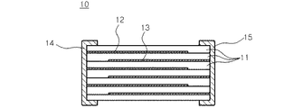
図1は本発明の一実施形態による積層セラミックスコンデンサの断面図であり、図2aは本発明の一実施形態によるセラミックスグリーンシートの断面図であり、図2bは本発明の比較例によるセラミックスグリーンシートの断面図であり、図3aから図3cは本発明の一実施形態によるセラミックスグリーンシートの製造方法を示す工程図であり、図4は本発明の他の実施形態によるセラミックスグリーンシートの断面図であり、図5は本発明の一実施形態によるセラミックスグリーンシートの端部を示す写真である。 1 is a cross-sectional view of a multilayer ceramic capacitor according to an embodiment of the present invention, FIG. 2a is a cross-sectional view of a ceramic green sheet according to an embodiment of the present invention, and FIG. 2b is a ceramic green sheet according to a comparative example of the present invention. 3a to 3c are process diagrams illustrating a method for manufacturing a ceramic green sheet according to an embodiment of the present invention, and FIG. 4 is a cross-sectional view of a ceramic green sheet according to another embodiment of the present invention. FIG. 5 is a photograph showing an end of a ceramic green sheet according to an embodiment of the present invention.
図1は本発明の一実施形態による積層セラミックスコンデンサの断面図である。 FIG. 1 is a cross-sectional view of a multilayer ceramic capacitor according to an embodiment of the present invention.
図1を参照すると、本発明の一実施形態による積層セラミックスコンデンサ10は、複数の誘電体シート11が積層されて積層体を形成し、上記積層体の外部に相異なる極性を有する外部電極14、15が形成され、上記積層体の内部に交互に積層された内部電極12、13が夫々上記外部電極に連結されることができる。
Referring to FIG. 1, a multilayer
上記誘電体シートの間に交互に形成された内部電極12、13が、夫々相異なる極性を有するように連結されて容量結合を起こすことにより、上記積層セラミックスコンデンサがキャパシタンス値を有するようになる。
The
積層セラミックスコンデンサ10を製造するためには、基材に比べて表面エネルギーが低いコーティング層を基材上に形成し、上記コーティング層を覆うように、上記コーティング層よりも表面エネルギーが高いセラミックスグリーンシートを形成する。上記セラミックスグリーンシートは、誘電体シート11として後に焼成などの過程を経ることができる。セラミックスグリーンシート上には導電性物質を塗布して、内部電極を印刷することができる。上記セラミックスグリーンシート、コーティング層及び基材を含むように切断ラインを形成し、上記切断ラインに沿って基材、コーティング層及びセラミックスグリーンシートを切断する。
In order to manufacture the multilayer
その後、基材から切断されたセラミックスグリーンシートを分離及び積層して積層本体を形成し、上記積層本体の両端に外部電極14、15を夫々の内部電極12、13に連結されるように形成することにより、積層セラミックスコンデンサ10が製造される。
Thereafter, the ceramic green sheets cut from the base material are separated and laminated to form a laminated body, and
セラミックスグリーンシートを製造するにあたり、まず、基材上にスラリーを塗布してセラミックスグリーンシートを形成し、その上に内部電極などを形成した後、基材からセラミックスグリーンシートを分離及び積層して、積層本体を形成することができる。 In producing a ceramic green sheet, first, a slurry is applied on a base material to form a ceramic green sheet, an internal electrode and the like are formed thereon, and then the ceramic green sheet is separated and laminated from the base material. A laminated body can be formed.
セラミックスグリーンシートと基材の間にはコーティング層が形成されるが、上記コーティング層はセラミックスグリーンシートに比べて表面エネルギーが小さい物質からなり、後にセラミックスグリーンシートの分離を容易にする。 A coating layer is formed between the ceramic green sheet and the substrate. The coating layer is made of a material having a surface energy smaller than that of the ceramic green sheet and facilitates separation of the ceramic green sheet later.
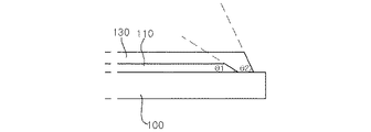
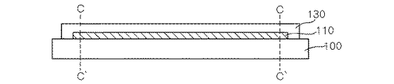
図2aは基材100上にセラミックスグリーンシート130を形成したものを図示した図面である。基材100上にコーティング層110が形成され、上記コーティング層110上にセラミックスグリーンシート130が形成されることができる。
FIG. 2 a is a diagram illustrating a ceramic
ここで、コーティング層110は、セラミックスグリーンシート130の分離を容易にするため、セラミックスグリーンシート130よりも表面エネルギーが小さい物質を用いる。
Here, the
基材100は、28mN/m以上の表面エネルギーを有する物質であり、これに制限されるものではないが、ポリエチレンテレフタレート(polyethylene terephthalate)、ポリプロピレン(polypropylnene)、ポリエチレン(polyethylene)などを含むことができる。上記基材100は、スラリー形態のセラミックスグリーンシートを塗布及び乾燥するキャリアフィルム(carrier film)として用いられる。
The
一方、コーティング層は一例としてシリコーン(Si)を含むことができ、シリコーンを含むコーティング層の場合、22mN/m以下の表面エネルギーを有することができる。 On the other hand, the coating layer may include silicone (Si) as an example, and the coating layer including silicone may have a surface energy of 22 mN / m or less.
セラミックスグリーンシート130の場合、22〜28mN/mの表面エネルギーを有するため、基材100に比べて表面エネルギーが小さいが、シリコーンコーティング層110に比べて表面エネルギーが大きくなる。セラミックスグリーンシートと基材とコーティング層との間の表面エネルギーは、次のような式を満足する。
In the case of the ceramic
εコーティング層≦εセラミックスグリーンシート≦ε基材 ε coating layer ≦ ε ceramic green sheet ≦ ε substrate
従って、コーティング層110の端部で、基材100とコーティング層110が接触する接触角θ1は90゜未満の値を有するが、これは基材100の表面エネルギーがより大きいからである。
Therefore, the contact angle θ 1 at which the
一方、セラミックスグリーンシート130がコーティング層110を覆うように形成された場合、セラミックスグリーンシート130の端部で、基材100とセラミックスグリーンシート130が接触する接触角θ2も90゜未満の値を有するが、これは基材100の表面エネルギーがより大きいからである。
On the other hand, when the ceramic
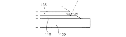
しかし、本発明の比較例である図2bの場合、セラミックスグリーンシート135とコーティング層110が接触する場合、接触角θ3は90゜以上の値を有するが、これはセラミックスグリーンシート135の表面エネルギーがより大きいからである。従って、セラミックスグリーンシート135は後の工程で剥離されやすくなる。
However, in the case of FIG. 2 b which is a comparative example of the present invention, when the ceramic
従って、本発明の一実施形態による図2aを参照すると、セラミックスグリーンシート130は基材100と接触して90゜未満の接触角を有するように形成されるため、セラミックスグリーンシート130が剥離される現象を防止することができる。
Accordingly, referring to FIG. 2a according to an embodiment of the present invention, the ceramic
また、2μm以下の薄膜セラミックスグリーンシートを製造するにあたり、非常に短い乾燥時間内にセラミックスグリーンシートのスラリー内部に含まれた誘電体パウダーの再配列を容易にするために、スラリーの固形分との粘度を落とさなければならないが、ここでスラリーの固形分との粘度が減少するにつれてスラリーの乾燥収縮率が増加する。 Further, in manufacturing a thin film ceramic green sheet of 2 μm or less, in order to facilitate rearrangement of the dielectric powder contained in the ceramic green sheet slurry within a very short drying time, The viscosity must be reduced, where the drying shrinkage of the slurry increases as the viscosity with the solids of the slurry decreases.
しかし、本発明の一実施形態によると、セラミックスグリーンシート130の端部で基材100と接するようになり、基材100の表面エネルギーはセラミックスグリーンシート130の表面エネルギーよりも大きいため、セラミックスグリーンシート130が基材100から剥離されることを防止することができる。
However, according to one embodiment of the present invention, the ceramic
図3aから図3cは本発明の一実施形態によるセラミックスグリーンシートの製造方法を示す工程図である。 3a to 3c are process diagrams illustrating a method for manufacturing a ceramic green sheet according to an embodiment of the present invention.
本発明の一実施形態によるセラミックスグリーンシートの製造方法は、基材上に基材に比べて表面エネルギーが低いコーティング層を形成する段階、及びコーティング層を覆うように、上記コーティング層よりも表面エネルギーが高いセラミックスグリーンシートを形成する段階を含む。 A method for producing a ceramic green sheet according to an embodiment of the present invention includes a step of forming a coating layer having a lower surface energy than the substrate on the substrate, and a surface energy higher than that of the coating layer so as to cover the coating layer. Forming a high ceramic green sheet.
図3aを参照すると、セラミックスグリーンシートを製造するために、基材100を準備する。上記基材は、ポリエチレンテレフタレート(polyethylene terephthalate)、ポリプロピレン(polypropylnene)、またはポリエチレン(polyethylene)を含む物質からなることができる。
Referring to FIG. 3a, a
図3bを参照すると、基材100上に基材に比べて表面エネルギーが低いコーティング層を形成する。基材100上に基材に比べて表面エネルギーが低い物質をコーティングすることによりセラミックスグリーンシートスラリーを製造し、コーティング層上にセラミックスグリーンシートを形成した後、切断及び分離段階で基材からセラミックスグリーンシートが容易に分離されるようにする。
Referring to FIG. 3b, a coating layer having a lower surface energy than that of the substrate is formed on the
ポリエチレンテレフタレートフィルムのような基材100の場合、28mN/m以上の表面エネルギーを有する。一方、コーティング層は一例としてシリコーン(Si)を含むことができ、シリコーンを含むコーティング層の場合、22mN/m以下の表面エネルギーを有することができる。
In the case of the
コーティング層110の場合、基材100に比べて表面エネルギーが小さいため、コーティング層110が基材100に密着される。
In the case of the
図3cを参照すると、基材100上にコーティング層110を形成した後、コーティング層110を覆うように、セラミックスグリーンシートスラリーを塗布して、セラミックスグリーンシート130を形成することができる。
Referring to FIG. 3 c, after forming the
セラミックスグリーンシートスラリーは、セラミックスパウダー、バインダ(binder)及び溶剤を混合して形成される。 The ceramic green sheet slurry is formed by mixing ceramic powder, a binder, and a solvent.
上記セラミックスパウダーは、これに制限されるものではないが、チタン酸バリウムのような微細粉末を用いることができ、バインダとしてはこれに制限されるものではないが、セラミックスグリーンシートが積層された時の密着性の向上及び脱バインダ効果のために、水溶性アクリル系ポリマー、ポリビニールアルコール(polyvinyl alcohol)、メチルセルロース(methyl cellulose)などが用いられることができる。 The ceramic powder is not limited to this, but a fine powder such as barium titanate can be used, and the binder is not limited to this, but when the ceramic green sheets are laminated Water-soluble acrylic polymer, polyvinyl alcohol, methyl cellulose, and the like can be used for improving the adhesion and removing the binder.
そして、上記スラリーは、ロールコータ(roll cotter)のような方式によって基材100上に塗布されることができる。その後、基材100上に塗布されたスラリーは、乾燥されてセラミックスグリーンシートを形成する。
The slurry may be applied on the
一方、セラミックスグリーンシート130の場合、22〜28mN/mの表面エネルギーを有するため、基材100に比べて表面エネルギーが小さいが、シリコーンコーティング層110に比べて表面エネルギーが大きい。
On the other hand, since the ceramic
従って、コーティング層110に対しては容易に剥離されるが、基材100に対しては密着されるようになる。
Therefore, it is easily peeled off from the
その後、セラミックスグリーンシート130の上下に、基材100、コーティング層110及びセラミックスグリーンシート130を含む切断ラインC−C’を形成し、上記切断ラインC−C’に沿って切断して、セラミックスグリーンシート130を基材100から分離することにより、図1の誘電体シート11を製造することができる。
Thereafter, a cutting line CC ′ including the
ここで、切断されたセラミックスグリーンシート130の場合、セラミックスグリーンシート130の下面に形成されたコーティング層110に比べて表面エネルギーが大きいため、容易に剥離される。
Here, since the cut ceramic
本発明の一実施形態によると、セラミックスグリーンシート130の端部が切断される前は、セラミックスグリーンシート130よりも表面エネルギーが大きい基材100に付着されていることにより、基材100から剥離されにくく、セラミックスグリーンシート130が基材100から剥離されたり、端部に波形欠陥が発生することを防止することができる。これにより、工程中に剥離されたセラミックスグリーンシート130が異物としてセラミックスグリーンシート130の表面にピンホールを形成するなどの不良を防止することができる。
According to one embodiment of the present invention, before the end of the ceramic
また、セラミックスグリーンシート130は、切断された後にその端部がセラミックスグリーンシート130よりも表面エネルギーが小さいコーティング層110に接するように形成されるため、基材100から容易に分離されることができる。
In addition, since the ceramic
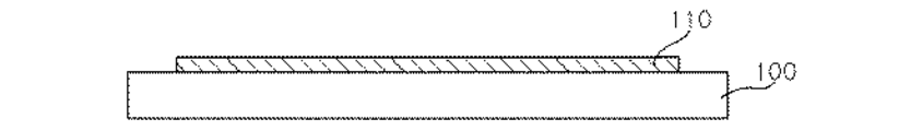
図4は本発明の他の実施形態によるセラミックスグリーンシートの断面図である。 FIG. 4 is a cross-sectional view of a ceramic green sheet according to another embodiment of the present invention.
積層セラミックスコンデンサを製造するために、上記セラミックスグリーンシート130を切断し、基材100からセラミックスグリーンシート130を分離及び積層して積層本体を形成することができる。
In order to manufacture a multilayer ceramic capacitor, the ceramic
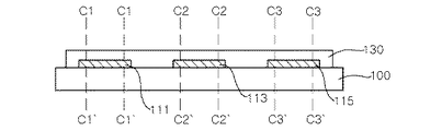
本発明の一実施形態によると、上記セラミックスグリーンシート130を切断するために切断ラインを形成することができる。切断ライン上にセラミックスグリーンシート130、コーティング層111、113、115及び基材100が位置するように切断ラインを形成し、上記切断ラインに沿ってセラミックスグリーンシートを切断することができる。
According to an embodiment of the present invention, a cutting line may be formed to cut the ceramic
図4を参照すると、切断ラインC1−C1'上にセラミックスグリーンシート130、第1コーティング層111及び基材100が位置するように切断ラインC1−C1'を形成し、切断ラインC2−C2'上にセラミックスグリーンシート130、第1コーティング層113及び基材100が位置するように切断ラインC2−C2'を形成し、切断ラインC3−C3'上にセラミックスグリーンシート130、第1コーティング層115及び基材100が位置するように切断ラインC3−C3'を形成することができる。
Referring to FIG. 4, the cutting line C1-C1 ′ is formed on the cutting line C1-C1 ′ so that the ceramic
本発明の一実施形態による図3cを参照すると、基材100上にコーティング層110を形成し、上記コーティング層110上にセラミックスグリーンシート130を形成して、切断ラインC−C’を形成することができる。
Referring to FIG. 3 c according to an embodiment of the present invention, a
そして、本発明の他の実施形態による図4を参照すると、基材100上の必要な部分にのみコーティング層111、113、115を部分的に形成した後、上記コーティング層111、113、115を覆うようにセラミックスグリーンシート130を形成する。そして、基材100、コーティング層111、113、115及びセラミックスグリーンシート130を含むように切断ラインC1−C1'、C2−C2'、C3−C3'を形成することができる。
Referring to FIG. 4 according to another embodiment of the present invention, the coating layers 111, 113, 115 are partially formed only on necessary portions on the
即ち、コーティング層を基材100全てに塗布する必要がなく、部分的に必要な部分にのみ塗布するため、コーティング層で消耗される材料を減少させ、セラミックスグリーンシート130と基材100との間の接触強度が高くなる地点を多く確保することにより、印刷工程中にセラミックスグリーンシート130が基材100から浮き上がったり、または剥離される現象を防止することができる。
That is, since it is not necessary to apply the coating layer to the
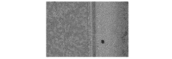
図5は本発明の一実施形態によるセラミックスグリーンシートの端部を示す写真である。 FIG. 5 is a photograph showing an end of a ceramic green sheet according to an embodiment of the present invention.
従来は、基材の全体面積に亘ってコーティング層が形成され、これによってセラミックスグリーンシートはコーティング層上にのみ存在していた。これにより、セラミックスグリーンシートよりも表面エネルギーが低いコーティング層上にセラミックスグリーンシートが位置するため、セラミックスグリーンシートが浮き上がったり、剥離されて波形欠陥などの様々な不良が発生した。 In the past, a coating layer was formed over the entire area of the substrate, whereby the ceramic green sheet was present only on the coating layer. As a result, since the ceramic green sheet is positioned on the coating layer having a lower surface energy than the ceramic green sheet, the ceramic green sheet is lifted or peeled off, and various defects such as a waveform defect are generated.
しかし、本発明の一実施形態によると、セラミックスグリーンシートの端部は相対的に表面エネルギーが高い基材と接しているため、セラミックスグリーンシートの基材に対する接着強度が高くなり、内部電極の印刷工程などでセラミックスグリーンシートが基材から剥離される現象を防止することができる。 However, according to one embodiment of the present invention, since the end portion of the ceramic green sheet is in contact with the substrate having a relatively high surface energy, the adhesive strength of the ceramic green sheet to the substrate is increased, and the printing of the internal electrode is performed. It is possible to prevent a phenomenon that the ceramic green sheet is peeled off from the substrate in a process or the like.
また、切断及び剥離工程において、セラミックスグリーンシート、コーティング層及び基材が境界面に位置するように切断ラインを形成して切断することにより、切断後にはコーティング層とセラミックスグリーンシートが境界面をなすため、相対的に表面エネルギーが低いコーティング層に付着されたセラミックスグリーンシートが容易に剥離されることができる。 In the cutting and peeling process, the cutting layer is formed so that the ceramic green sheet, the coating layer, and the base material are located on the boundary surface, and the coating layer and the ceramic green sheet form the boundary surface after cutting. Therefore, the ceramic green sheet attached to the coating layer having a relatively low surface energy can be easily peeled off.
図5を参照すると、左側部分が基材を示し、右側部分がセラミックスグリーンシートを示す。基材とセラミックスグリーンシートの境界面をみると線形に塗布されたことが分かる。即ち、波形欠陥が発生せず、一直線を形成するように塗布されたことが分かる。 Referring to FIG. 5, the left side portion shows the base material, and the right side portion shows the ceramic green sheet. When the interface between the base material and the ceramic green sheet is seen, it can be seen that it was applied linearly. That is, it can be seen that the coating was formed so as to form a straight line without generating a waveform defect.
これにより、後の工程でセラミックスグリーンシートが浮き上がったり剥離されて、異物が発生したりピンホールが発生する不良が顕著に減少するようになり、最終的にチップの不良率が減少するようになる。 As a result, the ceramic green sheet is lifted or peeled off in a later process, and the occurrence of foreign matter or pinholes is remarkably reduced, and the defective rate of chips is finally reduced. .
本発明の一実施形態によると、セラミックスグリーンシートの波形欠陥を除去することができる。このような技術により、セラミックスグリーンシートを製造するためのスラリーの固形分及び粘度を所望通り調節することが可能になる。 According to one embodiment of the present invention, the waveform defect of the ceramic green sheet can be removed. Such a technique makes it possible to adjust the solid content and viscosity of the slurry for producing the ceramic green sheet as desired.
また、本発明の一実施形態によると、簡単な方法で波形欠陥を除去するため、後の製造工程で異物が発生したりセラミックスグリーンシート表面にピンホールが発生することを防止することができ、これにより、積層セラミックスコンデンサを製造するにあたり、製品の不良率が顕著に減少するようになる。 In addition, according to one embodiment of the present invention, in order to remove the waveform defects by a simple method, it is possible to prevent the occurrence of foreign matter in the subsequent manufacturing process or the generation of pinholes on the ceramic green sheet surface, Thereby, when manufacturing a multilayer ceramic capacitor, the defective rate of a product will fall notably.
10 積層セラミックスコンデンサ
11 複数の誘電体シート
12、13 第1及び第2内部電極
14、15 第1及び第2外部電極
100 基材
110 コーティング層
111、113、115 第1コーティング層、第2コーティング層、第3コーティング層
130、135 セラミックスグリーンシート
C−C' 切断ライン
DESCRIPTION OF
Claims (12)
前記基材上に形成され、前記基材に比べて表面エネルギーが低いコーティング層、及び、
前記コーティング層を覆うように形成され、前記コーティング層よりも表面エネルギーが高いセラミックスグリーンシート、
を含む積層セラミックス電子部品用セラミックスグリーンシート。 Base material for producing ceramic green sheets for laminated ceramic electronic parts,
A coating layer formed on the substrate and having a lower surface energy than the substrate; and
A ceramic green sheet formed so as to cover the coating layer and having a higher surface energy than the coating layer,
Ceramic green sheet for laminated ceramic electronic parts.
前記コーティング層を覆うように、前記コーティング層よりも表面エネルギーが高いセラミックスグリーンシートを形成する段階、
を含む積層セラミックス電子部品用セラミックスグリーンシートの製造方法。 Forming a coating layer on the substrate having a lower surface energy than the substrate; and
Forming a ceramic green sheet having a surface energy higher than that of the coating layer so as to cover the coating layer;
For producing a ceramic green sheet for laminated ceramic electronic parts.
前記コーティング層を覆うように、前記コーティング層よりも表面エネルギーが高いセラミックスグリーンシートを形成する段階、
セラミックスグリーンシート、コーティング層及び基材を含むようにセラミックスグリーンシートを切断する段階、及び、
基材とコーティング層から切断されたセラミックスグリーンシートを分離し、前記切断されたセラミックスグリーンシートを積層する段階、
を含む積層セラミックス電子部品の製造方法。 Forming a coating layer on the substrate having a lower surface energy than the substrate;
Forming a ceramic green sheet having a surface energy higher than that of the coating layer so as to cover the coating layer;
Cutting the ceramic green sheet to include the ceramic green sheet, the coating layer and the substrate; and
Separating the cut ceramic green sheets from the substrate and the coating layer, and laminating the cut ceramic green sheets;
For producing a multilayer ceramic electronic component comprising:
Applications Claiming Priority (2)
| Application Number | Priority Date | Filing Date | Title |
|---|---|---|---|
| KR10-2010-0114139 | 2010-11-16 | ||
| KR1020100114139A KR20120052820A (en) | 2010-11-16 | 2010-11-16 | A fabricating method for green sheet for layered ceramic device and green sheet for layered ceramic device using thereof |
Publications (1)
| Publication Number | Publication Date |
|---|---|
| JP2012106901A true JP2012106901A (en) | 2012-06-07 |
Family
ID=46269321
Family Applications (1)
| Application Number | Title | Priority Date | Filing Date |
|---|---|---|---|
| JP2011037988A Pending JP2012106901A (en) | 2010-11-16 | 2011-02-24 | Method for manufacturing ceramic green sheet for multilayer ceramic electronic component and ceramic green sheet for multilayer ceramic electronic component using the same |
Country Status (2)
| Country | Link |
|---|---|
| JP (1) | JP2012106901A (en) |
| KR (1) | KR20120052820A (en) |
Citations (2)
| Publication number | Priority date | Publication date | Assignee | Title |
|---|---|---|---|---|
| JPH0837381A (en) * | 1994-07-21 | 1996-02-06 | Hitachi Chem Co Ltd | Manufacture of multilayered wiring board with terminal |
| JP2002121075A (en) * | 2000-10-06 | 2002-04-23 | Murata Mfg Co Ltd | Method of producing ceramic green sheet and multilayer ceramic electronic component |
-
2010
- 2010-11-16 KR KR1020100114139A patent/KR20120052820A/en not_active Withdrawn
-
2011
- 2011-02-24 JP JP2011037988A patent/JP2012106901A/en active Pending
Patent Citations (2)
| Publication number | Priority date | Publication date | Assignee | Title |
|---|---|---|---|---|
| JPH0837381A (en) * | 1994-07-21 | 1996-02-06 | Hitachi Chem Co Ltd | Manufacture of multilayered wiring board with terminal |
| JP2002121075A (en) * | 2000-10-06 | 2002-04-23 | Murata Mfg Co Ltd | Method of producing ceramic green sheet and multilayer ceramic electronic component |
Also Published As
| Publication number | Publication date |
|---|---|
| KR20120052820A (en) | 2012-05-24 |
Similar Documents
| Publication | Publication Date | Title |
|---|---|---|
| CN1307668C (en) | Ceramic electronic element and mfg. method thereof | |
| TWI500056B (en) | Multilayer ceramic capacitor and mounting board for multilayer ceramic capacitor | |
| TWI453777B (en) | Laminated chip electronic component, board for mounting the same, and packing unit thereof | |
| KR101275426B1 (en) | Conductive paste composition for internal electrode, multilayer ceramic capacitor and method of manufacturing the same | |
| JP2013149939A (en) | Multilayer ceramic electronic component and fabrication method thereof | |
| JP2013149936A (en) | Multilayer ceramic electronic component and fabrication method thereof | |
| JP2011124571A (en) | Conductive paste composition for external electrode, multilayer ceramic capacitor containing the same, and method of manufacturing the same | |
| US7799409B2 (en) | Ceramic green sheet structure and method for manufacturing laminated ceramic electronic component | |
| KR20120054843A (en) | Apparatus for forming electrode and method for forming electrode using the same | |
| CN111312515B (en) | Multilayer Ceramic Electronic Assemblies | |
| JP2009124155A (en) | Method of manufacturing multi-layer ceramic condenser | |
| JP2022170666A (en) | Laminated electronic component and manufacturing method thereof | |
| JPWO2004088686A1 (en) | Manufacturing method of multilayer ceramic electronic component | |
| JP2010192787A (en) | Film capacitor | |
| JP2012106901A (en) | Method for manufacturing ceramic green sheet for multilayer ceramic electronic component and ceramic green sheet for multilayer ceramic electronic component using the same | |
| JP2012114403A (en) | Ceramic composition for multilayer ceramic capacitor, multilayer ceramic capacitor including the same, and manufacturing method for the multilayer ceramic capacitor | |
| US7338854B2 (en) | Method for manufacturing multilayer ceramic capacitor | |
| JP2012144034A (en) | Green sheet and method of manufacturing the same | |
| JP2015164797A (en) | Release film and method for manufacturing multilayer ceramic electronic component using the same | |
| US20130112338A1 (en) | Method of manufacturing multilayer ceramic capacitor | |
| JP4475425B2 (en) | Multilayer ceramic capacitor | |
| JP2003264120A (en) | Ceramic electronic component and its manufacturing method | |
| JPH1126289A (en) | Manufacture of multilayered ceramic electronic component | |
| JP2003272947A (en) | Ceramic electronic component and its manufacturing method | |
| KR20050075903A (en) | Multi layer ceramic capacitor and manufacturing process thereof |
Legal Events
| Date | Code | Title | Description |
|---|---|---|---|
| RD04 | Notification of resignation of power of attorney |
Free format text: JAPANESE INTERMEDIATE CODE: A7424 Effective date: 20131118 |
|
| A621 | Written request for application examination |
Free format text: JAPANESE INTERMEDIATE CODE: A621 Effective date: 20140128 |
|
| A977 | Report on retrieval |
Free format text: JAPANESE INTERMEDIATE CODE: A971007 Effective date: 20140717 |
|
| A131 | Notification of reasons for refusal |
Free format text: JAPANESE INTERMEDIATE CODE: A131 Effective date: 20140722 |
|
| A601 | Written request for extension of time |
Free format text: JAPANESE INTERMEDIATE CODE: A601 Effective date: 20141022 |
|
| A602 | Written permission of extension of time |
Free format text: JAPANESE INTERMEDIATE CODE: A602 Effective date: 20141027 |
|
| A521 | Written amendment |
Free format text: JAPANESE INTERMEDIATE CODE: A523 Effective date: 20141121 |
|
| A02 | Decision of refusal |
Free format text: JAPANESE INTERMEDIATE CODE: A02 Effective date: 20150512 |