JP2010141024A - 半導体装置の製造方法および半導体装置 - Google Patents
半導体装置の製造方法および半導体装置 Download PDFInfo
- Publication number
- JP2010141024A JP2010141024A JP2008314540A JP2008314540A JP2010141024A JP 2010141024 A JP2010141024 A JP 2010141024A JP 2008314540 A JP2008314540 A JP 2008314540A JP 2008314540 A JP2008314540 A JP 2008314540A JP 2010141024 A JP2010141024 A JP 2010141024A
- Authority
- JP
- Japan
- Prior art keywords
- wiring
- inter
- semiconductor device
- wirings
- insulating film
- Prior art date
- Legal status (The legal status is an assumption and is not a legal conclusion. Google has not performed a legal analysis and makes no representation as to the accuracy of the status listed.)
- Pending
Links
Images


Classifications
-
- H—ELECTRICITY
- H10—SEMICONDUCTOR DEVICES; ELECTRIC SOLID-STATE DEVICES NOT OTHERWISE PROVIDED FOR
- H10W—GENERIC PACKAGES, INTERCONNECTIONS, CONNECTORS OR OTHER CONSTRUCTIONAL DETAILS OF DEVICES COVERED BY CLASS H10
- H10W20/00—Interconnections in chips, wafers or substrates
- H10W20/01—Manufacture or treatment
- H10W20/071—Manufacture or treatment of dielectric parts thereof
- H10W20/072—Manufacture or treatment of dielectric parts thereof of dielectric parts comprising air gaps
-
- H—ELECTRICITY
- H10—SEMICONDUCTOR DEVICES; ELECTRIC SOLID-STATE DEVICES NOT OTHERWISE PROVIDED FOR
- H10W—GENERIC PACKAGES, INTERCONNECTIONS, CONNECTORS OR OTHER CONSTRUCTIONAL DETAILS OF DEVICES COVERED BY CLASS H10
- H10W20/00—Interconnections in chips, wafers or substrates
- H10W20/01—Manufacture or treatment
- H10W20/071—Manufacture or treatment of dielectric parts thereof
- H10W20/074—Manufacture or treatment of dielectric parts thereof of dielectric parts comprising thin functional dielectric layers, e.g. dielectric etch-stop, barrier, capping or liner layers
- H10W20/076—Manufacture or treatment of dielectric parts thereof of dielectric parts comprising thin functional dielectric layers, e.g. dielectric etch-stop, barrier, capping or liner layers in via holes or trenches
-
- H—ELECTRICITY
- H10—SEMICONDUCTOR DEVICES; ELECTRIC SOLID-STATE DEVICES NOT OTHERWISE PROVIDED FOR
- H10W—GENERIC PACKAGES, INTERCONNECTIONS, CONNECTORS OR OTHER CONSTRUCTIONAL DETAILS OF DEVICES COVERED BY CLASS H10
- H10W20/00—Interconnections in chips, wafers or substrates
- H10W20/40—Interconnections external to wafers or substrates, e.g. back-end-of-line [BEOL] metallisations or vias connecting to gate electrodes
- H10W20/45—Interconnections external to wafers or substrates, e.g. back-end-of-line [BEOL] metallisations or vias connecting to gate electrodes characterised by their insulating parts
- H10W20/46—Interconnections external to wafers or substrates, e.g. back-end-of-line [BEOL] metallisations or vias connecting to gate electrodes characterised by their insulating parts comprising air gaps
Landscapes
- Internal Circuitry In Semiconductor Integrated Circuit Devices (AREA)
- Formation Of Insulating Films (AREA)
Abstract
【解決手段】酸素を含有する層間絶縁膜IL1の複数の溝部の側壁を被覆するバリア金属層ALが形成される。複数の溝部を充填するように配線金属層PCが形成される。層間絶縁膜IL1の酸素を熱拡散させることによってバリア金属層ALの少なくとも一部を酸化することで、酸化物バリア層BL1が形成される。配線金属層のうち複数の溝部の外側の部分を除去することによって、第1および第2の配線間領域IW1,IW2と第1〜第3の配線WR1〜WR3とが形成される。第1の配線間領域IW1を覆い、かつ第2の配線間領域IW2上に開口部OPを有するライナー膜LN1が形成される。開口部OPを介したエッチングが行なわれる。
【選択図】図2
Description
酸素を含有する層間絶縁膜が半導体基板上に形成される。層間絶縁膜に第1〜第3の溝部が形成される。金属からなり、第1〜第3の溝部の各々の側壁を被覆するバリア金属層が形成される。第1〜第3の溝部を充填するように層間絶縁膜上に、銅を含有する配線金属層が形成される。層間絶縁膜に含有される酸素を熱拡散させることによってバリア金属層の少なくとも一部を酸化することで、金属酸化物からなる酸化物バリア層が形成される。配線金属層のうち第1〜第3の溝部の外側の部分を除去することによって、第1の配線間領域によって互いに分離された第1および第2の配線と、第2の配線間領域によって第2の配線と分離された第3の配線とが形成される。第1〜第3の配線が形成された後に、第1および第2の配線間領域と第1〜第3の配線との上に位置し、かつ第1の配線間領域を覆い、かつ第2の配線間領域上に開口部を有するライナー膜が形成される。開口部を介したエッチングにより層間絶縁膜のうち第2の配線間領域の部分を除去することによって、第2の配線間領域を気体および真空のいずれかによって満たすエアギャップ部が形成され、かつ層間絶縁膜のうち第1の配線間領域の部分が残存される。
(実施の形態1)
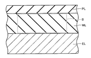
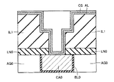
図1は、本発明の実施の形態1における半導体装置の構成を概略的に示す部分断面図である。図1を参照して、本実施の形態の半導体装置は、半導体基板ELと、多層配線層WLと、パッシベーション層PLとを有する。半導体基板ELの多層配線層WL側には、トランジスタなどの半導体素子(図示せず)が形成されている。多層配線層WLは半導体基板EL上に形成されている。パッシベーション層PLは多層配線層WL上に形成されている。
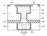
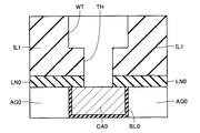
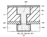
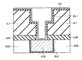
本実施の形態によれば、開口部OP(図9)を介したエッチングにより上部層間絶縁膜IL1のうち第2の配線間領域IW2の部分を除去することによって、図2に示すように、第2の配線間領域IW2を気体および真空のいずれかによって満たす上部エアギャップAG1が形成され、かつ上部層間絶縁膜IL1のうち第1の配線間領域IW1の部分が残存される。これにより、第2および第3の配線WR2,WR3の間の配線間容量を低減するための上部エアギャップAG1を有し、かつ第1の配線間領域IW1に位置する上部層間絶縁膜IL1によって機械的強度が高められた半導体装置を得ることができる。
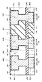
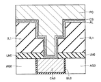
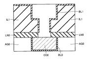
図11は、本発明の実施の形態2における半導体装置の構成を、図1の破線部IIに示す図示範囲において概略的に示す部分断面図である。また図12は、図11の破線部XIIの概略拡大図である。図11および図12を参照して、本実施の形態の半導体装置は、上部配線CA1および下部配線CA0からなる配線CA(実施の形態1)の代わりに、上部配線CC1および下部配線CC0からなる配線CCを有する。配線CCは、上部酸化アルミニウム層BL1に含まれる酸化アルミニウムに含有される金属元素であるアルミニウム元素を含有していない。より具体的には、配線CCは、たとえば純銅からなる。
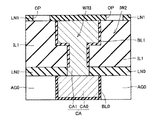
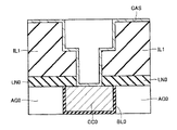
図17は、本発明の実施の形態3における半導体装置の製造方法の一工程を概略的に示す部分断面図である。図17を参照して、図4(実施の形態1)と同様に、上部層間絶縁膜IL1に溝部が形成された後、この溝部の側壁および底面を被覆する銅・アルミニウム・シード層CAS(バリア金属層)が形成される。銅・アルミニウム・シード層CASは、銅およびアルミニウムの合金からなり、たとえばPVD(Physical Vapor Deposition)法により形成することができる。この後、実施の形態1における図6(実施の形態1)の銅層PCの形成工程、およびそれ以降の工程と同様の工程が行なわれることで、本実施の形態の半導体装置が形成される。
Claims (11)
- 酸素を含有する層間絶縁膜を半導体基板上に形成する工程と、
前記層間絶縁膜に第1〜第3の溝部を形成する工程と、
金属からなり、前記第1〜第3の溝部の各々の側壁を被覆するバリア金属層を形成する工程と、
前記第1〜第3の溝部を充填するように前記層間絶縁膜上に、銅を含有する配線金属層を形成する工程と、
前記層間絶縁膜に含有される酸素を熱拡散させることによって前記バリア金属層の少なくとも一部を酸化することで、金属酸化物からなる酸化物バリア層を形成する工程と、
前記配線金属層のうち前記第1〜第3の溝部の外側の部分を除去することによって、第1の配線間領域によって互いに分離された第1および第2の配線と、第2の配線間領域によって前記第2の配線と分離された第3の配線とを形成する工程と、
前記第1〜第3の配線を形成する工程の後に、前記第1および第2の配線間領域と前記第1〜第3の配線との上に位置し、かつ前記第1の配線間領域を覆い、かつ前記第2の配線間領域上に開口部を有するライナー膜を形成する工程と、
前記開口部を介したエッチングにより前記層間絶縁膜のうち前記第2の配線間領域の部分を除去することによって、前記第2の配線間領域を気体および真空のいずれかによって満たすエアギャップ部を形成し、かつ前記層間絶縁膜のうち前記第1の配線間領域の部分を残存させる工程とを備えた、半導体装置の製造方法。 - 前記第1〜第3の配線の少なくとも1つは導体部上に形成される、請求項1に記載の半導体装置の製造方法。
- 前記金属は、アルミニウム、チタン、ルテニウムおよびタンタルの少なくともいずれかの金属を含む、請求項1または2に記載の半導体装置の製造方法。
- 前記配線金属層を形成する工程は、前記酸化物バリア層を形成する工程の前に行なわれる、請求項1〜3のいずれかに記載の半導体装置の製造方法。
- 前記バリア金属層は銅を含有する、請求項4に記載の半導体装置の製造方法。
- 前記酸化物バリア層を形成する工程は、前記配線金属層を形成する工程の前に行なわれる、請求項1〜3のいずれかに記載の半導体装置の製造方法。
- 前記酸化物バリア層を形成する工程の後まで残存した前記バリア金属層を、前記配線金属層を形成する工程の前に除去する工程をさらに備えた、請求項6に記載の半導体装置の製造方法。
- 半導体基板と、
銅を含有し、前記半導体基板上に設けられた第1〜第3の配線とを備え、
前記第1および第2の配線の間は第1の配線間領域によって分離され、前記第2および第3の配線の間は第2の配線間領域によって分離され、
金属酸化物からなり、前記第1および第2の配線間領域と、前記第1〜第3の配線との界面を隔てる酸化物バリア層と、
酸素を含有し、前記第1の配線間領域を埋めこむ層間絶縁膜と、
前記第2の配線間領域を気体および真空のいずれかによって満たすエアギャップ部とをさらに備えた、半導体装置。 - 前記第1〜第3の配線の少なくとも1つの前記半導体基板側の面に接する導体部をさらに備えた、請求項8に記載の半導体装置。
- 前記金属酸化物は、アルミニウム、チタン、ルテニウムおよびタンタルの少なくともいずれかの酸化物を含む、請求項8または9に記載の半導体装置。
- 前記第1〜第3の配線は、前記金属酸化物に含有される金属元素を含有しない、請求項8〜10のいずれかに記載の半導体装置。
Priority Applications (1)
| Application Number | Priority Date | Filing Date | Title |
|---|---|---|---|
| JP2008314540A JP2010141024A (ja) | 2008-12-10 | 2008-12-10 | 半導体装置の製造方法および半導体装置 |
Applications Claiming Priority (1)
| Application Number | Priority Date | Filing Date | Title |
|---|---|---|---|
| JP2008314540A JP2010141024A (ja) | 2008-12-10 | 2008-12-10 | 半導体装置の製造方法および半導体装置 |
Publications (2)
| Publication Number | Publication Date |
|---|---|
| JP2010141024A true JP2010141024A (ja) | 2010-06-24 |
| JP2010141024A5 JP2010141024A5 (ja) | 2012-01-19 |
Family
ID=42350917
Family Applications (1)
| Application Number | Title | Priority Date | Filing Date |
|---|---|---|---|
| JP2008314540A Pending JP2010141024A (ja) | 2008-12-10 | 2008-12-10 | 半導体装置の製造方法および半導体装置 |
Country Status (1)
| Country | Link |
|---|---|
| JP (1) | JP2010141024A (ja) |
Cited By (4)
| Publication number | Priority date | Publication date | Assignee | Title |
|---|---|---|---|---|
| US8779590B2 (en) | 2011-06-16 | 2014-07-15 | Kabushiki Kaisha Toshiba | Semiconductor device and method of producing the same |
| US8940632B2 (en) | 2013-05-20 | 2015-01-27 | Samsung Electronics Co., Ltd. | Semiconductor devices and method of fabricating the same |
| WO2015130549A3 (en) * | 2014-02-28 | 2015-11-12 | Qualcomm Incorporated | Selective conductive barrier layer formation |
| WO2016118634A1 (en) * | 2015-01-21 | 2016-07-28 | Qualcomm Incorporated | Integrated circuit devices and methods |
Citations (3)
| Publication number | Priority date | Publication date | Assignee | Title |
|---|---|---|---|---|
| US20020016058A1 (en) * | 2000-06-15 | 2002-02-07 | Bin Zhao | Microelectronic air-gap structures and methods of forming the same |
| JP2006344703A (ja) * | 2005-06-08 | 2006-12-21 | Hitachi Ltd | 半導体装置およびその製造方法 |
| JP2007048974A (ja) * | 2005-08-10 | 2007-02-22 | Toshiba Corp | 半導体装置およびその製造方法 |
-
2008
- 2008-12-10 JP JP2008314540A patent/JP2010141024A/ja active Pending
Patent Citations (3)
| Publication number | Priority date | Publication date | Assignee | Title |
|---|---|---|---|---|
| US20020016058A1 (en) * | 2000-06-15 | 2002-02-07 | Bin Zhao | Microelectronic air-gap structures and methods of forming the same |
| JP2006344703A (ja) * | 2005-06-08 | 2006-12-21 | Hitachi Ltd | 半導体装置およびその製造方法 |
| JP2007048974A (ja) * | 2005-08-10 | 2007-02-22 | Toshiba Corp | 半導体装置およびその製造方法 |
Non-Patent Citations (1)
| Title |
|---|
| T.USUI ET AL.: "Low Resistive and Highly Reliable Cu Dual-Damascene Interconnect Technology Using Self-Formed MnSixO", INTERCONNECT TECHNOLOGY CONFERENCE, 2005. PROCEEDINGS OF THE IEEE 2005 INTERNATIONAL, vol. p.188-190, JPN6013043580, 8 June 2005 (2005-06-08), ISSN: 0002622757 * |
Cited By (10)
| Publication number | Priority date | Publication date | Assignee | Title |
|---|---|---|---|---|
| US8779590B2 (en) | 2011-06-16 | 2014-07-15 | Kabushiki Kaisha Toshiba | Semiconductor device and method of producing the same |
| US8940632B2 (en) | 2013-05-20 | 2015-01-27 | Samsung Electronics Co., Ltd. | Semiconductor devices and method of fabricating the same |
| WO2015130549A3 (en) * | 2014-02-28 | 2015-11-12 | Qualcomm Incorporated | Selective conductive barrier layer formation |
| US9343357B2 (en) | 2014-02-28 | 2016-05-17 | Qualcomm Incorporated | Selective conductive barrier layer formation |
| WO2016118634A1 (en) * | 2015-01-21 | 2016-07-28 | Qualcomm Incorporated | Integrated circuit devices and methods |
| US9543248B2 (en) | 2015-01-21 | 2017-01-10 | Qualcomm Incorporated | Integrated circuit devices and methods |
| US9721891B2 (en) | 2015-01-21 | 2017-08-01 | Qualcomm Incorporated | Integrated circuit devices and methods |
| CN107210286A (zh) * | 2015-01-21 | 2017-09-26 | 高通股份有限公司 | 集成电路器件和方法 |
| JP2018507546A (ja) * | 2015-01-21 | 2018-03-15 | クゥアルコム・インコーポレイテッドQualcomm Incorporated | 集積回路デバイスおよび方法 |
| CN107210286B (zh) * | 2015-01-21 | 2020-09-11 | 高通股份有限公司 | 集成电路器件和方法 |
Similar Documents
| Publication | Publication Date | Title |
|---|---|---|
| CN102362343B (zh) | 包括非常锥形的转变贯孔的半导体装置的金属化系统 | |
| US7741228B2 (en) | Method for fabricating semiconductor device | |
| JP2009194286A (ja) | 半導体装置及びその製造方法 | |
| JP5089244B2 (ja) | 半導体装置 | |
| JPH10242271A (ja) | 半導体装置及びその製造方法 | |
| JP2006019480A (ja) | 半導体装置の製造方法 | |
| JP2012038961A (ja) | 半導体装置及び半導体装置の製造方法 | |
| JP2004311930A (ja) | 多層配線を含む半導体装置およびその製造方法 | |
| JP5193542B2 (ja) | 半導体装置の製造方法 | |
| US20100117232A1 (en) | Semiconductor device and method for manufacturing the same | |
| US20070200237A1 (en) | Semiconductor device and method of manufacturing the same | |
| JP2006005190A (ja) | 半導体装置 | |
| CN112366195B (zh) | 键合方法及键合结构 | |
| EP1610376B1 (en) | Semiconductor device | |
| JP2010141024A (ja) | 半導体装置の製造方法および半導体装置 | |
| JPH10261707A (ja) | 半導体装置の製造方法 | |
| US7737030B2 (en) | Method for manufacturing a semiconductor device, and said semiconductor device | |
| CN1862818B (zh) | 半导体器件及其制造方法 | |
| JP2006324584A (ja) | 半導体装置およびその製造方法 | |
| JP4472286B2 (ja) | 変形されたデュアルダマシン工程を利用した半導体素子の金属配線形成方法 | |
| JP5424551B2 (ja) | 半導体装置 | |
| JP2007220738A (ja) | 半導体装置の製造方法 | |
| JP2009158657A (ja) | 配線構造の製造方法および配線構造 | |
| JP2006005010A (ja) | 半導体装置及びその製造方法 | |
| JP2002280450A (ja) | 半導体装置とその製造方法 |
Legal Events
| Date | Code | Title | Description |
|---|---|---|---|
| A711 | Notification of change in applicant |
Free format text: JAPANESE INTERMEDIATE CODE: A712 Effective date: 20100602 |
|
| A521 | Request for written amendment filed |
Free format text: JAPANESE INTERMEDIATE CODE: A523 Effective date: 20111130 |
|
| A621 | Written request for application examination |
Free format text: JAPANESE INTERMEDIATE CODE: A621 Effective date: 20111130 |
|
| A977 | Report on retrieval |
Free format text: JAPANESE INTERMEDIATE CODE: A971007 Effective date: 20130829 |
|
| A131 | Notification of reasons for refusal |
Free format text: JAPANESE INTERMEDIATE CODE: A131 Effective date: 20130903 |
|
| A02 | Decision of refusal |
Free format text: JAPANESE INTERMEDIATE CODE: A02 Effective date: 20140128 |