JP2010093192A - 半導体発光素子 - Google Patents
半導体発光素子 Download PDFInfo
- Publication number
- JP2010093192A JP2010093192A JP2008264114A JP2008264114A JP2010093192A JP 2010093192 A JP2010093192 A JP 2010093192A JP 2008264114 A JP2008264114 A JP 2008264114A JP 2008264114 A JP2008264114 A JP 2008264114A JP 2010093192 A JP2010093192 A JP 2010093192A
- Authority
- JP
- Japan
- Prior art keywords
- layer
- layers
- semiconductor light
- light emitting
- well
- Prior art date
- Legal status (The legal status is an assumption and is not a legal conclusion. Google has not performed a legal analysis and makes no representation as to the accuracy of the status listed.)
- Granted
Links
- 239000004065 semiconductor Substances 0.000 title claims abstract description 55
- 230000004888 barrier function Effects 0.000 claims abstract description 77
- 239000000758 substrate Substances 0.000 claims abstract description 13
- 230000003287 optical effect Effects 0.000 abstract description 12
- 230000010287 polarization Effects 0.000 abstract description 8
- 238000005253 cladding Methods 0.000 description 16
- 238000005530 etching Methods 0.000 description 7
- 238000005424 photoluminescence Methods 0.000 description 7
- 238000010586 diagram Methods 0.000 description 6
- 230000006798 recombination Effects 0.000 description 6
- 238000005215 recombination Methods 0.000 description 6
- 239000002184 metal Substances 0.000 description 5
- 238000000034 method Methods 0.000 description 5
- KRHYYFGTRYWZRS-UHFFFAOYSA-N Fluorane Chemical compound F KRHYYFGTRYWZRS-UHFFFAOYSA-N 0.000 description 4
- 230000000694 effects Effects 0.000 description 3
- VEXZGXHMUGYJMC-UHFFFAOYSA-N Hydrochloric acid Chemical compound Cl VEXZGXHMUGYJMC-UHFFFAOYSA-N 0.000 description 2
- QAOWNCQODCNURD-UHFFFAOYSA-N Sulfuric acid Chemical compound OS(O)(=O)=O QAOWNCQODCNURD-UHFFFAOYSA-N 0.000 description 2
- 230000003321 amplification Effects 0.000 description 2
- 230000015572 biosynthetic process Effects 0.000 description 2
- 239000013078 crystal Substances 0.000 description 2
- 230000005684 electric field Effects 0.000 description 2
- 238000002474 experimental method Methods 0.000 description 2
- 238000004519 manufacturing process Methods 0.000 description 2
- 239000000203 mixture Substances 0.000 description 2
- 238000003199 nucleic acid amplification method Methods 0.000 description 2
- MHAJPDPJQMAIIY-UHFFFAOYSA-N Hydrogen peroxide Chemical compound OO MHAJPDPJQMAIIY-UHFFFAOYSA-N 0.000 description 1
- 229910004298 SiO 2 Inorganic materials 0.000 description 1
- 239000000956 alloy Substances 0.000 description 1
- 229910045601 alloy Inorganic materials 0.000 description 1
- 238000005229 chemical vapour deposition Methods 0.000 description 1
- 230000006835 compression Effects 0.000 description 1
- 238000007906 compression Methods 0.000 description 1
- 230000007850 degeneration Effects 0.000 description 1
- 238000000151 deposition Methods 0.000 description 1
- 238000009792 diffusion process Methods 0.000 description 1
- 230000009036 growth inhibition Effects 0.000 description 1
- QOSATHPSBFQAML-UHFFFAOYSA-N hydrogen peroxide;hydrate Chemical compound O.OO QOSATHPSBFQAML-UHFFFAOYSA-N 0.000 description 1
- 238000003475 lamination Methods 0.000 description 1
- 239000000463 material Substances 0.000 description 1
- 239000013307 optical fiber Substances 0.000 description 1
- 238000000206 photolithography Methods 0.000 description 1
- 238000005268 plasma chemical vapour deposition Methods 0.000 description 1
- 238000007747 plating Methods 0.000 description 1
- 238000000926 separation method Methods 0.000 description 1
- 238000007740 vapor deposition Methods 0.000 description 1
- XLYOFNOQVPJJNP-UHFFFAOYSA-N water Substances O XLYOFNOQVPJJNP-UHFFFAOYSA-N 0.000 description 1
Images


Landscapes
- Semiconductor Lasers (AREA)
Abstract
【解決手段】半導体基板11上に、複数の井戸層141と複数の障壁層142とが交互に1層ずつ積層された多重量子井戸構造からなる活性層14を備え、複数の井戸層141が圧縮歪を有し、複数の障壁層142が、伸張歪を有する伸張歪障壁層143と、無歪である少なくとも2層の無歪障壁層144と、を含み、2層の無歪障壁層144の間に井戸層141と伸張歪障壁層143とが連続して積層された対が少なくとも1つ配置される構成を有している。
【選択図】図1
Description
また、本発明の半導体発光素子は、前記井戸層の層数が5〜7層である構成を有している。この構成により、優れたフォトルミネッセンス特性を得ることができる。
これらの構成により、優れたフォトルミネッセンス特性および高い光出力を得ることができる。
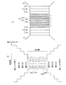
本発明に係る半導体発光素子の第1の実施形態を図1に示す。図1(a)は半導体発光素子1の構成を示す斜視図であり、図1(b)は要部の構造を示す拡大断面図である。
圧縮歪を有する井戸層141においては、重いホールバンド端141aが軽いホールバンド端141bよりもホールにとって低いエネルギー位置に存在している。一方、伸張歪障壁層143においては、軽いホールバンド端143bが重いホールバンド端143aよりもホールにとって低いエネルギー位置に存在している。なお、無歪障壁層144においては、重いホールバンドと軽いホールバンドは縮退している。
まず、有機金属気相成長(MOVPE)法を用いてn型InPからなる半導体基板11上に、n型InPからなるn型クラッド層12、これに引き続きSCH層13を成長する。なお、このSCH層は100nm程度の層厚とし、そのバンドギャップはn型クラッド層12と無歪障壁層144の間の範囲であり、かつバンドギャップ波長はSCH層13c、13b、13aの順に長くなるように配置する。
本発明に係る半導体発光素子の第2の実施形態を図3を用いて説明する。図3(a)は、半導体発光素子2の要部の構造を示す拡大断面図であり、図3(b)は、半導体発光素子2のバンド構造を模式的に示す図である。第1の実施形態と同様の構成および製造方法については説明を省略する。
14 活性層
141 井戸層
141a、143a 重いホールバンド端
141b、143b 軽いホールバンド端
142 障壁層
143 伸張歪障壁層
144 無歪障壁層
Claims (6)
- 基板上に、複数の井戸層と複数の障壁層とが交互に1層ずつ積層された多重量子井戸構造からなる活性層を備える半導体発光素子において、
前記複数の井戸層が圧縮歪を有し、
前記複数の障壁層が、伸張歪障壁層と、少なくとも2層の無歪障壁層と、を含み、
2層の前記無歪障壁層の間に前記井戸層と前記伸張歪障壁層とが連続して積層された対が少なくとも1つ配置されることを特徴とする半導体発光素子。 - 前記活性層がGaInAsPからなる請求項1に記載の半導体発光素子。
- 前記井戸層の層数が5〜7層である請求項2に記載の半導体発光素子。
- 前記井戸層の層数が6層であり、前記無歪障壁層の層数が4層であり、前記伸張歪障壁層の層数が3層である請求項3に記載の半導体発光素子。
- 前記井戸層の層数が6層であり、前記無歪障壁層の層数が3層であり、前記伸張歪障壁層の層数が4層である請求項3に記載の半導体発光素子。
- 前記基板がInPでなり、
前記伸張歪障壁層のバンドギャップ波長が0.95〜1.2μmであり、
前記無歪障壁層のバンドギャップ波長が0.95〜1.2μmであることを特徴とする請求項1から請求項5のいずれか一項に記載の半導体発光素子。
Priority Applications (1)
| Application Number | Priority Date | Filing Date | Title |
|---|---|---|---|
| JP2008264114A JP5271027B2 (ja) | 2008-10-10 | 2008-10-10 | 半導体発光素子 |
Applications Claiming Priority (1)
| Application Number | Priority Date | Filing Date | Title |
|---|---|---|---|
| JP2008264114A JP5271027B2 (ja) | 2008-10-10 | 2008-10-10 | 半導体発光素子 |
Publications (2)
| Publication Number | Publication Date |
|---|---|
| JP2010093192A true JP2010093192A (ja) | 2010-04-22 |
| JP5271027B2 JP5271027B2 (ja) | 2013-08-21 |
Family
ID=42255616
Family Applications (1)
| Application Number | Title | Priority Date | Filing Date |
|---|---|---|---|
| JP2008264114A Active JP5271027B2 (ja) | 2008-10-10 | 2008-10-10 | 半導体発光素子 |
Country Status (1)
| Country | Link |
|---|---|
| JP (1) | JP5271027B2 (ja) |
Cited By (1)
| Publication number | Priority date | Publication date | Assignee | Title |
|---|---|---|---|---|
| WO2012127882A1 (ja) | 2011-03-24 | 2012-09-27 | 株式会社メニコン | コンタクトレンズおよびその製造方法 |
Citations (6)
| Publication number | Priority date | Publication date | Assignee | Title |
|---|---|---|---|---|
| JPH0541564A (ja) * | 1991-08-06 | 1993-02-19 | Nec Corp | 半導体多重歪量子井戸構造 |
| JPH0738206A (ja) * | 1993-07-23 | 1995-02-07 | Matsushita Electric Ind Co Ltd | 歪多重量子井戸構造体およびそれを用いた半導体レーザ |
| JPH07235730A (ja) * | 1994-02-22 | 1995-09-05 | Matsushita Electric Ind Co Ltd | 歪多重量子井戸構造およびその製造方法ならびに半導体レーザ |
| JPH0832176A (ja) * | 1994-07-18 | 1996-02-02 | Sony Corp | 化合物半導体多重歪量子井戸構造 |
| JPH0878786A (ja) * | 1994-09-02 | 1996-03-22 | Mitsubishi Electric Corp | 歪量子井戸の構造 |
| JP2007201040A (ja) * | 2006-01-25 | 2007-08-09 | Anritsu Corp | 半導体発光素子 |
-
2008
- 2008-10-10 JP JP2008264114A patent/JP5271027B2/ja active Active
Patent Citations (6)
| Publication number | Priority date | Publication date | Assignee | Title |
|---|---|---|---|---|
| JPH0541564A (ja) * | 1991-08-06 | 1993-02-19 | Nec Corp | 半導体多重歪量子井戸構造 |
| JPH0738206A (ja) * | 1993-07-23 | 1995-02-07 | Matsushita Electric Ind Co Ltd | 歪多重量子井戸構造体およびそれを用いた半導体レーザ |
| JPH07235730A (ja) * | 1994-02-22 | 1995-09-05 | Matsushita Electric Ind Co Ltd | 歪多重量子井戸構造およびその製造方法ならびに半導体レーザ |
| JPH0832176A (ja) * | 1994-07-18 | 1996-02-02 | Sony Corp | 化合物半導体多重歪量子井戸構造 |
| JPH0878786A (ja) * | 1994-09-02 | 1996-03-22 | Mitsubishi Electric Corp | 歪量子井戸の構造 |
| JP2007201040A (ja) * | 2006-01-25 | 2007-08-09 | Anritsu Corp | 半導体発光素子 |
Cited By (1)
| Publication number | Priority date | Publication date | Assignee | Title |
|---|---|---|---|---|
| WO2012127882A1 (ja) | 2011-03-24 | 2012-09-27 | 株式会社メニコン | コンタクトレンズおよびその製造方法 |
Also Published As
| Publication number | Publication date |
|---|---|
| JP5271027B2 (ja) | 2013-08-21 |
Similar Documents
| Publication | Publication Date | Title |
|---|---|---|
| US8605769B2 (en) | Semiconductor laser device and manufacturing method thereof | |
| US20100142578A1 (en) | Surface-emitting laser including two-dimensional photonic crystal | |
| JP5314435B2 (ja) | 集積光デバイス及びその製造方法 | |
| US8610105B2 (en) | Semiconductor electroluminescent device with a multiple-quantum well layer formed therein | |
| JP4554526B2 (ja) | 半導体発光素子 | |
| JP4998238B2 (ja) | 集積型半導体光素子 | |
| JP5271027B2 (ja) | 半導体発光素子 | |
| JPWO2006109418A1 (ja) | 半導体発光素子 | |
| JP2004055864A (ja) | 半導体素子用基板の製造方法および半導体素子用基板ならびに半導体素子 | |
| JP5205901B2 (ja) | 半導体レーザ素子の作製方法および半導体レーザ素子 | |
| JP2010129763A (ja) | 半導体レーザおよびその製造方法 | |
| US20070160105A1 (en) | Distributed feedback laser diode and a method for manufacturing the same | |
| JP2008091420A (ja) | 量子ドット光半導体素子の製造方法 | |
| KR20150089551A (ko) | Dbr층 패턴을 포함하는 발광다이오드 및 이의 제조방법 | |
| JP2010118454A (ja) | 半導体レーザ | |
| JP5075318B2 (ja) | 窒化物半導体基板、半導体デバイス、半導体発光素子、半導体受光素子および窒化物半導体基板の製造方法 | |
| CN117296218A (zh) | 光子晶体半导体激光装置及其制造方法 | |
| JP7168138B1 (ja) | 半導体レーザ素子および半導体レーザ素子の製造方法 | |
| JP6240738B2 (ja) | 半導体光増幅器 | |
| JP6062847B2 (ja) | 半導体光増幅器 | |
| JP4671702B2 (ja) | Iii族窒化物半導体レーザ装置 | |
| JP2005260109A (ja) | 光半導体素子 | |
| JP5494464B2 (ja) | 半導体素子及び半導体素子の製造方法 | |
| JPH09232666A (ja) | 半導体レーザ及び並列伝送用光送信モジュール | |
| JP5822458B2 (ja) | 半導体レーザ素子 |
Legal Events
| Date | Code | Title | Description |
|---|---|---|---|
| A621 | Written request for application examination |
Free format text: JAPANESE INTERMEDIATE CODE: A621 Effective date: 20110831 |
|
| A977 | Report on retrieval |
Free format text: JAPANESE INTERMEDIATE CODE: A971007 Effective date: 20121010 |
|
| A131 | Notification of reasons for refusal |
Free format text: JAPANESE INTERMEDIATE CODE: A131 Effective date: 20121023 |
|
| A521 | Request for written amendment filed |
Free format text: JAPANESE INTERMEDIATE CODE: A523 Effective date: 20121207 |
|
| TRDD | Decision of grant or rejection written | ||
| A01 | Written decision to grant a patent or to grant a registration (utility model) |
Free format text: JAPANESE INTERMEDIATE CODE: A01 Effective date: 20130423 |
|
| A61 | First payment of annual fees (during grant procedure) |
Free format text: JAPANESE INTERMEDIATE CODE: A61 Effective date: 20130510 |
|
| R150 | Certificate of patent or registration of utility model |
Free format text: JAPANESE INTERMEDIATE CODE: R150 Ref document number: 5271027 Country of ref document: JP Free format text: JAPANESE INTERMEDIATE CODE: R150 |
|
| R250 | Receipt of annual fees |
Free format text: JAPANESE INTERMEDIATE CODE: R250 |
|
| R250 | Receipt of annual fees |
Free format text: JAPANESE INTERMEDIATE CODE: R250 |
|
| R250 | Receipt of annual fees |
Free format text: JAPANESE INTERMEDIATE CODE: R250 |
|
| R250 | Receipt of annual fees |
Free format text: JAPANESE INTERMEDIATE CODE: R250 |
|
| R250 | Receipt of annual fees |
Free format text: JAPANESE INTERMEDIATE CODE: R250 |
|
| R250 | Receipt of annual fees |
Free format text: JAPANESE INTERMEDIATE CODE: R250 |
|
| R250 | Receipt of annual fees |
Free format text: JAPANESE INTERMEDIATE CODE: R250 |
|
| R250 | Receipt of annual fees |
Free format text: JAPANESE INTERMEDIATE CODE: R250 |
|
| R250 | Receipt of annual fees |
Free format text: JAPANESE INTERMEDIATE CODE: R250 |
|
| R250 | Receipt of annual fees |
Free format text: JAPANESE INTERMEDIATE CODE: R250 |