JP2010068313A - コプレーナ線路及びその製造方法 - Google Patents
コプレーナ線路及びその製造方法 Download PDFInfo
- Publication number
- JP2010068313A JP2010068313A JP2008233399A JP2008233399A JP2010068313A JP 2010068313 A JP2010068313 A JP 2010068313A JP 2008233399 A JP2008233399 A JP 2008233399A JP 2008233399 A JP2008233399 A JP 2008233399A JP 2010068313 A JP2010068313 A JP 2010068313A
- Authority
- JP
- Japan
- Prior art keywords
- substrate
- signal line
- insulating film
- film
- ground conductor
- Prior art date
- Legal status (The legal status is an assumption and is not a legal conclusion. Google has not performed a legal analysis and makes no representation as to the accuracy of the status listed.)
- Granted
Links
Images


Classifications
-
- G—PHYSICS
- G02—OPTICS
- G02B—OPTICAL ELEMENTS, SYSTEMS OR APPARATUS
- G02B6/00—Light guides; Structural details of arrangements comprising light guides and other optical elements, e.g. couplings
- G02B6/10—Light guides; Structural details of arrangements comprising light guides and other optical elements, e.g. couplings of the optical waveguide type
- G02B6/12—Light guides; Structural details of arrangements comprising light guides and other optical elements, e.g. couplings of the optical waveguide type of the integrated circuit kind
- G02B6/13—Integrated optical circuits characterised by the manufacturing method
- G02B6/136—Integrated optical circuits characterised by the manufacturing method by etching
-
- H10W44/20—
-
- G—PHYSICS
- G02—OPTICS
- G02B—OPTICAL ELEMENTS, SYSTEMS OR APPARATUS
- G02B6/00—Light guides; Structural details of arrangements comprising light guides and other optical elements, e.g. couplings
- G02B6/10—Light guides; Structural details of arrangements comprising light guides and other optical elements, e.g. couplings of the optical waveguide type
- G02B6/12—Light guides; Structural details of arrangements comprising light guides and other optical elements, e.g. couplings of the optical waveguide type of the integrated circuit kind
- G02B2006/12035—Materials
- G02B2006/12061—Silicon
-
- G—PHYSICS
- G02—OPTICS
- G02B—OPTICAL ELEMENTS, SYSTEMS OR APPARATUS
- G02B6/00—Light guides; Structural details of arrangements comprising light guides and other optical elements, e.g. couplings
- G02B6/10—Light guides; Structural details of arrangements comprising light guides and other optical elements, e.g. couplings of the optical waveguide type
- G02B6/12—Light guides; Structural details of arrangements comprising light guides and other optical elements, e.g. couplings of the optical waveguide type of the integrated circuit kind
- G02B2006/12083—Constructional arrangements
- G02B2006/12097—Ridge, rib or the like
-
- G—PHYSICS
- G02—OPTICS
- G02F—OPTICAL DEVICES OR ARRANGEMENTS FOR THE CONTROL OF LIGHT BY MODIFICATION OF THE OPTICAL PROPERTIES OF THE MEDIA OF THE ELEMENTS INVOLVED THEREIN; NON-LINEAR OPTICS; FREQUENCY-CHANGING OF LIGHT; OPTICAL LOGIC ELEMENTS; OPTICAL ANALOGUE/DIGITAL CONVERTERS
- G02F2201/00—Constructional arrangements not provided for in groups G02F1/00 - G02F7/00
- G02F2201/06—Constructional arrangements not provided for in groups G02F1/00 - G02F7/00 integrated waveguide
-
- G—PHYSICS
- G02—OPTICS
- G02F—OPTICAL DEVICES OR ARRANGEMENTS FOR THE CONTROL OF LIGHT BY MODIFICATION OF THE OPTICAL PROPERTIES OF THE MEDIA OF THE ELEMENTS INVOLVED THEREIN; NON-LINEAR OPTICS; FREQUENCY-CHANGING OF LIGHT; OPTICAL LOGIC ELEMENTS; OPTICAL ANALOGUE/DIGITAL CONVERTERS
- G02F2202/00—Materials and properties
- G02F2202/10—Materials and properties semiconductor
-
- H10W44/216—
Landscapes
- Physics & Mathematics (AREA)
- Engineering & Computer Science (AREA)
- Microelectronics & Electronic Packaging (AREA)
- General Physics & Mathematics (AREA)
- Optics & Photonics (AREA)
- Waveguides (AREA)
- Structure Of Printed Boards (AREA)
Abstract
【解決手段】基板20と、基板上に形成された信号線路42と、基板上の、信号線路を挟む位置に形成された1対の接地導体44と、基板と信号線路の間に設けられた信号線路用絶縁膜32と、基板と接地導体の間に、信号線路用絶縁膜と離間して設けられた接地導体用絶縁膜34とを有して構成される。
【選択図】図1
Description
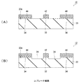
図1(A)及び(B)を参照して、この発明のコプレーナ線路について説明する。
こともある。)が用いられる。ここでは、高抵抗シリコン基板の抵抗率は、1kΩ・cm以上10kΩ・cm以下とする。
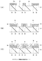
図3(A)〜(E)を参照して、コプレーナ線路の製造方法について説明する。図3(A)〜(E)は、コプレーナ線路の製造方法を説明するための工程図である。
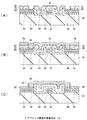
図4及び図5を参照して、エアブリッジ構造の製造方法について説明する。図4及び5は、エアブリッジ構造の製造方法を説明するための工程図である。
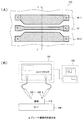
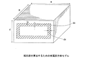
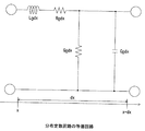
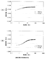
図6(A)及び(B)を参照して、コプレーナ線路の動作の評価方法を説明する。図6(A)は、図1(A)を参照して説明した一構成例のコプレーナ線路の概略的な上面図である。なお、図6(A)中、構成要素にハッチングを施してあるが、このハッチングは断面を表示するのではなく、各構成要素の領域を強調して示してあるに過ぎない。図1(A)は、図6(A)のI−I´線に沿って取った断面図に相当する。
20、22 基板
24 凹部
30 絶縁膜
32 信号線路用絶縁膜
34 接地導体用絶縁膜
40 金属膜
42 信号線路
44 接地導体
50 保護膜
52、76 開口部
62 カレントフィルム
64 金属
70、75、78 レジストパターン
124 ネットワークアナライザ
126 パーソナルコンピュータ
128 基板搭載ステージ
131−1、131−2 プローブヘッド
Claims (16)
- 基板と、
該基板上に形成された信号線路と、
前記基板上の、前記信号線路を挟む位置に形成された1対の接地導体と、
前記基板と前記信号線路の間に設けられた信号線路用絶縁膜と、
前記基板と前記接地導体の間に、前記信号線路用絶縁膜と離間して設けられた接地導体用絶縁膜と
を有することを特徴とするコプレーナ線路。 - 前記信号線路用絶縁膜及び前記接地導体用絶縁膜の厚みが200nm〜2μmである
ことを特徴とする請求項1に記載のコプレーナ線路。 - 前記信号線路用絶縁膜及び前記接地導体用絶縁膜が、シリコン酸化膜、シリコン窒化膜及びシリコン酸窒化膜のいずれか1つである
ことを特徴とする請求項1又は2に記載のコプレーナ線路。 - 前記信号線路用絶縁膜及び前記接地導体用絶縁膜が、シリコン酸化膜及びシリコン酸窒化膜のいずれか一方と、シリコン窒化膜との積層構造である
ことを特徴とする請求項1又は2に記載のコプレーナ線路。 - 前記基板が高抵抗シリコン基板である
ことを特徴とする請求項1〜4のいずれか一項に記載のコプレーナ線路。 - 前記基板の、前記信号線路と前記接地導体との間の領域に凹部が形成されている
ことを特徴とする請求項1〜5のいずれか一項に記載のコプレーナ線路。 - 前記基板の、前記信号線路と前記接地導体との間の領域に凹部が形成され、
前記1対の接地導体がエアブリッジ配線で接続されている
ことを特徴とする請求項1〜5のいずれか一項に記載のコプレーナ線路。 - 前記凹部の深さが、少なくとも200nmである
ことを特徴とする請求項6又は7に記載のコプレーナ線路。 - 基板の1の主表面上に絶縁膜を形成する工程と、
前記絶縁膜上に信号線路、及び、該信号線路を挟む位置に1対の接地導体を形成する工程と、
前記信号線路及び接地導体をマスクとして、前記信号線路及び前記接地導体間の部分の前記絶縁膜を除去する工程と
を備えることを特徴とするコプレーナ線路の製造方法。 - 前記絶縁膜を200nm〜2μmの厚みで形成する
ことを特徴とする請求項9に記載のコプレーナ線路の製造方法。 - 前記絶縁膜を、シリコン酸化膜、シリコン窒化膜及びシリコン酸窒化膜のいずれか1つで形成する
ことを特徴とする請求項9又は10に記載のコプレーナ線路の製造方法。 - 前記絶縁膜を、シリコン酸化膜及びシリコン酸窒化膜のいずれか一方と、シリコン窒化膜との積層構造として形成する
ことを特徴とする請求項9又は10に記載のコプレーナ線路の製造方法。 - 前記基板として、高抵抗シリコン基板を用意する
ことを特徴とする請求項9〜12のいずれか一項に記載のコプレーナ線路の製造方法。 - 前記絶縁膜の、前記信号線路及び前記接地導体間の部分を除去した後、
前記基板の、前記信号線路と前記接地導体との間の領域に凹部を形成する
ことを特徴とする請求項9〜13のいずれか一項に記載のコプレーナ線路の製造方法。 - 前記絶縁膜の、前記信号線路及び前記接地導体間の部分を除去した後、
前記基板の、前記信号線路と前記接地導体との間の領域に凹部を形成する工程と、
前記1対の接地導体を接続するエアブリッジ配線を形成する工程と
を行うことを特徴とする請求項9〜13のいずれか一項に記載のコプレーナ線路の製造方法。 - 前記凹部の深さを、少なくとも200nmにする
ことを特徴とする請求項14又は15に記載のコプレーナ線路の製造方法。
Priority Applications (2)
| Application Number | Priority Date | Filing Date | Title |
|---|---|---|---|
| JP2008233399A JP5195192B2 (ja) | 2008-09-11 | 2008-09-11 | コプレーナ線路及びその製造方法 |
| US12/461,610 US20100059896A1 (en) | 2008-09-11 | 2009-08-18 | Coplaner waveguide and fabrication method thereof |
Applications Claiming Priority (1)
| Application Number | Priority Date | Filing Date | Title |
|---|---|---|---|
| JP2008233399A JP5195192B2 (ja) | 2008-09-11 | 2008-09-11 | コプレーナ線路及びその製造方法 |
Publications (2)
| Publication Number | Publication Date |
|---|---|
| JP2010068313A true JP2010068313A (ja) | 2010-03-25 |
| JP5195192B2 JP5195192B2 (ja) | 2013-05-08 |
Family
ID=41798518
Family Applications (1)
| Application Number | Title | Priority Date | Filing Date |
|---|---|---|---|
| JP2008233399A Expired - Fee Related JP5195192B2 (ja) | 2008-09-11 | 2008-09-11 | コプレーナ線路及びその製造方法 |
Country Status (2)
| Country | Link |
|---|---|
| US (1) | US20100059896A1 (ja) |
| JP (1) | JP5195192B2 (ja) |
Cited By (3)
| Publication number | Priority date | Publication date | Assignee | Title |
|---|---|---|---|---|
| US9666542B2 (en) | 2013-09-24 | 2017-05-30 | Nec Corporation | Wiring substrate and manufacturing method thereof |
| KR20220041156A (ko) * | 2019-08-05 | 2022-03-31 | 구글 엘엘씨 | 큐비트용 파라메트릭 증폭기 |
| WO2022124179A1 (ja) * | 2020-12-07 | 2022-06-16 | 株式会社村田製作所 | 回路基板及び回路基板の製造方法 |
Families Citing this family (6)
| Publication number | Priority date | Publication date | Assignee | Title |
|---|---|---|---|---|
| JP2010205904A (ja) * | 2009-03-03 | 2010-09-16 | Toshiba Corp | 不揮発性半導体記憶装置の製造方法及び不揮発性半導体記憶装置 |
| JP5476854B2 (ja) * | 2009-08-20 | 2014-04-23 | 沖電気工業株式会社 | コプレーナ線路及びその製造方法 |
| US20120250285A1 (en) * | 2011-03-28 | 2012-10-04 | Pei-Yang Lin | Electronic apparatus |
| US8680689B1 (en) * | 2012-10-04 | 2014-03-25 | International Business Machines Corporation | Coplanar waveguide for stacked multi-chip systems |
| CN113191036B (zh) * | 2021-03-19 | 2023-03-14 | 西安电子科技大学 | 一种共面波导等效电路结构及其参数提取方法 |
| CN116338549B (zh) * | 2023-03-15 | 2025-10-31 | 西南应用磁学研究所(中国电子科技集团公司第九研究所) | 非对称共面波导校准件 |
Citations (9)
| Publication number | Priority date | Publication date | Assignee | Title |
|---|---|---|---|---|
| JPH0837376A (ja) * | 1994-07-21 | 1996-02-06 | Fujitsu Ltd | 多層回路基板の製造方法 |
| JPH11176989A (ja) * | 1997-12-08 | 1999-07-02 | Ricoh Co Ltd | 誘電体基板および誘電体基板を用いた高周波回路 |
| JPH11274411A (ja) * | 1998-03-20 | 1999-10-08 | Fujitsu Ltd | マイクロ波・ミリ波回路装置とその製造方法 |
| JPH11308015A (ja) * | 1998-04-24 | 1999-11-05 | Matsushita Electric Ind Co Ltd | 高周波半導体装置及びその製造方法 |
| JP2000068714A (ja) * | 1998-08-19 | 2000-03-03 | Sharp Corp | ミリ波用整合回路および通信モジュール |
| JP2001077606A (ja) * | 1999-09-08 | 2001-03-23 | Denso Corp | 高周波伝送線路の構造および製造方法 |
| JP2001102815A (ja) * | 1999-10-01 | 2001-04-13 | Nippon Telegr & Teleph Corp <Ntt> | 高周波用伝送線路およびその製造方法 |
| JP2005223468A (ja) * | 2004-02-04 | 2005-08-18 | National Institute Of Advanced Industrial & Technology | 準平面型マイクロ波伝送線路 |
| JP2005236956A (ja) * | 2004-01-20 | 2005-09-02 | Matsushita Electric Ind Co Ltd | マイクロ波伝送線路 |
Family Cites Families (3)
| Publication number | Priority date | Publication date | Assignee | Title |
|---|---|---|---|---|
| US5998817A (en) * | 1997-11-03 | 1999-12-07 | Raytheon Company | High power prematched MMIC transistor with improved ground potential continuity |
| JP2002090702A (ja) * | 2000-09-18 | 2002-03-27 | Sumitomo Osaka Cement Co Ltd | 導波路型光変調器およびその製造方法 |
| US6490379B2 (en) * | 2001-05-07 | 2002-12-03 | Corning Incorporated | Electrical transmission frequency of SiOB |
-
2008
- 2008-09-11 JP JP2008233399A patent/JP5195192B2/ja not_active Expired - Fee Related
-
2009
- 2009-08-18 US US12/461,610 patent/US20100059896A1/en not_active Abandoned
Patent Citations (9)
| Publication number | Priority date | Publication date | Assignee | Title |
|---|---|---|---|---|
| JPH0837376A (ja) * | 1994-07-21 | 1996-02-06 | Fujitsu Ltd | 多層回路基板の製造方法 |
| JPH11176989A (ja) * | 1997-12-08 | 1999-07-02 | Ricoh Co Ltd | 誘電体基板および誘電体基板を用いた高周波回路 |
| JPH11274411A (ja) * | 1998-03-20 | 1999-10-08 | Fujitsu Ltd | マイクロ波・ミリ波回路装置とその製造方法 |
| JPH11308015A (ja) * | 1998-04-24 | 1999-11-05 | Matsushita Electric Ind Co Ltd | 高周波半導体装置及びその製造方法 |
| JP2000068714A (ja) * | 1998-08-19 | 2000-03-03 | Sharp Corp | ミリ波用整合回路および通信モジュール |
| JP2001077606A (ja) * | 1999-09-08 | 2001-03-23 | Denso Corp | 高周波伝送線路の構造および製造方法 |
| JP2001102815A (ja) * | 1999-10-01 | 2001-04-13 | Nippon Telegr & Teleph Corp <Ntt> | 高周波用伝送線路およびその製造方法 |
| JP2005236956A (ja) * | 2004-01-20 | 2005-09-02 | Matsushita Electric Ind Co Ltd | マイクロ波伝送線路 |
| JP2005223468A (ja) * | 2004-02-04 | 2005-08-18 | National Institute Of Advanced Industrial & Technology | 準平面型マイクロ波伝送線路 |
Cited By (10)
| Publication number | Priority date | Publication date | Assignee | Title |
|---|---|---|---|---|
| US9666542B2 (en) | 2013-09-24 | 2017-05-30 | Nec Corporation | Wiring substrate and manufacturing method thereof |
| KR20220041156A (ko) * | 2019-08-05 | 2022-03-31 | 구글 엘엘씨 | 큐비트용 파라메트릭 증폭기 |
| JP2022543639A (ja) * | 2019-08-05 | 2022-10-13 | グーグル エルエルシー | 量子ビット用パラメトリック増幅器 |
| JP7436631B2 (ja) | 2019-08-05 | 2024-02-21 | グーグル エルエルシー | 量子ビット用パラメトリック増幅器 |
| KR102664372B1 (ko) * | 2019-08-05 | 2024-05-10 | 구글 엘엘씨 | 큐비트용 파라메트릭 증폭기 |
| US12362716B2 (en) | 2019-08-05 | 2025-07-15 | Google Llc | Parametric traveling wave amplifier for qubits |
| WO2022124179A1 (ja) * | 2020-12-07 | 2022-06-16 | 株式会社村田製作所 | 回路基板及び回路基板の製造方法 |
| JPWO2022124179A1 (ja) * | 2020-12-07 | 2022-06-16 | ||
| JP7574863B2 (ja) | 2020-12-07 | 2024-10-29 | 株式会社村田製作所 | 回路基板 |
| US12418977B2 (en) | 2020-12-07 | 2025-09-16 | Murata Manufacturing Co., Ltd. | Circuit board and method of manufacturing circuit board |
Also Published As
| Publication number | Publication date |
|---|---|
| JP5195192B2 (ja) | 2013-05-08 |
| US20100059896A1 (en) | 2010-03-11 |
Similar Documents
| Publication | Publication Date | Title |
|---|---|---|
| JP5195192B2 (ja) | コプレーナ線路及びその製造方法 | |
| JP2010081487A (ja) | コプレーナ線路及びその製造方法 | |
| US7705582B2 (en) | Broadband micro-machined thermal power sensor | |
| JP5476854B2 (ja) | コプレーナ線路及びその製造方法 | |
| CN101785105B (zh) | 用于微特征工件的重新分布结构 | |
| JP2013126099A5 (ja) | ||
| TW201643909A (zh) | 薄膜電容器 | |
| Sayag et al. | Compact modeling and comparative analysis of silicon-chip slow-wave transmission lines with slotted bottom metal ground planes | |
| CN110988767A (zh) | 一种基于熔融石英衬底的太赫兹在片校准件制造方法 | |
| JP2001102820A (ja) | 高周波回路 | |
| WO2022241815A1 (zh) | 面向5g通信的高阻带抑制低通滤波器的制备封装工艺 | |
| JP2006514482A (ja) | インピーダンス−マッチング・カプラ | |
| US6490379B2 (en) | Electrical transmission frequency of SiOB | |
| CN204832482U (zh) | 在片s参数共面波导trl校准件 | |
| US20100066389A1 (en) | Characterization technique for dielectric properties of polymers | |
| Wentworth et al. | The high-frequency characteristics of tape automated bonding (TAB) interconnects | |
| JP6907916B2 (ja) | 高周波回路 | |
| JP2009174951A (ja) | 誘電正接評価方法 | |
| CN121385438B (zh) | 绝缘介质电容检测结构及方法 | |
| Goossen | On the design of coplanar bond wires as transmission lines | |
| JP4201257B2 (ja) | 高周波信号伝送線路基板 | |
| Elster et al. | Closed-form quasi-static solution for capacitance and conductance of coplanar waveguides | |
| JP2000114641A (ja) | 光半導体装置 | |
| CN121385438A (zh) | 绝缘介质电容检测结构及方法 | |
| JP5771178B2 (ja) | Dcブロック実装基板 |
Legal Events
| Date | Code | Title | Description |
|---|---|---|---|
| A621 | Written request for application examination |
Free format text: JAPANESE INTERMEDIATE CODE: A621 Effective date: 20110519 |
|
| A977 | Report on retrieval |
Free format text: JAPANESE INTERMEDIATE CODE: A971007 Effective date: 20120517 |
|
| A131 | Notification of reasons for refusal |
Free format text: JAPANESE INTERMEDIATE CODE: A131 Effective date: 20120612 |
|
| A521 | Request for written amendment filed |
Free format text: JAPANESE INTERMEDIATE CODE: A523 Effective date: 20120810 |
|
| A131 | Notification of reasons for refusal |
Free format text: JAPANESE INTERMEDIATE CODE: A131 Effective date: 20121002 |
|
| A521 | Request for written amendment filed |
Free format text: JAPANESE INTERMEDIATE CODE: A523 Effective date: 20121203 |
|
| TRDD | Decision of grant or rejection written | ||
| A01 | Written decision to grant a patent or to grant a registration (utility model) |
Free format text: JAPANESE INTERMEDIATE CODE: A01 Effective date: 20130108 |
|
| A61 | First payment of annual fees (during grant procedure) |
Free format text: JAPANESE INTERMEDIATE CODE: A61 Effective date: 20130121 |
|
| FPAY | Renewal fee payment (event date is renewal date of database) |
Free format text: PAYMENT UNTIL: 20160215 Year of fee payment: 3 |
|
| R150 | Certificate of patent or registration of utility model |
Ref document number: 5195192 Country of ref document: JP Free format text: JAPANESE INTERMEDIATE CODE: R150 Free format text: JAPANESE INTERMEDIATE CODE: R150 |
|
| LAPS | Cancellation because of no payment of annual fees |