JP2010049241A - Electrophotographic photoreceptor and electrophotographic equipment - Google Patents
Electrophotographic photoreceptor and electrophotographic equipment Download PDFInfo
- Publication number
- JP2010049241A JP2010049241A JP2009163656A JP2009163656A JP2010049241A JP 2010049241 A JP2010049241 A JP 2010049241A JP 2009163656 A JP2009163656 A JP 2009163656A JP 2009163656 A JP2009163656 A JP 2009163656A JP 2010049241 A JP2010049241 A JP 2010049241A
- Authority
- JP
- Japan
- Prior art keywords
- photosensitive member
- surface layer
- layer
- electrophotographic photosensitive
- electrophotographic
- Prior art date
- Legal status (The legal status is an assumption and is not a legal conclusion. Google has not performed a legal analysis and makes no representation as to the accuracy of the status listed.)
- Granted
Links
Images


Classifications
-
- G—PHYSICS
- G03—PHOTOGRAPHY; CINEMATOGRAPHY; ANALOGOUS TECHNIQUES USING WAVES OTHER THAN OPTICAL WAVES; ELECTROGRAPHY; HOLOGRAPHY
- G03G—ELECTROGRAPHY; ELECTROPHOTOGRAPHY; MAGNETOGRAPHY
- G03G13/00—Electrographic processes using a charge pattern
- G03G13/22—Processes involving a combination of more than one step according to groups G03G13/02 - G03G13/20
-
- G—PHYSICS
- G03—PHOTOGRAPHY; CINEMATOGRAPHY; ANALOGOUS TECHNIQUES USING WAVES OTHER THAN OPTICAL WAVES; ELECTROGRAPHY; HOLOGRAPHY
- G03G—ELECTROGRAPHY; ELECTROPHOTOGRAPHY; MAGNETOGRAPHY
- G03G5/00—Recording members for original recording by exposure, e.g. to light, to heat, to electrons; Manufacture thereof; Selection of materials therefor
- G03G5/02—Charge-receiving layers
- G03G5/04—Photoconductive layers; Charge-generation layers or charge-transporting layers; Additives therefor; Binders therefor
- G03G5/08—Photoconductive layers; Charge-generation layers or charge-transporting layers; Additives therefor; Binders therefor characterised by the photoconductive material being inorganic
- G03G5/082—Photoconductive layers; Charge-generation layers or charge-transporting layers; Additives therefor; Binders therefor characterised by the photoconductive material being inorganic and not being incorporated in a bonding material, e.g. vacuum deposited
- G03G5/08214—Silicon-based
- G03G5/08235—Silicon-based comprising three or four silicon-based layers
-
- G—PHYSICS
- G03—PHOTOGRAPHY; CINEMATOGRAPHY; ANALOGOUS TECHNIQUES USING WAVES OTHER THAN OPTICAL WAVES; ELECTROGRAPHY; HOLOGRAPHY
- G03G—ELECTROGRAPHY; ELECTROPHOTOGRAPHY; MAGNETOGRAPHY
- G03G5/00—Recording members for original recording by exposure, e.g. to light, to heat, to electrons; Manufacture thereof; Selection of materials therefor
- G03G5/14—Inert intermediate or cover layers for charge-receiving layers
- G03G5/142—Inert intermediate layers
- G03G5/144—Inert intermediate layers comprising inorganic material
-
- G—PHYSICS
- G03—PHOTOGRAPHY; CINEMATOGRAPHY; ANALOGOUS TECHNIQUES USING WAVES OTHER THAN OPTICAL WAVES; ELECTROGRAPHY; HOLOGRAPHY
- G03G—ELECTROGRAPHY; ELECTROPHOTOGRAPHY; MAGNETOGRAPHY
- G03G5/00—Recording members for original recording by exposure, e.g. to light, to heat, to electrons; Manufacture thereof; Selection of materials therefor
- G03G5/14—Inert intermediate or cover layers for charge-receiving layers
- G03G5/147—Cover layers
- G03G5/14704—Cover layers comprising inorganic material
Abstract
Description
本発明は、水素化アモルファスシリコンカーバイトで構成された表面層を有する電子写真感光体および該電子写真感光体を有する電子写真装置に関する。なお、水素化アモルファスシリコンカーバイトを、以下「a−SiC」とも表記する。また、水素化アモルファスシリコンカーバイトで構成された表面層を、以下「a−SiC表面層」とも表記する。 The present invention relates to an electrophotographic photosensitive member having a surface layer composed of hydrogenated amorphous silicon carbide and an electrophotographic apparatus having the electrophotographic photosensitive member. Hereinafter, the hydrogenated amorphous silicon carbide is also referred to as “a-SiC”. Further, the surface layer composed of hydrogenated amorphous silicon carbide is hereinafter also referred to as “a-SiC surface layer”.
各種電子写真感光体の中でも、金属などの基体上にアモルファス材料で構成された光導電層(感光層)を形成したアモルファスシリコン電子写真感光体は広く知られている。なお、アモルファスシリコン電子写真感光体を、以下「a−Si感光体」とも表記する。 Among various electrophotographic photoreceptors, amorphous silicon electrophotographic photoreceptors in which a photoconductive layer (photosensitive layer) composed of an amorphous material is formed on a substrate such as a metal are widely known. The amorphous silicon electrophotographic photosensitive member is hereinafter also referred to as “a-Si photosensitive member”.
a−Si感光体の構成の一例として、基体上に光導電層を形成し、光導電層上にa−SiC表面層を形成した構成が挙げられる。a−SiC表面層は耐摩耗性に優れていることから、主にプロセススピードの速い電子写真装置で用いられてきている。
しかしながら、従来のa−SiC表面層は、絶対湿度の高い環境下で使用した場合に、文字がぼけたり、文字が印字されずに白抜けが生じたりする場合があった。これらの現象を、以下「高湿流れ」とも表記する。
高湿流れとは、絶対湿度の高い環境下に設置された電子写真装置を用いて画像を出力し、しばらく時間をあけた後、再び画像を出力すると、出力画像において、文字がぼけたり、文字が印字されずに白抜けが生じたりするという画像不良のことである。
高湿流れは、電子写真感光体の表面に水分が吸着することによって表面の抵抗が低下し、電荷が横流れを起こすために発生すると考えられている。そのため、電子写真装置が設置されている環境の絶対湿度が高い場合や、a−Si感光体の近傍に設ける感光体ヒーターを使用しない場合に、より発生しやすくなる。
As an example of the configuration of the a-Si photosensitive member, a configuration in which a photoconductive layer is formed on a substrate and an a-SiC surface layer is formed on the photoconductive layer can be given. Since the a-SiC surface layer is excellent in wear resistance, it has been mainly used in an electrophotographic apparatus having a high process speed.
However, when the conventional a-SiC surface layer is used in an environment with a high absolute humidity, characters may be blurred or characters may not be printed and white spots may occur. Hereinafter, these phenomena are also referred to as “high humidity flow”.
High humidity flow means that an image is output using an electrophotographic device installed in an environment with high absolute humidity, and after a while, the image is output again. This is an image defect in which white spots are generated without being printed.
It is considered that the high-humidity flow is generated because moisture is adsorbed on the surface of the electrophotographic photosensitive member, the surface resistance is lowered, and electric charges cause a lateral flow. Therefore, it is more likely to occur when the absolute humidity of the environment where the electrophotographic apparatus is installed is high, or when the photoconductor heater provided in the vicinity of the a-Si photoconductor is not used.
高湿流れの発生を抑えるための技術として、特許文献1には、表面層を構成する各原子の原子密度を特定の値よりも小さくし、a−SiC表面層を比較的粗な膜構造とすることで、クリーニングプロセスにおいて削れやすくする技術が開示されている。a−SiC表面層を削れやすくすることで、a−SiC表面層の表面の酸化層とともに表面に吸着した帯電生成物や水分を除去しやすくなるため、高湿流れの抑制が可能となる。 As a technique for suppressing the generation of high-humidity flow, Patent Document 1 discloses that the atomic density of each atom constituting the surface layer is made smaller than a specific value, and the a-SiC surface layer has a relatively rough film structure. Thus, a technique for facilitating shaving in the cleaning process is disclosed. By making the a-SiC surface layer easy to scrape, it becomes easy to remove the charged products and moisture adsorbed on the surface together with the oxide layer on the surface of the a-SiC surface layer, so that the high-humidity flow can be suppressed.
近年、市場では、電子写真装置の高速化およびカラー化が進み、従来に比べ、電子写真感光体がさらに摩耗しやすい電子写真プロセスへと変化してきている。一方、市場では、高速化およびカラー化に伴い、高画質な画像を安定して出力可能な電子写真装置も求められている。これらの市場要求に対し、良好な耐摩耗性を維持しつつ、高湿流れを改善した電子写真感光体が必要となっている。 In recent years, in the market, the speed and color of an electrophotographic apparatus has been increased, and the electrophotographic photosensitive member has been changed to an electrophotographic process that is more easily worn than before. On the other hand, in the market, with the increase in speed and color, there is a demand for an electrophotographic apparatus that can stably output a high-quality image. In response to these market requirements, there is a need for an electrophotographic photoreceptor that has improved high-humidity flow while maintaining good wear resistance.
この点、特許文献1に開示された技術を用いる場合、電子写真感光体の表面をある程度のスピードで削る必要があるため、特に高速な電子写真プロセスでは、耐久性を損ないやすくなる。
具体的にいえば、特許文献1に開示された技術では、電子写真感光体の表面に形成された酸化層や、酸化層に吸着した帯電生成物や水分など(吸着物質)を取り除くため、一定の摩耗のしやすさを電子写真感光体の表面に持たせる必要があった。
また、このような摩耗しやすい表面層では、圧傷が発生することにより、電子写真感光体の寿命が制限される場合もあった。圧傷とは、電子写真感光体に機械的なストレスが加わることにより、画像上に黒スジや白スジなどの傷様の画像欠陥を起こす現象のことである。圧傷は、高精細な電子写真プロセスにおいてハーフトーン画像を出力した際に特に目立ちやすく、画像品質を低下させるとともに、電子写真感光体の寿命を短くする原因となっている。
In this regard, when the technique disclosed in Patent Document 1 is used, the surface of the electrophotographic photosensitive member needs to be shaved at a certain speed, so that durability is easily lost particularly in a high-speed electrophotographic process.
Specifically, in the technique disclosed in Patent Document 1, the oxide layer formed on the surface of the electrophotographic photosensitive member, the charged product adsorbed on the oxide layer, moisture, and the like (adsorbed substance) are removed. Therefore, the surface of the electrophotographic photosensitive member had to be easily worn.
Further, in such a surface layer that is easily worn, the life of the electrophotographic photosensitive member may be limited due to the occurrence of pressure flaws. Crushing is a phenomenon that causes scratch-like image defects such as black lines and white lines on an image by applying mechanical stress to the electrophotographic photosensitive member. The pressure scars are particularly noticeable when a halftone image is output in a high-definition electrophotographic process, causing image quality to deteriorate and shortening the life of the electrophotographic photosensitive member.
すなわち、従来の電子写真感光体および電子写真装置では、良好な耐摩耗性を維持しつつ、高湿流れを改善することは困難であった。 That is, in the conventional electrophotographic photosensitive member and electrophotographic apparatus, it has been difficult to improve high-humidity flow while maintaining good wear resistance.
本発明の目的は、耐高湿流れ性(高湿流れ抑制効果)と耐摩耗性に優れた電子写真感光体、および、該電子写真感光体を有する電子写真装置を提供することにある。 An object of the present invention is to provide an electrophotographic photoreceptor excellent in high-humidity flow resistance (high-humidity flow suppression effect) and wear resistance, and an electrophotographic apparatus having the electrophotographic photoreceptor.
本発明は、光導電層と、該光導電層上の水素化アモルファスシリコンカーバイトで構成された表面層とを有する電子写真感光体において、該表面層におけるケイ素原子の原子数(Si)と炭素原子の原子数(C)との和に対する炭素原子の原子数(C)の比(C/(Si+C))が0.61以上0.75以下であり、該表面層におけるケイ素原子の原子密度と炭素原子の原子密度との和が6.60×1022原子/cm3以上であることを特徴とする電子写真感光体である。 The present invention relates to an electrophotographic photosensitive member having a photoconductive layer and a surface layer composed of hydrogenated amorphous silicon carbide on the photoconductive layer, the number of silicon atoms (Si) in the surface layer and carbon The ratio of the number of carbon atoms (C) to the sum of the number of atoms (C) (C / (Si + C)) is 0.61 or more and 0.75 or less, and the atomic density of silicon atoms in the surface layer is The electrophotographic photosensitive member is characterized in that the sum of the atomic density of carbon atoms is 6.60 × 10 22 atoms / cm 3 or more.
本発明によれば、耐高湿流れ性と耐摩耗性に優れた電子写真感光体、および、該電子写真感光体を有する電子写真装置を提供することができる。 According to the present invention, an electrophotographic photoreceptor excellent in high-humidity flow resistance and abrasion resistance, and an electrophotographic apparatus having the electrophotographic photoreceptor can be provided.
本発明者らは、耐高湿流れ性と耐摩耗性に優れた電子写真感光体を実現するために鋭意検討を行った。検討の結果、高湿流れには、大別すると、以下の2つの現象が存在することを見出した。
A;絶対湿度の高い環境下で画像を出力し、そのまま一晩放置した後、翌朝画像を出力した場合、画像の一部に画像濃度低下が発生する現象。この画像濃度低下は、放置時に電子写真感光体と帯電器が対面していた領域で発生する。このような現象を、以下「帯電器下流れ」とも表記する。
B;Aと同様に翌朝画像を出力した場合、帯電器下流れが発生するとともに、放置時に帯電器に対面していなかった領域においても画像濃度低下が発生する現象。この現象は、多量の画像出力をした(長期間画像出力をし続けた)際に発生する場合があり、画像上で局所的に発生する帯電器下流れとは異なり、画像全面で発生する。このような現象を、以下「耐久流れ」とも表記する。
これらの2つの現象から、高湿流れは、帯電器下流れと耐久流れとからなる複合的な現象であることがわかった。
The inventors of the present invention have intensively studied in order to realize an electrophotographic photoreceptor excellent in high moisture flow resistance and wear resistance. As a result of the study, it was found that the following two phenomena exist in the high-humidity flow roughly.
A: A phenomenon in which, when an image is output in an environment with high absolute humidity, left as it is overnight, and then output in the next morning, an image density drop occurs in a part of the image. This decrease in image density occurs in an area where the electrophotographic photosensitive member and the charger face each other when left standing. Hereinafter, such a phenomenon is also referred to as “flow under the charger”.
B: A phenomenon in which when an image is output the next morning as in A, a flow under the charger occurs, and a decrease in image density also occurs in an area that does not face the charger when left standing. This phenomenon may occur when a large amount of image is output (the image output is continued for a long period of time), and is generated on the entire surface of the image unlike a flow under the charger that occurs locally on the image. Such a phenomenon is hereinafter also referred to as “endurance flow”.
From these two phenomena, it was found that the high-humidity flow is a complex phenomenon consisting of a flow under the charger and a durable flow.
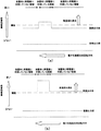
本発明者らは、上記2つの現象が生じるメカニズムを下記のように推察した。図1(a)および(b)を用いて、推察したメカニズムを説明する。 The present inventors inferred the mechanism by which the above two phenomena occur as follows. The inferred mechanism will be described with reference to FIGS. 1 (a) and 1 (b).
図1(a)は、Aの現象を説明するための模式的な説明図であり、電子写真感光体の表面に吸着した吸着物質の吸着量と高湿流れ発生の関係を示したものである。帯電生成物や水分などの吸着物質の吸着量が高湿流れ発生の閾値を超えると、画像上に高湿流れが発生する。
まず、画像出力前の初期の段階では、電子写真感光体の表面の吸着物質は少ない。次に、画像出力を繰り返し行った画像出力後の状態を考える。この状態では主に帯電の影響により、電子写真感光体の表面層が酸化され、電子写真感光体の表面には極性基が生成されることになる。この極性基が生成されることの高湿流れに対する影響は、次の2とおりの作用が考えられる。
まず、第1に、極性基それ自体が水分の吸着量を増大させることにより、電子写真感光体の表面の低抵抗化を起こしやすくする作用である。
第2に、極性基が生成されることにより、電子写真感光体の表面を帯電生成物が吸着しやすい表面へと変化させる作用である。帯電生成物は水分を吸着することで、電子写真感光体の表面の低抵抗化をより促進すると考えられている。
これら2つの相乗的な作用により、帯電生成物や水分などの吸着物質が増加し、高湿流れが発生しやすい状況を作り出すものと考えられる。
次に、この状態で、電子写真感光体を電子写真装置内に放置した場合を考える。放置時に帯電器に対面している領域では、帯電器周辺に多量の帯電生成物が存在していることに加え、酸化により帯電生成物が吸着しやすくなっているため、電子写真感光体の表面には大量の帯電生成物が吸着することになる。その結果、帯電生成物や水分などの吸着物質の吸着量が閾値を超えてしまい、高湿流れが発生すると考えられる。一方、放置時に帯電器に対面していない領域では、酸化によって帯電生成物や水分の吸着性が増大しているものの、付着すべき帯電生成物の存在量が少ないため、吸着物質の吸着量が閾値を超えるまでには至らない。
以上の結果、帯電器下流れが発生すると考えられる。
FIG. 1A is a schematic explanatory diagram for explaining the phenomenon A, and shows the relationship between the amount of adsorbed material adsorbed on the surface of the electrophotographic photosensitive member and the generation of a high-humidity flow. . When the adsorbed amount of the adsorbed substance such as the charged product or moisture exceeds the high humidity flow generation threshold, the high humidity flow is generated on the image.
First, in the initial stage before image output, there is little adsorbed material on the surface of the electrophotographic photosensitive member. Next, a state after image output in which image output is repeatedly performed will be considered. In this state, the surface layer of the electrophotographic photosensitive member is oxidized mainly due to the influence of charging, and polar groups are generated on the surface of the electrophotographic photosensitive member. The following two effects can be considered as the influence of the generation of the polar group on the high-humidity flow.
First, the polar group itself has the effect of easily reducing the resistance of the surface of the electrophotographic photosensitive member by increasing the amount of moisture adsorbed.
The second function is to change the surface of the electrophotographic photosensitive member to a surface on which the charged product is easily adsorbed by the generation of polar groups. It is thought that the charged product further promotes lowering the resistance of the surface of the electrophotographic photosensitive member by adsorbing moisture.
These two synergistic actions are considered to increase the amount of adsorbed substances such as charged products and moisture, creating a situation where high-humidity flows are likely to occur.
Next, consider a case where the electrophotographic photosensitive member is left in the electrophotographic apparatus in this state. In the area facing the charger when left unattended, in addition to the presence of a large amount of charged product around the charger, the charged product is easily adsorbed by oxidation. A large amount of charged product is adsorbed on the surface. As a result, it is considered that the amount of adsorption of adsorbed substances such as charged products and moisture exceeds a threshold value, and a high-humidity flow is generated. On the other hand, in the region that does not face the charger when left unattended, the adsorption of charged products and moisture has increased due to oxidation. The threshold is not exceeded.
As a result of the above, it is considered that a flow under the charger occurs.
図1(b)は、Bの現象を説明するための模式的な説明図であり、図1(a)と同様に電子写真感光体の表面に吸着した吸着物質の吸着量と高湿流れ発生の関係を示したものである。図1(a)との相違は、図1(a)に示した場合よりも長期にわたって画像形成を繰り返した状況を示している点である。a−SiC表面層の表面は、長期間にわたり繰り返し行われてきた帯電の影響により、図1(a)の場合に比べて酸化がさらに進行し、帯電生成物や水分の吸着性がさらに増加する。そのため、帯電生成物が多量に存在する放置時に帯電器に対面する部分はもとより、もともと帯電生成物の少ない放置時に帯電器に対面していない部分であっても、主として水分の吸着量の増加により、吸着物質の吸着量が閾値を超えてしまうことになる。結果として、放置時に帯電器に対面していない領域でも高湿流れが発生すると考えられる。 FIG. 1B is a schematic explanatory diagram for explaining the phenomenon of B. As in FIG. 1A, the amount of adsorbed material adsorbed on the surface of the electrophotographic photosensitive member and the generation of high-humidity flow. This shows the relationship. The difference from FIG. 1A is that the image formation is repeated over a longer period than in the case shown in FIG. The surface of the a-SiC surface layer is further oxidized as compared with the case of FIG. 1A due to the influence of charging that has been repeatedly performed over a long period of time, and the adsorptivity of the charged product and moisture is further increased. . Therefore, not only the part that faces the charger when left with a large amount of charged product, but also the part that does not face the charger when left with little charged product, mainly due to an increase in the amount of moisture adsorbed. Therefore, the amount of adsorption of the adsorbing substance exceeds the threshold value. As a result, it is considered that a high-humidity flow is generated even in a region that does not face the charger when left standing.
以上のように、高湿流れには、帯電器下流れと耐久流れの2つの要素があることが明らかとなったが、上述のように、その原因は、どちらも帯電生成物や水分の吸着量の増大であるということができる。よって、帯電器下流れおよび耐久流れを両方とも抑制するためには、吸着物質の吸着性を左右するa−SiC表面層の酸化を抑制することが極めて重要であることがわかった。
a−SiC表面層の酸化を抑制することにより、帯電生成物や水分などの吸着量の抑制が可能となる。このため、a−SiC表面層の表面の酸化層や吸着物質を除去するために摩耗量を増加させる必要がなくなり、電子写真感光体の良好な耐摩耗性を維持することができる。
As described above, it has been clarified that the high-humidity flow has two elements, namely, the flow under the charger and the durable flow. As described above, the cause of both is the adsorption of charged products and moisture. It can be said that the amount is increased. Therefore, it was found that in order to suppress both the flow under the charger and the durable flow, it is extremely important to suppress the oxidation of the a-SiC surface layer that affects the adsorptivity of the adsorbed substance.
By suppressing the oxidation of the a-SiC surface layer, it is possible to suppress the amount of adsorption of charged products and moisture. For this reason, it is not necessary to increase the amount of wear in order to remove the oxide layer and the adsorbed material on the surface of the a-SiC surface layer, and the good wear resistance of the electrophotographic photosensitive member can be maintained.
そこで、本発明者らは、a−SiC表面層の帯電による酸化を抑制することにより、従来に比べて吸着物質の付着を低減しつつ、耐摩耗性に優れたa−SiC表面層を形成することができると考え、鋭意検討を行った。その結果、a−SiC表面層を構成するケイ素原子の原子数と炭素原子の原子数との和に対する炭素原子の原子数の比を特定の範囲内にしたうえで、ケイ素原子の原子密度と炭素原子の原子密度との和を特定の値より大きくすることにより、上述の課題に対して大きな効果があることを見出し、本発明を完成させるに至った。
本発明の電子写真感光体は、上述のとおり、
光導電層と、該光導電層上の水素化アモルファスシリコンカーバイトで構成された表面層(a−SiC表面層)とを有し、
a−SiC表面層におけるケイ素原子の原子数(Si)と炭素原子の原子数(C)との和(Si+C)に対する炭素原子の原子数(C)の比(C/(Si+C))が0.61以上0.75以下であること、および、
a−SiC表面層におけるケイ素原子の原子密度と炭素原子の原子密度との和が6.60×10²²原子/cm3以上であること
を特徴としている。なお、ケイ素原子の原子数と炭素原子の原子数との和に対する炭素原子の原子数の比を、以下「C/(Si+C)」とも表記する。また、ケイ素原子の原子密度を、以下「Si原子密度」とも表記する。また、炭素原子の原子密度を、以下「C原子密度」とも表記する。また、ケイ素原子の原子密度と炭素原子の原子密度との和を、以下「Si+C原子密度」とも表記する。
Therefore, the inventors of the present invention form an a-SiC surface layer having excellent wear resistance while suppressing the adhesion of the adsorbing substance as compared with the conventional case by suppressing oxidation due to charging of the a-SiC surface layer. We thought that it was possible to do so, and intensively studied. As a result, after the ratio of the number of carbon atoms to the sum of the number of silicon atoms and the number of carbon atoms constituting the a-SiC surface layer is within a specific range, the atomic density of carbon atoms and carbon By making the sum of the atomic density of atoms larger than a specific value, it has been found that there is a great effect on the above-mentioned problems, and the present invention has been completed.
The electrophotographic photoreceptor of the present invention is as described above.
A photoconductive layer and a surface layer (a-SiC surface layer) composed of hydrogenated amorphous silicon carbide on the photoconductive layer;
The ratio of the number of carbon atoms (C) to the sum (Si + C) of the number of silicon atoms (Si) and the number of carbon atoms (C) in the a-SiC surface layer (C / (Si + C)) is 0. 61 or more and 0.75 or less, and
The sum of the atomic density of silicon atoms and the atomic density of carbon atoms in the a-SiC surface layer is 6.60 × 10 22 atoms / cm 3 or more. The ratio of the number of carbon atoms to the sum of the number of silicon atoms and the number of carbon atoms is hereinafter also expressed as “C / (Si + C)”. Further, the atomic density of silicon atoms is hereinafter also expressed as “Si atomic density”. Further, the atomic density of carbon atoms is hereinafter also expressed as “C atomic density”. Further, the sum of the atomic density of silicon atoms and the atomic density of carbon atoms is hereinafter also expressed as “Si + C atomic density”.
(表面層)
a−SiC表面層におけるSi+C原子密度を6.60×10²²原子/cm3以上にすることにより、耐高湿流れ性および耐摩耗性が大きく向上する。この理由を、以下に示す。
すなわち、a−SiCの酸化反応は、a−SiCの炭素原子の酸化および脱離によりケイ素原子と炭素原子との結合が切断され、新たに生成したケイ素原子のダングリングボンドに酸化物質が反応することによって生じる。この点、本発明によれば、a−SiC表面層におけるSi+C原子密度を大きくすることにより、ケイ素原子と炭素原子との結合を切断されにくくすることが可能になる。また、Si+C原子密度が大きくなることにより、a−SiC表面層における空間率が低減するため、炭素原子と酸化物質との反応確率が低減する。電子写真プロセスにおいては、帯電工程により生成したイオン種と炭素原子との反応により、炭素原子の酸化および脱離が生じると考えられる。よって、炭素原子の酸化を抑制することにより、ケイ素原子の酸化も抑制される。
本発明によれば、a−SiC表面層の構成原子間の距離が短縮され、空間率が低減されるため、a−SiC表面層の表面の酸化が抑制され、a−SiC表面層の表面での極性基の生成が抑制されると考えられる。この結果、高湿流れの抑制が可能となる。
また、a−SiC表面層の構成原子の結合力が高くなるため、a−SiC表面層の硬度は高くなり、その結果、電子写真感光体の耐摩耗性も向上すると考えられる。
以上の観点から、a−SiC表面層におけるSi+C原子密度は高い方が好ましく、6.81×10²²原子/cm3以上にすることで、耐高湿流れ性と耐摩耗性がより向上する。なお、a−SiCにおいては、最も高密度化した状態であるSiC結晶の13.0×1022原子/cm3という原子密度が、Si+C原子密度の上限となる。
(Surface layer)
By setting the Si + C atom density in the a-SiC surface layer to 6.60 × 10 22 atoms / cm 3 or more, the high-humidity flow resistance and the wear resistance are greatly improved. The reason is as follows.
That is, in the oxidation reaction of a-SiC, the bond between the silicon atom and the carbon atom is cut by oxidation and elimination of the carbon atom of a-SiC, and the oxidized substance reacts with the dangling bond of the newly generated silicon atom. Caused by In this regard, according to the present invention, by increasing the Si + C atom density in the a-SiC surface layer, the bond between the silicon atom and the carbon atom can be made difficult to be broken. Moreover, since the spatial rate in the a-SiC surface layer is reduced by increasing the Si + C atom density, the reaction probability between the carbon atom and the oxidizing substance is reduced. In the electrophotographic process, it is considered that oxidation and desorption of carbon atoms occur due to the reaction between ionic species generated in the charging step and carbon atoms. Therefore, by suppressing the oxidation of carbon atoms, the oxidation of silicon atoms is also suppressed.
According to the present invention, the distance between constituent atoms of the a-SiC surface layer is shortened and the space ratio is reduced, so that the oxidation of the surface of the a-SiC surface layer is suppressed, and the surface of the a-SiC surface layer is reduced. It is thought that the formation of polar groups is suppressed. As a result, the high humidity flow can be suppressed.
Further, since the bonding force of the constituent atoms of the a-SiC surface layer is increased, the hardness of the a-SiC surface layer is increased, and as a result, it is considered that the abrasion resistance of the electrophotographic photosensitive member is also improved.
From the above viewpoint, the Si + C atom density in the a-SiC surface layer is preferably higher, and by making it 6.81 × 10 22 atoms / cm 3 or more, high-humidity flow resistance and wear resistance are further improved. In a-SiC, the atomic density of 13.0 × 10 22 atoms / cm 3 of the SiC crystal in the most dense state is the upper limit of the Si + C atomic density.
また、a−SiC表面層におけるSi+C原子密度を上記範囲にしたうえで、さらに、a−SiC表面層におけるC/(Si+C)を0.61以上0.75以下にすることが、優れた電子写真感光体特性を得るうえで必要である。
a−SiC表面層において、C/(Si+C)を0.61よりも小さくすると、特に、原子密度の高いa−SiCを作製した場合、a−SiCの抵抗が低下する場合がある。このような場合、静電潜像形成時にキャリアが表面層中で横流れを生じやすくなる。そのため、静電潜像として孤立ドットを形成した場合に、表面層中でのキャリアの横流れにより孤立ドットが小さくなる。その結果、出力された画像において、特に、低濃度側での画像濃度が低下してしまうために、階調性の低下を生じる場合がある。このような理由により、本発明のような原子密度の高いa−SiC表面層においては、C/(Si+C)を0.61以上にする必要がある。
また、C/(Si+C)を0.75より大きくすると、特に、原子密度の高いa−SiCを作製した場合、a−SiC表面層での光吸収が急激に増加する場合がある。このような場合、静電潜像形成時に必要となる画像露光光の光量が多くなり、感度が極端に低下してしまう。また、a−SiC表面層の摩耗量に対する感度変動が大きくなることから、電子写真感光体に削れムラが生じた場合に、画像濃度ムラが生じる場合がある。このような理由により、本発明のような原子密度の高いa−SiC表面層においては、C/(Si+C)を0.75以下にする必要がある。
Moreover, after making the Si + C atom density in an a-SiC surface layer into the said range, it is further excellent electrophotography that C / (Si + C) in an a-SiC surface layer shall be 0.61 or more and 0.75 or less. Necessary for obtaining the photoreceptor characteristics.
When C / (Si + C) is made smaller than 0.61 in the a-SiC surface layer, particularly when a-SiC having a high atomic density is produced, the resistance of a-SiC may decrease. In such a case, the carrier tends to cause a lateral flow in the surface layer when forming the electrostatic latent image. Therefore, when an isolated dot is formed as an electrostatic latent image, the isolated dot becomes smaller due to the lateral flow of carriers in the surface layer. As a result, in the output image, particularly, the image density on the low density side is lowered, so that gradation may be lowered. For this reason, in the a-SiC surface layer having a high atomic density as in the present invention, C / (Si + C) needs to be 0.61 or more.
Further, when C / (Si + C) is larger than 0.75, particularly when a-SiC having a high atomic density is produced, light absorption in the a-SiC surface layer may increase rapidly. In such a case, the amount of image exposure light necessary for forming the electrostatic latent image increases, and the sensitivity is extremely lowered. In addition, since the sensitivity fluctuation with respect to the wear amount of the a-SiC surface layer becomes large, when the electrophotographic photosensitive member is shaved and uneven, image density unevenness may occur. For this reason, in the a-SiC surface layer having a high atomic density as in the present invention, C / (Si + C) needs to be 0.75 or less.
以上の理由により、好ましい電子写真感光体特性を維持しつつ、a−SiC表面層の耐酸化性を向上させて高湿流れを抑制するためには、a−SiC表面層におけるSi+C原子密度を6.60×10²²原子/cm3以上にし、かつ、a−SiC表面層におけるC/(Si+C)を0.61以上0.75以下にする必要がある。 For the above reasons, in order to improve the oxidation resistance of the a-SiC surface layer and suppress the high-humidity flow while maintaining preferable electrophotographic photoreceptor characteristics, the Si + C atom density in the a-SiC surface layer is set to 6 .60 × 10 22 atoms / cm 3 or more, and C / (Si + C) in the a-SiC surface layer must be 0.61 or more and 0.75 or less.
また、本発明においては、a−SiC表面層におけるケイ素原子の原子数(Si)と炭素原子の原子数(C)と水素原子の原子数(H)との和(Si+C+H)に対する水素原子の原子数(H)の比(H/(Si+C+H))を0.30以上0.45以下にすることが好ましい。これにより、電子写真感光体特性がさらに良好で、耐高湿流れ性および耐摩耗性にさらに優れた電子写真感光体が得られる。なお、ケイ素原子の原子数と炭素原子の原子数と水素原子の原子数との和に対する水素原子の原子数の比を、以下「H/(Si+C+H)」とも表記する。
原子密度の高いa−SiC表面層においては、光学的バンドギャップが狭くなり、光吸収が増加することにより感度が低下する場合がある。しかしながら、a−SiC表面層におけるH/(Si+C+H)を0.30以上含有させることで、光学的バンドギャップが広がり、感度の向上を図ることができる。
一方、a−SiC表面層におけるH/(Si+C+H)を0.45より多くすると、a−SiC表面層中には、メチル基のような水素原子の多い終端基が増加する傾向が見られる。メチル基のような複数の水素原子を有する終端基がa−SiC表面層中に多く存在すると、a−SiCの構造中に大きな空間を形成するとともに、周囲に存在する原子間の結合にひずみを生じさせる。このような構造上弱い部分は、酸化に対して弱い部分となってしまうと考えられる。また、水素原子をa−SiC表面層中に多量に含有させると、a−SiC表面層の骨格原子であるケイ素原子と炭素原子とのネットワーク化の促進が図りづらくなる。
このような理由により、H/(Si+C+H)を0.45以下にすることで、a−SiC表面層における骨格原子であるケイ素原子と炭素原子のネットワーク化の促進および原子間の結合に生じていたひずみの低減が可能となると考えられる。その結果、a−SiC表面層の耐酸化性がさらに向上し、電子写真感光体の耐摩耗性がさらに向上する。
In the present invention, the number of hydrogen atoms relative to the sum (Si + C + H) of the number of silicon atoms (Si), the number of carbon atoms (C), and the number of hydrogen atoms (H) in the a-SiC surface layer It is preferable that the ratio (H / (Si + C + H)) of the number (H) is 0.30 or more and 0.45 or less. As a result, an electrophotographic photoreceptor having further excellent electrophotographic photoreceptor characteristics and further excellent high-humidity flow resistance and wear resistance can be obtained. The ratio of the number of hydrogen atoms to the sum of the number of silicon atoms, the number of carbon atoms, and the number of hydrogen atoms is hereinafter also expressed as “H / (Si + C + H)”.
In an a-SiC surface layer having a high atomic density, the optical band gap is narrowed, and the sensitivity may be lowered due to increased light absorption. However, by containing H / (Si + C + H) in the a-SiC surface layer at 0.30 or more, the optical band gap is widened, and the sensitivity can be improved.
On the other hand, when H / (Si + C + H) in the a-SiC surface layer is more than 0.45, a termination group having many hydrogen atoms such as a methyl group tends to increase in the a-SiC surface layer. When many terminal groups having a plurality of hydrogen atoms such as methyl groups are present in the a-SiC surface layer, a large space is formed in the structure of the a-SiC, and the bonds between the surrounding atoms are distorted. Cause it to occur. Such a structurally weak part is considered to be a part weak against oxidation. Further, when a large amount of hydrogen atoms are contained in the a-SiC surface layer, it becomes difficult to promote networking of silicon atoms and carbon atoms, which are skeleton atoms of the a-SiC surface layer.
For these reasons, when H / (Si + C + H) is set to 0.45 or less, it has occurred in the promotion of networking of silicon atoms and carbon atoms, which are skeletal atoms, in the a-SiC surface layer and the bonding between the atoms. It is considered that the strain can be reduced. As a result, the oxidation resistance of the a-SiC surface layer is further improved, and the wear resistance of the electrophotographic photosensitive member is further improved.
また、本発明においては、a−SiC表面層のラマンスペクトルにおける1480cm−1のピーク強度(IG)に対する1390cm−1のピーク強度(ID)の比(ID/IG)を0.20以上0.70以下にすることが好ましい。なお、ラマンスペクトルにおける1480cm−1のピーク強度に対する1390cm−1のピーク強度の比を、以下「ID/IG」とも表記する。 In the present invention, the ratio of the peak intensity of 1390 cm -1 to the peak intensity (I G) of 1480 cm -1 in the Raman spectrum of the a-SiC surface layer (I D) and (I D / I G) 0.20 It is preferable to set it to 0.70 or less. Incidentally, the ratio of the peak intensity of 1390 cm -1 to the peak intensity of 1480 cm -1 in the Raman spectrum is hereinafter also expressed as "I D / I G".
まず、a−SiC表面層のラマンスペクトルについて、ダイヤモンドライクカーボンと比較しながら説明する。なお、ダイヤモンドライクカーボンを、以下「DLC」とも表記する。
sp3構造とsp2構造から形成されているDLCのラマンスペクトルは、1540cm−1付近に主ピークを持ち、1390cm−1付近にショルダーバンドを有する非対称なラマンスペクトルが観察される。RF−CVD法で形成されたa−SiC表面層では、1480cm−1付近に主ピークを持ち、1390cm−1付近にショルダーバンドを有するDLCに類似したラマンスペクトルが観察される。a−SiC表面層の主ピークがDLCよりも低波数側にシフトしているのは、a−SiC表面層にはケイ素原子が含まれているためである。このことから、RF−CVD法で形成されたa−SiC表面層は、DLCに非常に近い構造を有する材料であることがわかる。
一般的に、DLCのラマンスペクトルにおいて、高波数バンドのピーク強度に対する低波数バンドのピーク強度の比が小さいほど、DLCのsp3性が高い傾向があることが知られている。よって、a−SiC表面層においても、DLCと非常に近い構造であることから、高波数バンドのピーク強度に対する低波数バンドのピーク強度の比が小さいほど、sp3性が高い傾向を示すと考えられる。
First, the Raman spectrum of the a-SiC surface layer will be described in comparison with diamond-like carbon. The diamond-like carbon is hereinafter also referred to as “DLC”.
Raman spectra of DLC formed of sp 3 structure and sp 2 structure has a main peak near 1540 cm -1, asymmetrical Raman spectrum having a shoulder band is observed around 1390 cm -1. The a-SiC surface layer formed by RF-CVD method has a major peak around 1480 cm -1, the Raman spectrum similar to the DLC having a shoulder band around 1390 cm -1 is observed. The main peak of the a-SiC surface layer is shifted to the lower wavenumber side than DLC because the a-SiC surface layer contains silicon atoms. This shows that the a-SiC surface layer formed by the RF-CVD method is a material having a structure very close to DLC.
In general, it is known that in the Raman spectrum of DLC, the smaller the ratio of the peak intensity of the low wave number band to the peak intensity of the high wave number band, the higher the sp 3 property of DLC. Therefore, since the a-SiC surface layer has a structure very close to DLC, it is considered that the smaller the ratio of the peak intensity of the low wave number band to the peak intensity of the high wave number band, the higher the sp 3 property. It is done.
本発明の原子密度の高いa−SiC表面層において、a−SiC表面層におけるID/IGを0.70以下にすることにより、耐高湿流れ性および耐摩耗性をさらに向上させることができる。
この理由としては、sp3性が向上すると、sp2の2次元のネットワーク数が減少し、sp3の3次元ネットワークが増加するため、骨格原子の結合数が増加し、強固な構造体が形成可能になるためだと考えている。
そのため、a−SiC表面層におけるID/IGは小さい方がより好ましいが、量産レベルで形成されるa−SiC表面層では、完全にsp2構造を取り除くことはできない。そのため、本発明においては、a−SiC表面層におけるID/IGの下限値を、本実施例において耐高湿流れ性および耐摩耗性の向上が確認された0.2としている。
In atomic dense a-SiC surface layer of the present invention, by the I D / I G in the a-SiC surface layer to 0.70 or less, further improving the high-humidity image flow resistance and wear resistance it can.
The reason for this is that if the sp 3 property is improved, the number of sp 2 two-dimensional networks decreases and the number of sp 3 three-dimensional networks increases, so the number of skeletal atoms increases and a strong structure is formed. I think it is possible.
Therefore, although it is more preferred I D / I G is small in the a-SiC surface layer, the a-SiC surface layer formed by mass production level, can not be removed completely sp 2 structure. Therefore, in the present invention, the lower limit value of I D / I G in the a-SiC surface layer is set to 0.2 in which improvement in high-humidity flow resistance and wear resistance is confirmed in this example.
また、本発明においては、クリーニングブレードによる電子写真感光体の表面のクリーニング性の観点から、原子間力顕微鏡(AFM)により電子写真感光体の表面を10μm×10μmの範囲で測定したときに得られる微視的形状から求められる表面粗さRaは、10nm以上80nm以下であることが好ましく、10nm以上50nm以下であることがより好ましい。なお、表面粗さRaを、以下単に「Ra」とも表記する。
また、上記と同様のクリーニング性の観点から、AFMにより電子写真感光体の表面を10μm×10μmの範囲で測定したときに得られる微視的形状から求められる平均傾斜Δaは、0.10以上0.40以下あることが好ましい。なお、平均傾斜Δaを、以下単に「Δa」とも表記する。
In the present invention, the surface of the electrophotographic photosensitive member is measured with an atomic force microscope (AFM) in the range of 10 μm × 10 μm from the viewpoint of the cleaning property of the surface of the electrophotographic photosensitive member by the cleaning blade. The surface roughness Ra obtained from the microscopic shape is preferably 10 nm or more and 80 nm or less, and more preferably 10 nm or more and 50 nm or less. Hereinafter, the surface roughness Ra is also simply expressed as “Ra”.
In addition, from the viewpoint of the same cleaning property as described above, the average inclination Δa obtained from the microscopic shape obtained when the surface of the electrophotographic photosensitive member is measured in the range of 10 μm × 10 μm by AFM is 0.10 or more and 0. .40 or less is preferable. The average inclination Δa is also simply expressed as “Δa” hereinafter.
本発明において、上記a−SiC表面層の形成方法は、上記規定を満足する層を形成できるものであればいずれの方法であってもよい。具体的には、プラズマCVD法、真空蒸着法、スパッタリング法、イオンプレーティング法などが挙げられる。これらの中でも、原料供給の容易さなどの点で、プラズマCVD法が好ましい。 In the present invention, the method for forming the a-SiC surface layer may be any method as long as it can form a layer that satisfies the above definition. Specific examples include plasma CVD, vacuum deposition, sputtering, and ion plating. Among these, the plasma CVD method is preferable from the viewpoint of easy supply of raw materials.
a−SiC表面層の形成方法としてプラズマCVD法を選択した場合、a−SiC表面層の形成方法は以下のとおりである。
すなわち、ケイ素原子供給用の原料ガスおよび炭素原子供給用の原料ガスを、内部を減圧にしうる反応容器内に所望のガス状態で導入し、該反応容器内にグロー放電を生起させる。これによって、該反応容器内に導入した原料ガスを分解し、あらかじめ所定の位置に設置された基体上にa−SiCで構成された層を形成すればよい。
ケイ素原子供給用の原料ガスとしては、たとえば、シラン(SiH4)、ジシラン(Si2H6)などのシラン類が好適に使用できる。また、炭素原子供給用の原料ガスとしては、たとえば、メタン(CH4)、アセチレン(C2H2)などのガスが好適に使用できる。また、主にH/(Si+C+H)を調整するためとして、水素(H2)を、上記の原料ガスとともに使用してもよい。
When the plasma CVD method is selected as the method for forming the a-SiC surface layer, the method for forming the a-SiC surface layer is as follows.
That is, a raw material gas for supplying silicon atoms and a raw material gas for supplying carbon atoms are introduced in a desired gas state into a reaction vessel whose inside can be depressurized to cause glow discharge in the reaction vessel. In this way, the source gas introduced into the reaction vessel is decomposed, and a layer composed of a-SiC may be formed on a substrate previously set at a predetermined position.
As a source gas for supplying silicon atoms, for example, silanes such as silane (SiH 4 ) and disilane (Si 2 H 6 ) can be preferably used. As the source gas for the carbon atoms supplied, for example, methane (CH 4), acetylene (C 2 H 2) gas or the like can be suitably used. Moreover, hydrogen (H 2 ) may be used together with the above-mentioned source gas mainly for adjusting H / (Si + C + H).
本発明のa−SiC表面層を形成する場合においては、反応容器に供給するガス流量を少なく、高周波電力を高く、または、基体の温度を高くすることにより、Si+C原子密度が高くなる傾向がある。実際は、これらの条件を適宜組み合わせて設定すればよい。 When the a-SiC surface layer of the present invention is formed, the Si + C atom density tends to increase by decreasing the gas flow rate supplied to the reaction vessel, increasing the high-frequency power, or increasing the temperature of the substrate. . In practice, these conditions may be set in appropriate combination.
(光導電層)
本発明において、光導電層は、電子写真特性上の性能を満足できる光導電特性を有するものであればいずれのものであってもよいが、耐久性、安定性の観点から、水素化アモルファスシリコンで構成された光導電層が好ましい。なお、水素化アモルファスシリコンを、以下「a−Si」とも表記する。
(Photoconductive layer)
In the present invention, the photoconductive layer may be any one as long as it has photoconductive characteristics that can satisfy the performance on electrophotographic characteristics, but from the viewpoint of durability and stability, hydrogenated amorphous silicon. A photoconductive layer composed of is preferable. The hydrogenated amorphous silicon is hereinafter also expressed as “a-Si”.
本発明において、光導電層としてa−Siで構成された光導電層を用いる場合は、a−Si中の未結合手を補償するため、水素原子に加えて、ハロゲン原子を含有させることができる。
水素原子(H)およびハロゲン原子(X)の含有量の合計(H+X)は、ケイ素原子(Si)と水素原子(H)とハロゲン原子(X)との和(Si+H+X)に対して10原子%以上であることが好ましく、15原子%以上であることがより好ましい。一方、30原子%以下であることが好ましく、25原子%以下であることがより好ましい。
In the present invention, when a photoconductive layer composed of a-Si is used as the photoconductive layer, in order to compensate for dangling bonds in a-Si, halogen atoms can be contained in addition to hydrogen atoms. .
The total content (H + X) of the hydrogen atom (H) and the halogen atom (X) is 10 atomic% with respect to the sum (Si + H + X) of the silicon atom (Si), the hydrogen atom (H), and the halogen atom (X). It is preferable that it is above, and it is more preferable that it is 15 atomic% or more. On the other hand, it is preferably 30 atomic% or less, and more preferably 25 atomic% or less.
本発明において、光導電層には必要に応じて伝導性を制御するための原子を含有させることが好ましい。伝導性を制御するための原子は、光導電層中にまんべんなく均一に分布した状態で含有されていてもよいし、また、膜厚方向には不均一な分布状態で含有している部分があってもよい。
伝導性を制御するための原子としては、半導体分野における、いわゆる不純物を挙げることができる。すなわち、p型伝導性を与える周期表13族に属する原子またはn型伝導性を与える周期表15族に属する原子を用いることができる。周期表13族に属する原子の中でも、ホウ素原子、アルミニウム原子、ガリウム原子が好ましい。周期表15族に属する原子の中でも、リン原子、ヒ素原子が好ましい。
光導電層に含有される伝導性を制御するための原子の含有量は、ケイ素原子(Si)に対して1×10⁻²原子ppm以上であることが好ましく、5×10⁻²原子ppm以上であることがより好ましく、1×10⁻¹原子ppm以上であることがより一層好ましい。一方、1×10⁴原子ppm以下であることが好ましく、5×10³原子ppm以下であることがより好ましく、1×10³原子ppm以下であることがより一層好ましい。
In the present invention, the photoconductive layer preferably contains atoms for controlling conductivity as required. The atoms for controlling the conductivity may be contained in the photoconductive layer in a uniformly distributed state, or there may be a portion containing the nonuniform distribution in the film thickness direction. May be.
As atoms for controlling conductivity, so-called impurities in the semiconductor field can be given. That is, an atom belonging to Group 13 of the periodic table giving p-type conductivity or an atom belonging to Group 15 of the periodic table giving n-type conductivity can be used. Among atoms belonging to Group 13 of the periodic table, a boron atom, an aluminum atom, and a gallium atom are preferable. Among atoms belonging to Group 15 of the periodic table, a phosphorus atom and an arsenic atom are preferable.
The content of atoms for controlling conductivity contained in the photoconductive layer is preferably 1 × 10 −2 atom ppm or more with respect to silicon atoms (Si), and 5 × 10 −2 atom ppm or more. more preferably, it is more preferably 1 × 10 -1 atomic ppm or more. Meanwhile, 1 is preferably × 10 4 atom ppm or less, more preferably 5 × and 10 3 atom ppm or less, and still more preferably 1 × 10 3 atom ppm or less.
本発明において、光導電層の膜厚は、所望の電子写真特性が得られること、経済的効果などの点から、15μm以上であることが好ましく、20μm以上であることがより好ましい。一方、60μm以下であることが好ましく、50μm以下であることがより好ましく、40μm以下であることがより一層好ましい。光導電層の膜厚が15μm未満であると、帯電部材への通過電流量が増大し、劣化が早まりやすい傾向がある。光導電層の膜厚が60μmを超えると、a−Siの異常成長部位が大きくなることがあり、具体的には、水平方向で50〜150μm、高さ方向で5〜20μmとなり、表面を摺擦する部材へのダメージが無視できなくなる場合や、画像欠陥となる場合がある。 In the present invention, the film thickness of the photoconductive layer is preferably 15 μm or more, more preferably 20 μm or more from the viewpoints of obtaining desired electrophotographic characteristics and economic effects. On the other hand, it is preferably 60 μm or less, more preferably 50 μm or less, and even more preferably 40 μm or less. When the film thickness of the photoconductive layer is less than 15 μm, the amount of current passing through the charging member increases and the deterioration tends to be accelerated. When the thickness of the photoconductive layer exceeds 60 μm, the abnormal growth site of a-Si may become large, specifically 50 to 150 μm in the horizontal direction and 5 to 20 μm in the height direction. In some cases, damage to the rubbing member cannot be ignored, or an image defect may occur.
なお、光導電層は、単一の層で構成されてもよいし、複数の層(たとえば、電荷発生層と電荷輸送層)で構成されてもよい。 The photoconductive layer may be composed of a single layer or a plurality of layers (for example, a charge generation layer and a charge transport layer).
a−Siで構成された光導電層の形成方法としては、たとえば、プラズマCVD法、真空蒸着法、スパッタリング法、イオンプレーティング法などが挙げられる。これらの中でも、原料供給の容易さなどの点で、プラズマCVD法が好ましい。 Examples of a method for forming a photoconductive layer composed of a-Si include a plasma CVD method, a vacuum deposition method, a sputtering method, and an ion plating method. Among these, the plasma CVD method is preferable from the viewpoint of easy supply of raw materials.
以下、光導電層の形成方法について、プラズマCVD法を例にとって説明する。
光導電層を形成するには、ケイ素原子供給用の原料ガスおよび水素原子供給用の原料ガスを、内部を減圧にしうる反応容器内に所望のガス状態で導入し、該反応容器内にグロー放電を生起させる。これによって、該反応容器内に導入した原料ガスを分解し、あらかじめ所定の位置に設置された基体上にa−Siで構成された層を形成すればよい。
本発明において、ケイ素原子供給用の原料ガスとしては、たとえば、シラン(SiH4)、ジシラン(Si2H6)などのシラン類が好適に使用できる。また、水素原子供給用の原料ガスとしては、上記シラン類に加えて、たとえば、水素(H2)も好適に使用できる。
また、上述のハロゲン原子、伝導性を制御するための原子、炭素原子、酸素原子、窒素原子など光導電層を含有させる場合には、それぞれの原子を含むガス状または容易にガス化しうる物質を材料として適宜使用すればよい。
Hereinafter, a method for forming a photoconductive layer will be described by taking a plasma CVD method as an example.
In order to form a photoconductive layer, a raw material gas for supplying silicon atoms and a raw material gas for supplying hydrogen atoms are introduced into a reaction vessel that can be depressurized in a desired gas state, and glow discharge is performed in the reaction vessel. Wake up. Thus, the source gas introduced into the reaction vessel is decomposed, and a layer composed of a-Si may be formed on a substrate previously set at a predetermined position.
In the present invention, as a source gas for supplying silicon atoms, for example, silanes such as silane (SiH 4 ) and disilane (Si 2 H 6 ) can be preferably used. In addition to the above silanes, for example, hydrogen (H 2 ) can also be suitably used as the source gas for supplying hydrogen atoms.
In addition, when a photoconductive layer such as the above-described halogen atom, atom for controlling conductivity, carbon atom, oxygen atom, nitrogen atom or the like is included, a gaseous or easily gasifiable substance containing each atom is used. What is necessary is just to use suitably as a material.
(基体)
基体は、導電性を有し、表面に形成される光導電層および表面層を保持しうるものであれば特に限定されず、いずれのものであってもよい。基体の材質としては、たとえば、アルミニウム、鉄などの金属や、これらの合金などが挙げられる。なお、導電性を有する基体(導電性の基体)を、以下「導電性基体」とも表記する。
(Substrate)
The substrate is not particularly limited as long as it has conductivity and can hold the photoconductive layer formed on the surface and the surface layer, and any substrate may be used. Examples of the material of the substrate include metals such as aluminum and iron, and alloys thereof. Note that a conductive substrate (conductive substrate) is hereinafter also referred to as a “conductive substrate”.
(中間層)
本発明においては、光導電層と本発明のa−SiC表面層との間に中間層を設けることが好ましい。また、該中間層におけるC/(Si+C)を0.61以上0.75以下にし、該中間層におけるSi+C原子密度を5.50×1022原子/cm3以上6.45×1022原子/cm3以下にすることが好ましい。また、該中間層の膜厚は150nm以上であることが好ましい。
(Middle layer)
In the present invention, it is preferable to provide an intermediate layer between the photoconductive layer and the a-SiC surface layer of the present invention. Further, C / (Si + C) in the intermediate layer is set to 0.61 or more and 0.75 or less, and the Si + C atom density in the intermediate layer is set to 5.50 × 10 22 atoms / cm 3 or more and 6.45 × 10 22 atoms / cm. It is preferable to make it 3 or less. Further, the film thickness of the intermediate layer is preferably 150 nm or more.
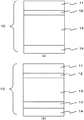
図5(a)は、本発明の電子写真感光体の層構成の一例を模式的に示した図である。図5(a)中、電子写真感光体10は、たとえばアルミニウムなどの円筒状で導電性の基体14と、基体14の表面に順次形成された光導電層13、中間層12および表面層11とを有している。
FIG. 5A is a diagram schematically showing an example of the layer structure of the electrophotographic photosensitive member of the present invention. In FIG. 5A, an electrophotographic
以下、上記中間層について詳細に説明する。
上記中間層は、本発明のa−SiC表面層と組み合わせることで、光導電層を機械的なストレスから保護し、圧傷を抑制する効果が得られる。
圧傷の原因は、使用中に電子写真装置内に何らかの理由で硬度の高い異物が噛み込まれで、電子写真感光体の表面に機械的なストレスを与えることにより発生すると考えられる。ただし、必ずしも電子写真感光体の表面の傷を伴うものではない。また、一度圧傷が発生した電子写真感光体を、たとえば200℃で1時間加熱することで、該圧傷が消失する場合も見られる。このため、電子写真感光体の表面そのものではなく、表面層を介して光導電層に過度のストレスが加わったために圧傷は発生するものと考えられる。このような圧傷は、高硬度の表面層を形成することにより発生を抑えることはできるが、光導電層へのストレスを抑制するためには、最低限度の膜厚が必要とされている。
電子写真感光体の表面層は、長期に渡る使用により次第に摩耗していくので、電子写真感光体の設定寿命終了後にも、上記の最低限度の膜厚を維持している必要がある。
Hereinafter, the intermediate layer will be described in detail.
By combining the intermediate layer with the a-SiC surface layer of the present invention, the effect of protecting the photoconductive layer from mechanical stress and suppressing the pressure scar can be obtained.
It is considered that the cause of the injuries is caused by mechanical stress being applied to the surface of the electrophotographic photosensitive member due to a foreign object having high hardness being caught in the electrophotographic apparatus for some reason during use. However, the surface of the electrophotographic photoreceptor is not necessarily accompanied by scratches. In addition, when the electrophotographic photosensitive member once has been injured is heated at, for example, 200 ° C. for 1 hour, the indentation may disappear. For this reason, it is considered that injuries occur because excessive stress is applied to the photoconductive layer through the surface layer, not the surface itself of the electrophotographic photosensitive member. Such crushing can be suppressed by forming a high-hardness surface layer, but a minimum film thickness is required to suppress stress on the photoconductive layer.
Since the surface layer of the electrophotographic photosensitive member is gradually worn by long-term use, it is necessary to maintain the above-mentioned minimum film thickness even after the set life of the electrophotographic photosensitive member is completed.
また、本発明のa−SiC表面層はSi+C原子密度を向上させたことにより、耐酸化性(耐高湿流れ性)および耐摩耗性を向上させたものであるが、上述のように光透過性はやや低い傾向にある。
そこで、光導電層と本発明のa−SiC表面層との間に中間層を設け、該中間層をSi+C原子密度が本発明のa−SiC表面層よりも低い、比較的光透過性に優れた膜とし、その膜厚を上記の最低限度の膜厚にすることにより、電子写真感光体の感度を向上させることができる。
The a-SiC surface layer of the present invention has improved oxidation resistance (high humidity flow resistance) and wear resistance by improving the Si + C atom density. Sex tends to be somewhat low.
Therefore, an intermediate layer is provided between the photoconductive layer and the a-SiC surface layer of the present invention, and the intermediate layer has a Si + C atom density lower than that of the a-SiC surface layer of the present invention and relatively excellent in light transmittance. The sensitivity of the electrophotographic photosensitive member can be improved by setting the film thickness to the minimum film thickness described above.
また、中間層におけるSi+C原子密度を、本発明のa−SiC表面層におけるSi+C原子密度よりも小さくすることで、a−SiC表面層が受ける機械的なストレスを中間層により効果的に緩和できると推測される。そのため、中間層を設けない場合に比べて、より効果的に圧傷を抑制することができる。 Moreover, when the Si + C atom density in the intermediate layer is made smaller than the Si + C atom density in the a-SiC surface layer of the present invention, the mechanical stress applied to the a-SiC surface layer can be effectively reduced by the intermediate layer. Guessed. Therefore, compared with the case where an intermediate layer is not provided, it is possible to suppress the injuries more effectively.
以上の効果を得るためには、中間層は原子密度とSi+C原子密度を本発明のa−SiC表面層よりも低くする必要があるが、Si+C原子密度があまり低くなると、中間層の圧傷抑制能が損なわれてくる。これは、中間層が効果的にストレスを緩和するには、表面層におけるSi+C原子密度とのバランスにおいて最適な範囲があるためと考えられる。そのため、本発明においては、中間層におけるSi+C原子密度の下限値を、圧傷抑制の効果が確認された5.50×10²²原子/cm3としている。 In order to obtain the above effects, the intermediate layer needs to have lower atomic density and Si + C atomic density than the a-SiC surface layer of the present invention. The ability is impaired. This is presumably because the intermediate layer has an optimum range in balance with the Si + C atom density in the surface layer in order to effectively relieve the stress. For this reason, in the present invention, the lower limit value of the Si + C atom density in the intermediate layer is set to 5.50 × 10 22 atoms / cm 3 in which the effect of suppressing the scratching is confirmed.
また、中間層におけるC/(Si+C)の効果は、本発明のa−SiC表面層における効果とほぼ同じである。すなわち、C/(Si+C)が小さくなると、中間層の抵抗が下がりやすくなり、ドット再現性の低下による濃度低下が起こりやすい。また、C/(Si+C)がある程度より大きくなると光透過性が低減し、Si+C原子密度を小さくすることによる感度向上の効果が小さくなる。したがって、中間層におけるC/(Si+C)は0.61以上0.75以下にすることが好ましい。 Further, the effect of C / (Si + C) in the intermediate layer is substantially the same as the effect in the a-SiC surface layer of the present invention. That is, when C / (Si + C) becomes small, the resistance of the intermediate layer is likely to decrease, and the density is likely to decrease due to a decrease in dot reproducibility. Further, when C / (Si + C) is larger than a certain level, the light transmittance is reduced, and the effect of improving the sensitivity by reducing the Si + C atom density is reduced. Therefore, C / (Si + C) in the intermediate layer is preferably 0.61 or more and 0.75 or less.
また、中間層は上述のように圧傷抑制のため、最低限の膜厚が必要であるが、本発明では、上記中間層の膜厚を150nm以上にすることで明らかな圧傷抑制効果を得ることができた。なお、上記中間層の膜厚は、圧傷抑制効果を得るための上限値はないが、中間層が厚ければそれだけ光透過性が損なわれる結果となる。具体的には、150nmの膜厚で、使用する電子写真プロセスにあわせて決定すればよいが、おおよそ700nm以下にすることが好ましい。 Further, as described above, the intermediate layer needs to have a minimum film thickness in order to suppress the injuries. However, in the present invention, the intermediate layer has a film thickness of 150 nm or more, and thus has an obvious effect of suppressing the injuries. I was able to get it. In addition, the film thickness of the intermediate layer has no upper limit value for obtaining the effect of suppressing crushing. However, the thicker the intermediate layer, the more the light transmittance is impaired. Specifically, it may be determined in accordance with the electrophotographic process to be used with a film thickness of 150 nm, but is preferably about 700 nm or less.
なお、本発明者の検討によれば、中間層の光透過性に対する影響はC/(Si+C)およびSi+C原子密度が支配的であり、H/(Si+C+H)の依存性はあまり見られなかった。これは、原子密度が表面層よりも低下していることにより、光透過性における水素原子の原子密度の依存性が低下したためと考えられる。なお、水素原子の原子密度を、以下「H原子密度」とも表記する。 According to the study by the present inventors, the influence on the light transmittance of the intermediate layer is dominated by C / (Si + C) and Si + C atom density, and the dependence of H / (Si + C + H) was not seen so much. This is presumably because the dependence of the atomic density of hydrogen atoms on the light transmittance is reduced because the atomic density is lower than that of the surface layer. The atomic density of hydrogen atoms is hereinafter also expressed as “H atomic density”.
以上のように、本発明のa−SiC表面層と上記中間層との組み合わせにより、耐高湿流れ性および耐摩耗性を向上させるとともに、圧傷を効果的に抑制し、さらには感度の改善を得られるものである。
一方、上記中間層には、本発明のa−SiC表面層のような耐高湿流れ性および耐摩耗性の向上効果は求められない。そのため、電子写真感光体の設定寿命経過時点において、本発明のa−SiC表面層が上記中間層上に残ることを想定する必要がある。一方、本発明のa−SiC表面層の膜厚は、上述のような圧傷抑制効果を考慮する必要はないため、使用する電子写真プロセスにもよるが、100nm以上あれば十分と推測される。
As described above, the combination of the a-SiC surface layer of the present invention and the intermediate layer improves high-humidity flow resistance and wear resistance, effectively suppresses crushing, and further improves sensitivity. Can be obtained.
On the other hand, the intermediate layer is not required to have the effect of improving the high-humidity flow resistance and wear resistance as in the a-SiC surface layer of the present invention. Therefore, it is necessary to assume that the a-SiC surface layer of the present invention remains on the intermediate layer when the set lifetime of the electrophotographic photosensitive member has elapsed. On the other hand, the film thickness of the a-SiC surface layer of the present invention does not need to take the above-described effect of suppressing the pressure scar into consideration, and depends on the electrophotographic process to be used. .
上記中間層を形成する方法としては、上述の表面層を形成する場合と同様の方法を採用することができる。そして、反応容器に供給するガス量、高周波電力、反応容器内の圧力、基体の温度などの条件を、必要に応じて表面層と異なる条件にすることで、形成される中間層の原子密度を調整すればよい。 As a method for forming the intermediate layer, the same method as that for forming the surface layer described above can be employed. And by changing the conditions such as the amount of gas supplied to the reaction vessel, the high frequency power, the pressure in the reaction vessel, the temperature of the substrate, etc. as necessary, the atomic density of the intermediate layer to be formed is changed. Adjust it.
(電荷注入阻止層)
本発明においては、基体と光導電層との間に基体側からの電荷の注入を阻止する働きを有する電荷注入阻止層を設けることが好ましい。すなわち、電荷注入阻止層は、電子写真感光体の表面が一定極性の帯電処理を受けた際、基体から光導電層への電荷の注入を阻止する機能を有する層である。このような機能を付与するために、電荷注入阻止層は、光導電層を構成する材料をベースとしたうえで、伝導性を制御するための原子を光導電層に比べて比較的多く含有させる。
伝導性を制御するために電荷注入阻止層に含有させる原子は、電荷注入阻止層中にまんべんなく均一に分布した状態で含有されていてもよいし、また、膜厚方向には不均一な分布状態で含有している部分があってもよい。分布濃度が不均一な場合には、基体側に多く分布するように含有させるのが好適である。いずれの場合においても、伝導性を制御するための原子が基体の表面に対して平行面内方向に均一な分布で電荷注入阻止層に含有されることが、特性の均一化を図る上からも好ましい。
伝導性を制御するために電荷注入阻止層に含有させる原子としては、帯電極性に応じて周期表13族または15族に属する原子を用いることができる。
さらに、電荷注入阻止層には、炭素原子、窒素原子および酸素原子のうち少なくとも1種の原子を含有させることにより、電荷注入阻止層を基体との間の密着性を向上させることができる。
電荷注入阻止層に含有される炭素原子、窒素原子および酸素原子のうち少なくとも1種の原子は、電荷注入阻止層中にまんべんなく均一に分布した状態で含有されていてもよいし、また、膜厚方向には均一に含有されてはいるが、不均一に分布する状態で含有している部分があってもよい。いずれの場合にも、伝導性を制御するための原子が基体の表面に対して平行面内方向に均一な分布で電荷注入阻止層に含有されることが、特性の均一化を図る上からも好ましい。
(Charge injection blocking layer)
In the present invention, it is preferable to provide a charge injection blocking layer having a function of blocking charge injection from the substrate side between the substrate and the photoconductive layer. That is, the charge injection blocking layer is a layer having a function of blocking the injection of charges from the substrate to the photoconductive layer when the surface of the electrophotographic photosensitive member is subjected to a charging process with a certain polarity. In order to provide such a function, the charge injection blocking layer is based on the material constituting the photoconductive layer, and contains a relatively large number of atoms for controlling conductivity compared to the photoconductive layer. .
The atoms contained in the charge injection blocking layer for controlling conductivity may be contained in the charge injection blocking layer evenly distributed or in a non-uniform distribution state in the film thickness direction. There may be a part contained in When the distribution concentration is non-uniform, it is preferable to contain it so that it is distributed more on the substrate side. In any case, the atoms for controlling the conductivity are contained in the charge injection blocking layer in a uniform distribution in the in-plane direction parallel to the surface of the substrate. preferable.
As atoms to be contained in the charge injection blocking layer in order to control conductivity, atoms belonging to Group 13 or 15 of the periodic table can be used depending on the charge polarity.
Further, the charge injection blocking layer can contain at least one kind of atom of carbon atom, nitrogen atom and oxygen atom, thereby improving the adhesion between the charge injection blocking layer and the substrate.
At least one kind of carbon atom, nitrogen atom and oxygen atom contained in the charge injection blocking layer may be contained in a state of being evenly distributed in the charge injection blocking layer. Although it is contained uniformly in the direction, there may be a portion containing it in a non-uniformly distributed state. In any case, the atoms for controlling the conductivity are contained in the charge injection blocking layer in a uniform distribution in the in-plane direction parallel to the surface of the substrate from the viewpoint of uniform characteristics. preferable.
電荷注入阻止層の膜厚は、所望の電子写真特性が得られること、経済的効果などの点から、0.1〜10μmであることが好ましく、0.3〜5μmであることがより好ましく、0.5〜3μmであることがより一層好ましい。膜厚を0.1μm以上にすることにより、基体からの電荷の注入阻止能を十分に有することができ、好ましい帯電能を得ることができる。一方、5μm以下にすることにより、電荷注入阻止層形成時間の延長による製造コストの増加を防ぐことができる。 The film thickness of the charge injection blocking layer is preferably from 0.1 to 10 μm, more preferably from 0.3 to 5 μm from the viewpoint of obtaining desired electrophotographic characteristics and economic effects. More preferably, it is 0.5-3 micrometers. By setting the film thickness to 0.1 μm or more, the charge injection ability from the substrate can be sufficiently obtained, and a preferable charging ability can be obtained. On the other hand, when the thickness is 5 μm or less, it is possible to prevent an increase in manufacturing cost due to extension of the charge injection blocking layer formation time.
また、本発明においては、光導電層と本発明のa−Si表面層との間に電荷注入阻止層を設けてもよい。
なお、光導電層の下に設けた電荷注入阻止層を、以下「下部電荷注入阻止層」とも表記する。また、光導電層の上に設けた電荷注入阻止層を、以下「上部電荷注入阻止層」とも表記する。
本発明において、上部電荷注入阻止層を光導電層上に設ける場合は、上記中間層は上部電荷注入阻止層と本発明のa−Si表面層との間に設けることが好ましい。
In the present invention, a charge injection blocking layer may be provided between the photoconductive layer and the a-Si surface layer of the present invention.
The charge injection blocking layer provided below the photoconductive layer is also referred to as a “lower charge injection blocking layer” hereinafter. Further, the charge injection blocking layer provided on the photoconductive layer is hereinafter also referred to as “upper charge injection blocking layer”.
In the present invention, when the upper charge injection blocking layer is provided on the photoconductive layer, the intermediate layer is preferably provided between the upper charge injection blocking layer and the a-Si surface layer of the present invention.
図5(b)に、下部電荷注入阻止層を形成した場合の電子写真感光体の層構成を模式的に示す。図5(b)において、電子写真感光体10は、基体14と、基体14上に順次形成された下部電荷注入阻止層15、光導電層13、中間層12および表面層11とを有している。
FIG. 5B schematically shows the layer structure of the electrophotographic photosensitive member when the lower charge injection blocking layer is formed. In FIG. 5B, the electrophotographic
また、上記各層の間では、それぞれの組成を連続的につなぐ、いわゆる変化層を必要に応じて設けることもできる。 In addition, a so-called change layer that continuously connects the respective compositions may be provided between the above layers as necessary.
<本発明の電子写真感光体を製造するための製造装置および製造方法>
図2は、本発明のa−Si感光体を作製するための高周波電源を用いたRFプラズマCVD法による電子写真感光体の堆積装置の一例を模式的に示した図である。
この堆積装置は、大別すると、反応容器3110を有する堆積装置3100、原料ガス供給装置3200、および、反応容器3110内を減圧する為の排気装置(図示せず)から構成されている。
堆積装置3100中の反応容器3110内にはアースに接続された基体3112、基体加熱用ヒーター3113、および、原料ガス導入管3114が設置されている。さらにカソード電極3111には高周波マッチングボックス3115を介して高周波電源3120が接続されている。
原料ガス供給装置3200は、原料ガスボンベ3221〜3225、バルブ3231〜3235、圧力調整器3261〜3265、流入バルブ3241〜3245、流出バルブ3251〜3255およびマスフローコントローラ3211〜3215から構成されている。各原料ガスを封入したガスのボンベは補助バルブ3260を介して反応容器3110内の原料ガス導入管3114に接続されている。3116はガス配管であり、3117はリークバルブであり、3121は絶縁材料である。
<Manufacturing apparatus and manufacturing method for manufacturing the electrophotographic photosensitive member of the present invention>
FIG. 2 is a diagram schematically showing an example of a deposition apparatus for an electrophotographic photosensitive member by an RF plasma CVD method using a high-frequency power source for producing the a-Si photosensitive member of the present invention.
This deposition apparatus is roughly composed of a
In the
The source
次に、この装置を使った堆積膜の形成方法について説明する。まず、あらかじめ脱脂洗浄した基体3112を反応容器3110に受け台3123を介して設置する。次に、排気装置(図示せず)を運転し、反応容器3110内を排気する。真空計3119の表示を見ながら、反応容器3110内の圧力がたとえば1Pa以下の所定の圧力になったところで、基体加熱用ヒーター3113に電力を供給し、基体3112をたとえば50〜350℃の所定の温度に加熱する。このとき、ガス供給装置3200より、Ar、Heなどの不活性ガスを反応容器3110に供給して、不活性ガス雰囲気中で加熱を行うこともできる。
次に、ガス供給装置3200より堆積膜形成に用いるガスを反応容器3110に供給する。すなわち、必要に応じてバルブ3231〜3235、流入バルブ3241〜3245、流出バルブ3251〜3255を開き、マスフローコントローラ3211〜3215に流量設定を行う。各マスフローコントローラの流量が安定したところで、真空計3119の表示を見ながらメインバルブ3118を操作し、反応容器3110内の圧力が所望の圧力になるように調整する。所望の圧力が得られたところで高周波電源3120より高周波電力を印加すると同時に高周波マッチングボックス3115を操作し、反応容器3110内にプラズマ放電を生起する。その後、速やかに高周波電力を所望の電力に調整し、堆積膜の形成を行う。
所定の堆積膜の形成が終わったところで、高周波電力の印加を停止し、バルブ3231〜3235、流入バルブ3241〜3245、流出バルブ3251〜3255、および、補助バルブ3260を閉じ、原料ガスの供給を終える。同時に、メインバルブ3118を全開にし、反応容器3110内を1Pa以下の圧力まで排気する。
以上で、堆積膜の形成を終えるが、複数の堆積膜を形成する場合、再び上記の手順を繰り返してそれぞれの層を形成すればよい。原料ガス流量や、圧力などを光導電層形成用の条件に一定の時間で変化させて、接合領域の形成を行うこともできる。
すべての堆積膜形成が終わったのち、メインバルブ3118を閉じ、反応容器3110内に不活性ガスを導入し大気圧に戻した後、基体3112を取り出す。
Next, a method for forming a deposited film using this apparatus will be described. First, the
Next, a gas used to form a deposited film is supplied from the
When the formation of the predetermined deposited film is finished, the application of the high frequency power is stopped, the
The formation of the deposited film is completed as described above. When a plurality of deposited films are formed, the above procedure is repeated again to form each layer. The bonding region can also be formed by changing the raw material gas flow rate, the pressure, and the like to the conditions for forming the photoconductive layer in a certain time.
After all the deposited films are formed, the
本発明の電子写真感光体は、従来の電子写真感光体の表面層に比べてa−SiCを構成しているSi+C原子密度を上げて、原子密度の高い膜構造の表面層を形成している。上述したように、本発明の原子密度の高いa−SiC表面層を形成する場合には、反応容器に供給するガス量が少ない方が好ましく、高周波電力は高い方が好ましく、反応容器内の圧力が高い方が好ましく、さらに、基体の温度が高い方が好ましい。
まず、反応容器内に供給するガス量を減らし、かつ、高周波電力を上げることにより、ガスの分解を促進させることができる。これにより、ケイ素原子供給用のガスよりも分解しにくい炭素原子供給用のガスを効率良く分解することができる。その結果、水素原子の少ない活性種が生成され、基体上に形成した堆積膜中の水素原子が減少するため、原子密度の高いa−SiC表面層が形成可能となる。
また、反応容器内の圧力を高めることで、反応容器内に供給された原料ガスの滞留時間が長くなる、また、原料ガスの分解により生じた水素原子により弱結合水素の引き抜き反応が生じる。その結果、ケイ素原子と炭素原子のネットワーク化が促進されると考えられる。
さらに、基体の温度を上げることにより、基体に到達した活性種の表面移動距離が長くなり、より安定した結合をつくることができる。その結果、a−SiC表面層として、より構造的に安定した配置に各原子が結合できると考えられる。
The electrophotographic photoreceptor of the present invention forms a surface layer having a film structure with a high atomic density by increasing the Si + C atomic density constituting a-SiC as compared with the surface layer of the conventional electrophotographic photoreceptor. . As described above, when the a-SiC surface layer having a high atomic density according to the present invention is formed, it is preferable that the amount of gas supplied to the reaction vessel is small, the high frequency power is preferably high, and the pressure in the reaction vessel is high. Is higher, and it is more preferable that the temperature of the substrate is higher.
First, gas decomposition can be promoted by reducing the amount of gas supplied into the reaction vessel and increasing the high-frequency power. Thereby, the gas for supplying carbon atoms, which is harder to decompose than the gas for supplying silicon atoms, can be efficiently decomposed. As a result, active species having a small number of hydrogen atoms are generated, and the number of hydrogen atoms in the deposited film formed on the substrate is reduced, so that an a-SiC surface layer having a high atomic density can be formed.
Further, by increasing the pressure in the reaction vessel, the residence time of the raw material gas supplied into the reaction vessel is lengthened, and a weakly bonded hydrogen is drawn out by hydrogen atoms generated by the decomposition of the raw material gas. As a result, it is considered that the networking of silicon atoms and carbon atoms is promoted.
Furthermore, by increasing the temperature of the substrate, the surface movement distance of the active species that has reached the substrate is increased, and a more stable bond can be created. As a result, it is considered that each atom can be bonded to a more structurally stable arrangement as the a-SiC surface layer.
<本発明の電子写真感光体を用いた電子写真装置>
図4を用いてa−Si感光体を用いた電子写真装置による画像形成方法を説明する。
まず、電子写真感光体6001を回転させ、電子写真感光体6001の表面を主帯電器6002により均一に帯電させる。その後、静電潜像形成手段(画像露光手段)6006により電子写真感光体6001の表面に画像露光光を照射し、電子写真感光体6001の表面に静電潜像を形成した後、現像器6012より供給されるトナーを用いて現像を行う。この結果、電子写真感光体6001の表面にトナー像が形成される。そして、このトナー像を転写帯電器6004により転写材6010に転写し、電子写真感光体6001から分離帯電器6005により転写材6010を分離して、定着手段(不図示)によりトナー像を転写材に定着させる。
一方、トナー像が転写された電子写真感光体6001の表面に残留するトナーをクリーナー6009により除去し、その後、電子写真感光体6001の表面を露光することにより電子写真感光体6001中の静電潜像時の残キャリアを除電する。この一連のプロセスを繰り返すことで連続して画像形成が行われる。6003は除電器であり、6007はマグネットローラーであり、6008はクリーニングブレードであり、6011は搬送手段であり、
<Electrophotographic apparatus using electrophotographic photosensitive member of the present invention>
An image forming method using an electrophotographic apparatus using an a-Si photoreceptor will be described with reference to FIG.
First, the electrophotographic
On the other hand, the toner remaining on the surface of the electrophotographic
本発明の電子写真感光体を搭載する電子写真装置に関しては特に制限はなく、たとえば図4に示す従来の電子写真装置であっても、耐高湿流れ性および耐摩耗性において、従来の電子写真感光体よりも優れた効果が得られる。
ただし、絶対湿度の非常に高い環境においては、主に「帯電器下流れ」による高湿流れが発生する場合もある。
このような状況下では、本発明の電子写真感光体を用いた電子写真装置において、電子写真感光体に対向する帯電器の開口部を遮蔽可能な遮蔽部材を設けることにより、高湿流れ抑制に関してさらに大きな効果が得られる。
このような構成とすることで、帯電器下流れの一因である帯電生成物が多量に発生した場合でも、電子写真プロセス終了時に帯電器と電子写真感光体の間に遮蔽部材を入れることで、帯電生成物の電子写真感光体の表面への付着を抑制することができる。
この結果、本発明のa−SiC表面層の表面での酸化抑制による吸着性の低下に加え、吸着物質の低減も可能となるため、帯電生成物の生成が多い電子写真プロセスにおいても、高湿流れ抑制に関してさらに大きな効果が得られる。
電子写真感光体に対向する帯電器の開口部を遮蔽する方法、遮蔽部材を有する帯電器および遮蔽部材の構成に関しては、電子写真プロセス終了時に遮蔽し、開始時に帯電器の開口部が開口可能であれば従来公知の方法および構成でよい。従来公知の遮蔽部材の一例としては、特開平10−104911号公報に記載されているものが挙げられる。
There is no particular limitation on the electrophotographic apparatus on which the electrophotographic photosensitive member of the present invention is mounted. For example, the conventional electrophotographic apparatus shown in FIG. An effect superior to that of the photoreceptor can be obtained.
However, in an environment where the absolute humidity is very high, a high-humidity flow may occur mainly due to “flow under the charger”.
Under such circumstances, in the electrophotographic apparatus using the electrophotographic photosensitive member of the present invention, by providing a shielding member capable of shielding the opening of the charger facing the electrophotographic photosensitive member, high humidity flow suppression is achieved. Greater effects can be obtained.
By adopting such a configuration, even when a large amount of charged products that contribute to the flow under the charger is generated, a shielding member is inserted between the charger and the electrophotographic photosensitive member at the end of the electrophotographic process. The adhesion of the charged product to the surface of the electrophotographic photosensitive member can be suppressed.
As a result, it is possible to reduce the adsorptive substance in addition to the decrease in the adsorptivity due to the suppression of oxidation on the surface of the a-SiC surface layer of the present invention. Greater effects can be obtained with respect to flow control.
Regarding the method of shielding the opening of the charger facing the electrophotographic photosensitive member, the structure of the charger having the shielding member and the shielding member, the opening of the charger can be opened at the start of the electrophotographic process. Any known method and configuration may be used. An example of a conventionally known shielding member is described in JP-A-10-104911.
電子写真感光体に対向する帯電器の開口部を遮蔽する遮蔽部材の一例として、コロナ帯電器に遮蔽部材を設けた構成の帯電手段を用いて説明する。
図3は、遮蔽部材の一例を示した模式的な概略図である。
図3(a)に示したコロナ帯電手段は、スコロトロン帯電器4102と遮蔽部材4103より構成される。スコロトロン帯電器4102は帯電線4102a、ハウジング4102b、グリッド線4102cから形成され、電子写真感光体4101に対向して配置される。スコロトロン帯電器4102の開口部に、遮蔽部材4103が配置される。遮蔽部材4103は、コロナ放電がオンのときには、コロナ放電に影響を与えない退避位置まで、移動手段(不図示)によって移動可能な構成になっている。
このような構成のコロナ帯電手段は、プリントジョブが終了すると、遮蔽部材4103が退避位置から閉塞位置へ移動して、スコロトロン帯電器4102の開口部を閉じる。これにより、スコロトロン帯電器4102中に浮遊している帯電生成物は、遮蔽部材表面に吸着するため、電子写真感光体の表面への吸着を抑制することができる。図3(a)に示したようなスコロトロン式のコロナ帯電器は、たとえば、主帯電器として好適に用いられる。
また、図3(b)に示したコロナ帯電手段は、コロトロン帯電器4202と遮蔽部材4203より構成される。コロトロン帯電器4202は帯電線4202a、ハウジング4202bから形成され、電子写真感光体4201に対向して配置される。コロトロン帯電器4202の開口部に、遮蔽部材4203が配置される。帯電方式がスコロトロン式からコロトロン式に変わった点以外は、図3(a)と同様の構成である。図3(b)に示したようなコロトロン式のコロナ帯電器は、たとえば、転写帯電器として好適に用いられる。
また、遮蔽部材の材質に関しても特に制限はなく、電子写真感光体に対向する帯電器の開口部を遮蔽できれば、どのような材質であってもよい。
As an example of a shielding member that shields the opening of the charger facing the electrophotographic photosensitive member, a description will be given using a charging unit having a configuration in which a shielding member is provided in a corona charger.
FIG. 3 is a schematic diagram illustrating an example of the shielding member.
The corona charging means shown in FIG. 3A includes a
In the corona charging unit configured as described above, when the print job ends, the shielding
The corona charging means shown in FIG. 3B includes a
The material of the shielding member is not particularly limited, and any material may be used as long as the opening of the charger facing the electrophotographic photosensitive member can be shielded.
以下、実施例および比較例により、本発明をさらに詳しく説明するが、本発明はこれらにより何ら制限されるものではない。 EXAMPLES Hereinafter, although an Example and a comparative example demonstrate this invention further in detail, this invention is not restrict | limited at all by these.
<実施例1>
図2に示す、周波数としてRF帯の高周波電源を用いたプラズマ処理装置を用いて、円筒状基体(直径80mm、長さ358mm、厚さ3mmの鏡面加工を施した円筒状のアルミニウム製の導電性基体)上に下記表1に示す条件でプラス帯電用a−Si感光体を作製した。なお、実施例1〜6、比較例1〜7は、カソード電極3111として、内径258mmのカソード電極を用いた。また、電荷注入阻止層、光導電層、表面層を順次形成し、表面層形成時の高周波電力、SiH4流量およびCH4流量を下記表2に示す条件とした。また、電子写真感光体の作製本数は、各成膜条件(層形成条件)で2本ずつ作製した。
<Example 1>
2 using a plasma processing apparatus using a high frequency power source in the RF band as shown in FIG. An a-Si photosensitive member for positive charging was produced on the substrate) under the conditions shown in Table 1 below. In Examples 1 to 6 and Comparative Examples 1 to 7, a cathode electrode having an inner diameter of 258 mm was used as the

実施例1で作製した各成膜条件2本ずつの電子写真感光体について後述の条件にて表面粗さ測定を行いRaおよびΔaを算出した。その後、各成膜条件の1本の電子写真感光体を用いて、C/(Si+C)、Si原子密度、C原子密度、Si+C原子密度、H/(Si+C+H)、H原子密度およびsp3性を、後述の分析方法により求めた。そして、各成膜条件の残りの1本の電子写真感光体により、後述の評価条件にて高湿流れ1、耐摩耗性、階調性および感度の評価を行った。それらの結果を、表5に示す。 The surface roughness of the electrophotographic photosensitive member having two film formation conditions prepared in Example 1 was measured under the conditions described below, and Ra and Δa were calculated. Thereafter, using one electrophotographic photosensitive member under each film forming condition, C / (Si + C), Si atom density, C atom density, Si + C atom density, H / (Si + C + H), H atom density, and sp 3 property are determined. It was determined by the analysis method described later. Then, the remaining one electrophotographic photosensitive member under each film forming condition was evaluated for the high-humidity flow 1, wear resistance, gradation, and sensitivity under the evaluation conditions described later. The results are shown in Table 5.
<比較例1>
実施例1と同様に図2に示す周波数としてRF帯の高周波電源を用いたプラズマ処理装置を用いて、円筒状基体上に上記表1に示す条件でプラス帯電用a−Si感光体を2本作製した。ただし、表面層形成時の高周波電力、SiH4流量およびCH4流量を下記表3に示す条件とした。
<Comparative Example 1>
As in Example 1, two positive charging a-Si photoconductors were formed on the cylindrical substrate under the conditions shown in Table 1 above using a plasma processing apparatus using a high frequency power source in the RF band as shown in FIG. Produced. However, the high frequency power, SiH 4 flow rate, and CH 4 flow rate at the time of forming the surface layer were the conditions shown in Table 3 below.
比較例1で作製した電子写真感光体について、実施例1と同様に、表面粗さを算出した後、C/(Si+C)、Si原子密度、C原子密度、Si+C原子密度、H/(Si+C+H)、H原子密度およびsp3性を求めた。また、実施例1と同様に、高湿流れ1、耐摩耗性、階調性、感度を評価した。それらの結果を、表5に示す。 For the electrophotographic photoreceptor produced in Comparative Example 1, after calculating the surface roughness in the same manner as in Example 1, C / (Si + C), Si atom density, C atom density, Si + C atom density, H / (Si + C + H) , H atom density and sp 3 property were determined. Further, as in Example 1, the high-humidity flow 1, wear resistance, gradation, and sensitivity were evaluated. The results are shown in Table 5.
<比較例2>
図2に示す周波数としてRF帯の高周波電源を用いたプラズマ処理装置を用いて、円筒状基体上に下記表4に示す条件でプラス帯電用a−Si感光体を2本作製した。
<Comparative example 2>
Two positively charging a-Si photoconductors were produced on a cylindrical substrate under the conditions shown in Table 4 below using a plasma processing apparatus using a high frequency power source in the RF band as the frequency shown in FIG.
比較例2で作製した電子写真感光体について、実施例1と同様に、表面粗さを算出した後、C/(Si+C)、Si原子密度、C原子密度、Si+C原子密度、H/(Si+C+H)、H原子密度およびsp3性を求めた。また、実施例1と同様に、高湿流れ1、耐摩耗性、階調性、感度を評価した。それらの結果を、表5に示す。なお、比較例1で作製した電子写真感光体の成膜条件No.を6とした。 For the electrophotographic photoreceptor produced in Comparative Example 2, after calculating the surface roughness in the same manner as in Example 1, C / (Si + C), Si atom density, C atom density, Si + C atom density, H / (Si + C + H) , H atom density and sp 3 property were determined. Further, as in Example 1, the high-humidity flow 1, wear resistance, gradation, and sensitivity were evaluated. The results are shown in Table 5. The film forming conditions of the electrophotographic photosensitive member produced in Comparative Example 1 Was set to 6.
(C/(Si+C)の測定、Si+C原子密度、H/(Si+C+H)の測定)
まず、表1の電荷注入阻止層および光導電層のみを形成したリファレンス電子写真感光体を作製し、任意の周方向における長手方向の中央部を15mm四方の正方形で切り出し、リファレンス試料を作製した。
次に、電荷注入阻止層、光導電層および表面層を形成した電子写真感光体を同様に切り出し、測定用試料を作製した。
リファレンス試料と測定用試料を分光エリプソメトリー(J.A.Woollam社製:高速分光エリプソメトリー M−2000)により測定し、表面層の膜厚を求めた。
分光エリプソメトリーの具体的な測定条件は、入射角:60°、65°、70°、測定波長:195nmから700nm、ビーム径:1mm×2mmである。
(Measurement of C / (Si + C), Si + C atom density, measurement of H / (Si + C + H))
First, a reference electrophotographic photosensitive member in which only the charge injection blocking layer and the photoconductive layer shown in Table 1 were formed was prepared, and a central portion in the longitudinal direction in an arbitrary circumferential direction was cut into a 15 mm square to prepare a reference sample.
Next, the electrophotographic photosensitive member on which the charge injection blocking layer, the photoconductive layer, and the surface layer were formed was cut out in the same manner to prepare a measurement sample.
The reference sample and the measurement sample were measured by spectroscopic ellipsometry (manufactured by JA Woollam: high-speed spectroscopic ellipsometry M-2000) to determine the film thickness of the surface layer.
Specific measurement conditions of spectroscopic ellipsometry are incident angles: 60 °, 65 °, 70 °, measurement wavelengths: 195 nm to 700 nm, and beam diameter: 1 mm × 2 mm.
まず、リファレンス試料を分光エリプソメトリーにより各入射角で波長と振幅比Ψおよび位相差Δの関係を求めた。
次に、リファレンス試料の測定結果をリファレンスとして、測定用試料をリファレンス試料と同様に分光エリプソメトリーにより各入射角で波長と振幅比Ψおよび位相差Δの関係を求めた。
さらに、電荷注入阻止層および光導電層、表面層を順次形成し、最表面に表面層と空気層が共存する粗さ層を有する層構成を計算モデルとして用いて、解析ソフトにより粗さ層の表面層と空気層の体積比を変化させて、各入射角における波長と振幅比Ψおよび位相差Δの関係を計算により求めた。そして、各入射角における上記計算により求めた波長と振幅比Ψおよび位相差Δの関係と測定用試料を測定して求めた波長と振幅比Ψおよび位相差Δの関係の平均二乗誤差が最小となるときの計算モデルを選択した。この選択した計算モデルにより表面層の膜厚を算出し、得られた値を表面層の膜厚とした。なお、解析ソフトはJ.A.Woollam社製のWVASE32を用いた。また、粗さ層の表面層と空気層の体積比に関しては、表面層:空気層を10:0から1:9まで粗さ層における空気層の比率を1ずつ変化させて計算をした。本実施例の各成膜条件で作製されたプラス帯電用a−Si感光体においては、粗さ層の表面層と空気層の体積比が8:2のときに計算によって求められた波長と振幅比Ψおよび位相差Δの関係と測定して求められた波長と振幅比Ψおよび位相差Δの関係の平均二乗誤差が最小となった。
First, the relationship between the wavelength, the amplitude ratio Ψ, and the phase difference Δ was determined for each reference angle of the reference sample by spectroscopic ellipsometry.
Next, using the measurement result of the reference sample as a reference, the relationship between the wavelength, the amplitude ratio ψ, and the phase difference Δ was obtained at each incident angle by spectroscopic ellipsometry in the same manner as the reference sample.
Furthermore, a charge injection blocking layer, a photoconductive layer, and a surface layer are sequentially formed, and a layer structure having a roughness layer in which the surface layer and the air layer coexist on the outermost surface is used as a calculation model. By changing the volume ratio of the surface layer to the air layer, the relationship between the wavelength at each incident angle, the amplitude ratio Ψ, and the phase difference Δ was obtained by calculation. The mean square error of the relationship between the wavelength, the amplitude ratio Ψ and the phase difference Δ obtained by the above calculation at each incident angle and the relationship between the wavelength, the amplitude ratio Ψ and the phase difference Δ obtained by measuring the measurement sample is minimized. A calculation model was selected when The film thickness of the surface layer was calculated using the selected calculation model, and the obtained value was used as the film thickness of the surface layer. The analysis software is J.I. A. Woolase WVASE32 was used. The volume ratio of the surface layer to the air layer in the roughness layer was calculated by changing the ratio of the air layer in the roughness layer by 1 from 10: 0 to 1: 9 in the surface layer: air layer. In the positive charging a-Si photosensitive member produced under each film forming condition of this example, the wavelength and amplitude obtained by calculation when the volume ratio of the surface layer of the roughness layer to the air layer is 8: 2. The mean square error of the relationship between the ratio Ψ and the phase difference Δ and the relationship between the wavelength and the amplitude ratio Ψ and the phase difference Δ obtained by measurement was minimized.
分光エリプソメトリーによる測定が終了した後、上記測定用試料をRBS(ラザフォード後方散乱法)(日新ハイボルテージ(株)製:後方散乱測定装置 AN−2500)により、RBSの測定面積における表面層中のケイ素原子および炭素原子の原子数を測定した。測定したケイ素原子および炭素原子の原子数から、C/(Si+C)を求めた。次に、RBSの測定面積から求めたケイ素原子および炭素原子に対し、分光エリプソメトリーにより求めた表面層の膜厚を用いて、Si原子密度、C原子密度およびSi+C原子密度を求めた。
RBSと同時に、上記測定用試料をHFS(水素前方散乱法)(日新ハイボルテージ(株)製:後方散乱測定装置 AN−2500)により、HFSの測定面積における表面層中の水素原子の原子数を測定した。HFSの測定面積から求めた水素原子の原子数と、RBSの測定面積から求めたケイ素原子の原子数および炭素原子の原子数により、H/(Si+C+H)を求めた。
次に、HFS測定面積から求めた水素原子数に対し、分光エリプソメトリーにより求めた表面層の膜厚を用いて、H原子密度を求めた。
RBSおよびHFSの具体的な測定条件は、入射イオン:4He+、入射エネルギー:2.3MeV、入射角:75°、試料電流:35nA、入射ビーム経:1mmである。また、RBSの検出器は、散乱角:160°、アパーチャ径:8mm、HFSの検出器は、反跳角:30°、アパーチャ径:8mm+Slitで測定を行った。
After the measurement by spectroscopic ellipsometry is completed, the sample for measurement is subjected to RBS (Rutherford backscattering method) (manufactured by Nisshin High Voltage Co., Ltd .: backscattering measuring device AN-2500) in the surface layer in the RBS measurement area. The number of silicon atoms and carbon atoms was measured. C / (Si + C) was determined from the measured number of silicon atoms and carbon atoms. Next, Si atom density, C atom density, and Si + C atom density were determined using the surface layer thickness determined by spectroscopic ellipsometry with respect to silicon atoms and carbon atoms determined from the RBS measurement area.
At the same time as RBS, the number of hydrogen atoms in the surface layer in the HFS measurement area was measured using HFS (hydrogen forward scattering method) (manufactured by Nissin High Voltage Co., Ltd .: backscattering measurement instrument AN-2500). Was measured. H / (Si + C + H) was determined from the number of hydrogen atoms determined from the HFS measurement area and the number of silicon atoms and carbon atoms determined from the RBS measurement area.
Next, H atom density was calculated | required using the film thickness of the surface layer calculated | required by spectroscopic ellipsometry with respect to the hydrogen atom number calculated | required from the HFS measurement area.
Specific measurement conditions for RBS and HFS are incident ion: 4He + , incident energy: 2.3 MeV, incident angle: 75 °, sample current: 35 nA, and incident beam length: 1 mm. The RBS detector was measured at a scattering angle of 160 ° and an aperture diameter of 8 mm, and the HFS detector was measured at a recoil angle of 30 ° and an aperture diameter of 8 mm + Slit.
(高湿流れ評価1)
高湿流れ評価1は、耐久流れを評価する方法である。高湿流れ評価1によって評価される耐久流れを、「高湿流れ1」とも表記する。
高湿流れ評価1で使用した電子写真装置は、図4に示す構成の電子写真装置を準備した。より具体的には、キヤノン(株)製のデジタル電子写真装置「iR−5065」(商品名)である。
(High humidity flow evaluation 1)
High humidity flow evaluation 1 is a method for evaluating a durable flow. The durable flow evaluated by the high humidity flow evaluation 1 is also referred to as “high humidity flow 1”.
As the electrophotographic apparatus used in the high humidity flow evaluation 1, an electrophotographic apparatus having the configuration shown in FIG. 4 was prepared. More specifically, it is a digital electrophotographic apparatus “iR-5065” (trade name) manufactured by Canon Inc.
上記電子写真装置に作製した電子写真感光体を設置し、温度25℃、相対湿度75%(容積絶対湿度17.3g/cm3)の高湿環境下で連続通紙試験前のA3文字チャート(4pt、印字率4%)の画像を出力した。このとき、感光体ヒーターをONにする条件で実施した。
連続通紙試験前の画像出力後、連続通紙試験を実施した。連続通紙試験時は、電子写真装置を稼働して連続通紙試験を実施している間および電子写真装置を停止している間を通じて常に感光体ヒーターをOFFにする条件で実施した。
具体的には、印字率1%のA4テストパターンを用いて、1日当たり2.5万枚の連続通紙試験を10日間実施して25万枚まで行った。連続通紙試験終了後、温度25℃、相対湿度75%の環境下で15時間放置した。
15時間後、感光体ヒーターをOFFのまま立ち上げ、A3文字チャート(4pt、印字率4%)の画像を出力した。連続通紙試験前に出力した画像と、連続通紙試験後に出力した画像を、それぞれキヤノン(株)製のデジタル電子写真装置「iRC−5870」(商品名)を用いて、モノクロ300dpiの2値の条件でPDFファイルに電子化した。電子化した画像をAdobe製の画像編集ソフト「Adobe Photoshop」(商品名)を用いて、電子写真感光体1周分の画像領域(251.3mm×273mm)の黒比率を測定した。次に、連続通紙耐久前に出力した画像に対する連続通紙試験後に出力した画像の黒比率の比率を求め、耐久流れの評価を行った。
The A3 character chart before the continuous paper feeding test in a high humidity environment of 25 ° C. and 75% relative humidity (volumetric absolute humidity 17.3 g / cm 3 ) is installed on the electrophotographic photosensitive member prepared in the above electrophotographic apparatus. 4pt, print rate 4%). At this time, it carried out on the conditions which turn on a photoconductor heater.
After the image output before the continuous paper passing test, the continuous paper passing test was performed. The continuous sheet passing test was performed under the condition that the photoconductor heater was always turned off while the electrophotographic apparatus was operated and the continuous sheet passing test was performed and while the electrophotographic apparatus was stopped.
Specifically, using an A4 test pattern with a printing rate of 1%, a continuous paper passing test of 25,000 sheets per day was carried out for 10 days and up to 250,000 sheets. After completion of the continuous paper passing test, the paper was left for 15 hours in an environment of a temperature of 25 ° C. and a relative humidity of 75%.
After 15 hours, the photosensitive member heater was turned off and the image of the A3 character chart (4 pt, printing rate 4%) was output. Using the digital electrophotographic device “iRC-5870” (trade name) manufactured by Canon Inc., the image output before the continuous paper passing test and the image output after the continuous paper passing test are binary values of 300 dpi. It was digitized into a PDF file under the conditions of The black ratio of the image area (251.3 mm × 273 mm) for one round of the electrophotographic photosensitive member was measured using an image editing software “Adobe Photoshop” (trade name) manufactured by Adobe. Next, the ratio of the black ratio of the image output after the continuous paper passing test to the image output before the continuous paper passing durability was obtained, and the durability flow was evaluated.
高湿流れが発生した場合、画像全体で文字がぼける、または、文字が印字されずに白抜けするため、連続通紙試験前の正常な画像と比較した場合、出力された画像における黒比率が低下する。よって、連続通紙試験前の正常な画像に対する連続通紙試験後に出力された画像の黒比率の比率が100%に近いほど高湿流れが良好となる。なお、高湿流れ評価1に対して、D以上で本発明の効果が得られていると判断した。
A‥連続通紙試験前の画像に対する連続通紙試験後に出力した画像の黒比率が95%以上105%以下。
B‥連続通紙試験前の画像に対する連続通紙試験後に出力した画像の黒比率が90%以上95%未満。
C‥連続通紙試験前の画像に対する連続通紙試験後に出力した画像の黒比率が85%以上90%未満。
D‥連続通紙試験前の画像に対する連続通紙試験後に出力した画像の黒比率が80%以上85%未満。
E‥連続通紙試験前の画像に対する連続通紙試験後に出力した画像の黒比率が70%以上80%未満。
F‥連続通紙試験前の画像に対する連続通紙試験後に出力した画像の黒比率が70%未満。
When high humidity flow occurs, characters are blurred in the entire image, or white characters are not printed, and the black ratio in the output image is compared with a normal image before the continuous paper passing test. descend. Therefore, as the ratio of the black ratio of the image output after the continuous paper test to the normal image before the continuous paper test is closer to 100%, the high-humidity flow becomes better. In addition, with respect to the high-humidity flow evaluation 1, it was determined that the effect of the present invention was obtained at D or higher.
A: The black ratio of the image output after the continuous paper test to the image before the continuous paper test is 95% or more and 105% or less.
B: The black ratio of the image output after the continuous paper test to the image before the continuous paper test is 90% or more and less than 95%.
C: The black ratio of the image output after the continuous paper feeding test to the image before the continuous paper feeding test is 85% or more and less than 90%.
D: The black ratio of the image output after the continuous paper test to the image before the continuous paper test is 80% or more and less than 85%.
E. The black ratio of the image output after the continuous paper test to the image before the continuous paper test is 70% or more and less than 80%.
F. The black ratio of the image output after the continuous paper test to the image before the continuous paper test is less than 70%.
(耐摩耗性評価)
耐摩耗性の評価方法は、作製直後の電子写真感光体の表面層の膜厚を電子写真感光体の任意の周方向で長手方向9点(電子写真感光体の長手方向中央を基準として、0mm、±50mm、±90mm、±130mm、±150mm)、および、上記任意の周方向から180°回転させた位置での長手方向9点、合計18点を測定し、その18点の平均値により算出した。
測定方法は、2mmのスポット径で電子写真感光体の表面に垂直に光を照射し、分光計(大塚電子製:MCPD−2000)を用いて、反射光の分光測定を行った。得られた反射波形をもとに表面層の膜厚を算出した。このとき、波長範囲を500nmから750nm、光導電層の屈折率は3.30とし、表面層の屈折率は上述したSi+C原子密度測定の際に行った分光エリプソメトリーの測定より求まる値を用いた。
(Abrasion resistance evaluation)
The evaluation method of abrasion resistance is that the film thickness of the surface layer of the electrophotographic photosensitive member immediately after production is 9 points in the longitudinal direction in any circumferential direction of the electrophotographic photosensitive member (0 mm with reference to the longitudinal center of the electrophotographic photosensitive member). , ± 50 mm, ± 90 mm, ± 130 mm, ± 150 mm), and 9 points in the longitudinal direction at a position rotated 180 ° from the above-mentioned arbitrary circumferential direction, a total of 18 points are measured, and the average value of the 18 points is calculated. did.
The measurement method irradiates light perpendicularly to the surface of the electrophotographic photosensitive member with a spot diameter of 2 mm, and performs spectroscopic measurement of reflected light using a spectrometer (manufactured by Otsuka Electronics: MCPD-2000). The film thickness of the surface layer was calculated based on the obtained reflection waveform. At this time, the wavelength range was 500 nm to 750 nm, the refractive index of the photoconductive layer was 3.30, and the refractive index of the surface layer was a value obtained from the spectroscopic ellipsometry measurement performed at the time of the Si + C atom density measurement described above. .
膜厚測定後、高湿流れ1評価と同様に、キヤノン(株)製のデジタル電子写真装置「iR−5065」(商品名)に作製した電子写真感光体を設置し、温度25℃、相対湿度75%の高湿環境下で高湿流れ評価1と同様の条件により連続通紙試験を実施した。25万枚連続通紙試験が終了した後、電子写真感光体を電子写真装置から取り出し、作製直後と同じ位置で膜厚を測定し、作製直後と同様に連続通紙試験した後の表面層の膜厚を算出した。そして、作製直後および連続通紙試験後で得られた表面層の平均膜厚から差分を求め、25万枚での摩耗量を算出した。そして、比較例2で作製した成膜条件No.6の電子写真感光体の作製直後および連続通紙試験後で得られた表面層の平均膜厚の差分に対する各電子写真感光体の表面層の平均膜厚の差分の比率を求め、相対評価を行った。なお、耐摩耗性評価に対して、D以上で本発明の効果が得られていると判断した。
A‥比較例2で作製した成膜条件No.6の電子写真感光体の表面層の平均膜厚の差分に対する各成膜条件にて作製された電子写真感光体の表面層の平均膜厚の差分の比率が60%以下。
B‥比較例2で作製した成膜条件No.6の電子写真感光体の表面層の平均膜厚の差分に対する各成膜条件にて作製された電子写真感光体の表面層の平均膜厚の差分の比率が60%より大きく70%以下。
C‥比較例2で作製した成膜条件No.6の電子写真感光体の表面層の平均膜厚の差分に対する各成膜条件にて作製された電子写真感光体の表面層の平均膜厚の差分の比率が70%より大きく80%以下。
D‥比較例2で作製した成膜条件No.6の電子写真感光体の表面層の平均膜厚の差分に対する各成膜条件にて作製された電子写真感光体の表面層の平均膜厚の差分の比率が80%より大きく90%以下。
E‥比較例2で作製した成膜条件No.6の電子写真感光体の表面層の平均膜厚の差分に対する各成膜条件にて作製された電子写真感光体の表面層の平均膜厚の差分の比率が90%より大きく100%未満。
F‥比較例2で作製した成膜条件No.6の電子写真感光体の表面層の平均膜厚の差分に対する各成膜条件にて作製された電子写真感光体の表面層の平均膜厚の差分の比率が100%以上。
After the film thickness measurement, the electrophotographic photosensitive member produced in the digital electrophotographic apparatus “iR-5065” (trade name) manufactured by Canon Inc. was installed and the temperature was 25 ° C. and the relative humidity as in the high humidity flow 1 evaluation. A continuous paper passing test was performed under the same conditions as in the high humidity flow evaluation 1 under a 75% high humidity environment. After completion of the 250,000-sheet continuous sheet passing test, the electrophotographic photosensitive member is taken out from the electrophotographic apparatus, the film thickness is measured at the same position as immediately after the preparation, and the surface layer after the continuous sheet passing test is performed in the same manner as immediately after the preparation. The film thickness was calculated. And the difference was calculated | required from the average film thickness of the surface layer obtained immediately after preparation and after a continuous paper passing test, and the amount of wear in 250,000 sheets was computed. And the film-forming conditions No. 1 produced in Comparative Example 2 were used. The ratio of the difference in the average film thickness of the surface layer of each electrophotographic photosensitive member to the difference in the average film thickness of the surface layer obtained immediately after the production of the electrophotographic photosensitive member 6 and after the continuous paper passing test is obtained, and the relative evaluation is performed. went. In addition, it was judged that the effect of this invention was acquired by D or more with respect to abrasion resistance evaluation.
A: Film formation conditions No. 1 prepared in Comparative Example 2 The ratio of the difference in the average film thickness of the surface layer of the electrophotographic photosensitive member produced under each film forming condition to the difference in the average film thickness of the surface layer of the electrophotographic photosensitive member 6 is 60% or less.
B: Film formation condition No. 1 prepared in Comparative Example 2 The ratio of the difference in the average film thickness of the surface layer of the electrophotographic photosensitive member produced under each film forming condition to the difference in the average film thickness of the surface layer of the electrophotographic photosensitive member 6 is greater than 60% and 70% or less.
C: Film formation condition No. 1 prepared in Comparative Example 2 The ratio of the difference in the average film thickness of the surface layer of the electrophotographic photosensitive member produced under each film forming condition to the difference in the average film thickness of the surface layer of the electrophotographic photosensitive member 6 is greater than 70% and 80% or less.
D: Film formation condition No. 1 prepared in Comparative Example 2 The ratio of the difference in the average film thickness of the surface layer of the electrophotographic photosensitive member produced under each film forming condition to the difference in the average film thickness of the surface layer of the electrophotographic photosensitive member 6 is greater than 80% and 90% or less.
E ... Film formation conditions No. 1 prepared in Comparative Example 2 The ratio of the difference in the average film thickness of the surface layer of the electrophotographic photosensitive member produced under each film forming condition with respect to the difference in the average film thickness of the surface layer of the electrophotographic photosensitive member 6 is greater than 90% and less than 100%.
F: Film formation condition No. 1 prepared in Comparative Example 2 The ratio of the difference in the average film thickness of the surface layer of the electrophotographic photosensitive member produced under each film forming condition to the difference in the average film thickness of the surface layer of the electrophotographic photosensitive member 6 is 100% or more.
(階調性評価)
階調性評価は、キヤノン(株)製のデジタル電子写真装置「iR−5065」(商品名)の改造機を用いた。そして、まず、画像露光光による45度170lpi(1インチあたり170線)の線密度で面積階調ドットスクリーンを用い、面積階調(すなわち画像露光を行うドット部分の面積階調)によって、全階調範囲を17段階に均等配分した階調データを作成した。このとき、最も濃い階調を17、最も薄い階調を0として各階調に番号を割り当て、階調段階とした。
次に、上記の改造した電子写真装置に作製した電子写真感光体を設置し、上記階調データを用いて、テキストモードを用いてA3用紙に出力した。このとき、高湿流れが発生すると画像ボケの評価に影響が出るため、温度22℃、相対湿度50%の環境下で、感光体ヒーターをONにして、電子写真感光体の表面を約40℃に保った条件で画像を出力した。
得られた画像を各階調ごとに反射濃度計(X−Rite Inc製:504 分光濃度計)により画像濃度を測定した。なお、反射濃度測定では各々の階調ごとに3枚の画像を出力し、それらの濃度の平均値を評価値とした。
(Gradation evaluation)
For the evaluation of gradation, a modified machine of a digital electrophotographic apparatus “iR-5065” (trade name) manufactured by Canon Inc. was used. First, an area gradation dot screen is used at a line density of 45 degrees 170 lpi (170 lines per inch) by image exposure light, and the entire floor is represented by area gradation (that is, area gradation of a dot portion where image exposure is performed). Gradation data was created with the gradation range equally distributed in 17 steps. At this time, the darkest gradation was set to 17, the thinnest gradation was set to 0, and a number was assigned to each gradation to obtain a gradation step.
Next, the produced electrophotographic photosensitive member was installed in the modified electrophotographic apparatus, and output to A3 paper by using the gradation data and the text mode. At this time, if high-humidity flow occurs, the evaluation of image blurring is affected. Therefore, in an environment where the temperature is 22 ° C. and the relative humidity is 50%, the photoconductor heater is turned on, and the surface of the electrophotographic photoconductor is about 40 ° C. The image was output under the conditions kept at.
The image density of the obtained image was measured with a reflection densitometer (manufactured by X-Rite Inc: 504 spectral densitometer) for each gradation. In the reflection density measurement, three images were output for each gradation, and the average value of the densities was used as the evaluation value.
こうして得られた評価値と階調段階との相関係数を算出し、各階調の反射濃度が完全に直線的に変化する階調表現が得られた場合である相関係数=1.00からの差分を求めた。そして、成膜条件No.2で作製した電子写真感光体の相関係数から算出される差分に対する各成膜条件にて作製された電子写真感光体の相関係数から算出される差分の比を階調性の指標として評価した。この評価において、数値が小さいほど階調性が優れており、直線的に近い階調表現がなされていることを示している。なお、階調性評価に対して、Aで本発明の効果が得られていると判断した。
A‥成膜条件No.2で作製した電子写真感光体の相関係数から算出される相関係数=1.00からの差分に対する各成膜条件にて作製された電子写真感光体から算出される相関係数=1.00からの差分の比が1.80以下。
B‥成膜条件No.2で作製した電子写真感光体の相関係数から算出される相関係数=1.00からの差分に対する各成膜条件にて作製された電子写真感光体から算出される相関係数=1.00からの差分の比が1.80より大きい。
The correlation coefficient between the evaluation value obtained in this way and the gradation stage is calculated, and from the correlation coefficient = 1.00 when the gradation expression in which the reflection density of each gradation changes completely linearly is obtained. The difference of was calculated. And film-forming conditions No. The ratio of the difference calculated from the correlation coefficient of the electrophotographic photosensitive member manufactured under each film forming condition with respect to the difference calculated from the correlation coefficient of the electrophotographic photosensitive member manufactured in Step 2 is evaluated as an indicator of gradation. did. In this evaluation, the smaller the numerical value is, the better the gradation is, and it is shown that gradation expression that is close to linear is performed. Note that it was judged that the effect of the present invention was obtained with A for the gradation evaluation.
A ... Film formation condition No. 2. Correlation coefficient calculated from the correlation coefficient of the electrophotographic photosensitive member produced in step 2 = correlation coefficient calculated from the electrophotographic photosensitive member produced under each film forming condition with respect to the difference from 1.00 = 1. The ratio of the difference from 00 is 1.80 or less.
B ... Film formation condition No. 2. Correlation coefficient calculated from the correlation coefficient of the electrophotographic photosensitive member produced in step 2 = correlation coefficient calculated from the electrophotographic photosensitive member produced under each film forming condition with respect to the difference from 1.00 = 1. The ratio of the difference from 00 is greater than 1.80.
(感度評価)
キヤノン(株)製のデジタル電子写真装置「iR−5065」(商品名)の改造機を用いた。画像露光を切った状態で帯電器のワイヤーおよびグリットに、それぞれ高圧電源を接続し、グリット電位を820Vとし、帯電器のワイヤーへ供給する電流を調整して電子写真感光体の表面電位を400Vとなるように設定した。
次に、先に設定した帯電条件で帯電させた状態で、画像露光を照射し、その照射エネルギーを調整することにより、現像器位置の電位を100Vとした。
(Sensitivity evaluation)
A modified machine of a digital electrophotographic apparatus “iR-5065” (trade name) manufactured by Canon Inc. was used. With the image exposure turned off, a high voltage power supply is connected to the charger wire and grit, the grit potential is set to 820 V, and the current supplied to the charger wire is adjusted to set the surface potential of the electrophotographic photosensitive member to 400 V. Was set to be.
Next, the image was irradiated with the image charged under the previously set charging conditions, and the irradiation energy was adjusted to set the potential at the developing unit position to 100V.
感度評価で用いた電子写真装置の画像露光光源は、発振波長が658nmの半導体レーザーである。評価結果は比較例2で作製した成膜条件No.6の電子写真感光体を搭載した場合の照射エネルギーを1.00とした相対比較で示した。なお、感度評価に対して、B以上で本発明の効果が得られていると判断した。
A‥比較例2で作製した成膜条件No.6の電子写真感光体での照射エネルギーに対する照射エネルギーの比が1.10未満。
B‥比較例2で作製した成膜条件No.6の作製した電子写真感光体での照射エネルギーに対する照射エネルギーの比が1.10以上1.15未満。
C‥比較例2で作製した成膜条件No.6の電子写真感光体での照射エネルギーに対する照射エネルギーの比が1.15以上。
The image exposure light source of the electrophotographic apparatus used for sensitivity evaluation is a semiconductor laser having an oscillation wavelength of 658 nm. The evaluation result is the film formation condition No. 1 prepared in Comparative Example 2. The results are shown in a relative comparison in which the irradiation energy when the electrophotographic photosensitive member No. 6 is mounted is 1.00. In addition, it was judged that the effect of this invention was acquired by B or more with respect to sensitivity evaluation.
A: Film formation conditions No. 1 prepared in Comparative Example 2 The ratio of the irradiation energy to the irradiation energy in the electrophotographic photosensitive member 6 is less than 1.10.
B: Film formation condition No. 1 prepared in Comparative Example 2 The ratio of the irradiation energy to the irradiation energy in the produced electrophotographic photosensitive member 6 is 1.10 or more and less than 1.15.
C: Film formation condition No. 1 prepared in Comparative Example 2 The ratio of the irradiation energy to the irradiation energy in the electrophotographic photosensitive member 6 is 1.15 or more.
(sp3性評価)
sp3性は、電子写真感光体の任意の周方向における長手方向の中央部を10mm四方の正方形で切り出した試料を、レーザーラマン分光光度計(日本分光(株)製:NRS−2000)により算出した。
具体的な測定条件は、光源:Ar+レーザー 514.5nm、レーザー強度:20mA、対物レンズ:50倍とし、中心波長を1380cm−1、露光時間30秒、積算5回で3回測定した。また、得られたラマンスペクトルの解析方法を次のとおりである。すなわち、ショルダーラマンバンドのピーク波数を1390cm−1で固定し、主ラマンバンドのピーク波数を1480cm−1に設定して固定せずに、ガウシアン分布を用いてカーブフィッティングを行った。このとき、ベースラインは直線近似とした。カーブフィッティングより得られた主ラマンバンドのピーク強度IGとショルダーラマンバンドのピーク強度IDよりID/IGを求め、3回の平均値をsp3性の評価に用いた。
(Sp 3 sex evaluation)
The sp 3 property is calculated with a laser Raman spectrophotometer (manufactured by JASCO Corporation: NRS-2000) obtained by cutting a central part in the longitudinal direction of an electrophotographic photosensitive member in a square of 10 mm square. did.
Specific measurement conditions were as follows: light source: Ar + laser 514.5 nm, laser intensity: 20 mA, objective lens: 50 times, center wavelength 1380 cm −1 , exposure time 30 seconds, total 5 times. Moreover, the analysis method of the obtained Raman spectrum is as follows. That is, the peak wave number of a shoulder Raman band was fixed at 1390 cm -1, the peak wavenumber of a main Raman band without fixation is set to 1480 cm -1, were curve fitting using a Gaussian distribution. At this time, the baseline was linear approximation. I D / I G was determined from the peak intensity I G of the main Raman band and the peak intensity I D of the shoulder Raman band obtained by curve fitting, and the average of three times was used for evaluation of the sp 3 property.
(表面粗さの測定)
2本の電子写真感光体において、任意の周方向における長手方向の中央部を原子間力顕微鏡(AFM)(Quesant社製:Q−SCOPE250(Version3.181))により測定し、RaおよびΔaを算出した。得られたRaおよびΔaの平均値をRaおよびΔaの値とした。
具体的には、ヘッド:Tape10、プローブ:NSC16を用い、10μm×10μmの範囲をSCANRATE:4Hz、Integral Gain:600、Proportional Gain:500、Scan Resolution:300の測定条件で、Wavemadeにて測定した。解析ソフト:Quesant社製 Q−SCOPE250により得られたAFM観察像をTilt RemovalのParabolic Line By Lineを用いて、補正を行った。補正したAFM観察像をHistogram AnalysisにてRa、Δaを算出した。ただし、HistogramAnalysisでのRaは、Meas Deviationで表される値を用いた。
(Measurement of surface roughness)
In two electrophotographic photoreceptors, the central portion in the longitudinal direction in an arbitrary circumferential direction is measured by an atomic force microscope (AFM) (manufactured by Questant: Q-SCOPE250 (Version 3.181)), and Ra and Δa are calculated. did. The average values of Ra and Δa obtained were taken as Ra and Δa values.
Specifically, a head:
実施例1および比較例1、2について、C/(Si+C)、Si原子密度、C原子密度、Si+C原子密度、H/(Si+C+H)、H原子密度、sp3性、高湿流れ1、耐摩耗性、階調性および感度に関する結果を、表5に示す。 About Example 1 and Comparative Examples 1 and 2, C / (Si + C), Si atom density, C atom density, Si + C atom density, H / (Si + C + H), H atom density, sp 3 property, high humidity flow 1, wear resistance Table 5 shows the results relating to the characteristics, gradation, and sensitivity.
表5の結果より、表面層におけるSi+C原子密度を6.60×10²²原子/cm3以上にすることにより、耐高湿流れ性および耐摩耗性が向上することがわかった。また、Si+C原子密度を6.81×1022原子/cm3以上にすることにより、耐高湿流れ性および耐摩耗性がさらに向上することがわかった。 From the results of Table 5, it was found that the high-humidity flow resistance and the wear resistance were improved by setting the Si + C atom density in the surface layer to 6.60 × 10 22 atoms / cm 3 or more. It was also found that the high-humidity flow resistance and the wear resistance were further improved by setting the Si + C atom density to 6.81 × 10 22 atoms / cm 3 or more.
また、感光体ヒーターをなくしても高湿流れが良好となることから、表面層におけるSi+C原子密度を上記範囲にすることで省エネルギー性に対しても良好な電子写真感光体が得られることがわかった。 In addition, since the high humidity flow is good even without the photoconductor heater, it can be seen that by setting the Si + C atom density in the surface layer within the above range, a good electrophotographic photoconductor can be obtained with respect to energy saving. It was.
実施例1および比較例1、2で作製した電子写真感光体の表面粗さは、Raが32nm〜36nm、Δaが0.13〜0.16の範囲であった。
さらに、実施例1の成膜条件No.2で形成された表面層と、比較例2の成膜条件No.6で形成された表面層に関して、X線吸収微細構造スペクトル(XAFS)を測定し、広域X線吸収微細構造(EXAFS)の解析を行った。その結果、Si−K EXAFS振動部より算出した動径分布関数より得られるSi−Cの結合間距離は、実施例1の成膜条件No.2では0.172nm、比較例2の成膜条件No.6では0.184nmであった。これらのことから、a−SiC表面層におけるSi+C原子密度を高くすることにより、Si−C結合の原子間距離が短くなっていることが確認された。
As for the surface roughness of the electrophotographic photosensitive member produced in Example 1 and Comparative Examples 1 and 2, Ra was in the range of 32 nm to 36 nm, and Δa was in the range of 0.13 to 0.16.
Further, film formation conditions No. 1 of Example 1. 2 and the film formation condition No. 1 of Comparative Example 2. The X-ray absorption fine structure spectrum (XAFS) of the surface layer formed in 6 was measured, and the wide-area X-ray absorption fine structure (EXAFS) was analyzed. As a result, the Si—C bond-to-bond distance obtained from the radial distribution function calculated from the Si—K EXAFS vibration part is the film formation condition No. 1 of Example 1. 2 was 0.172 nm, and the film formation conditions of Comparative Example 2 6 was 0.184 nm. From these facts, it was confirmed that the inter-atomic distance of the Si—C bond was shortened by increasing the Si + C atom density in the a-SiC surface layer.
<実施例2>
実施例1と同様に、図2に示す周波数としてRF帯の高周波電源を用いたプラズマ処理装置を用いて、円筒状基体上にプラス帯電用a−Si感光体を作製した。その際、上記表1に示す条件で電荷注入阻止層、光導電層、表面層を順次形成し、表面層形成時の高周波電力、SiH4およびCH4の流量を下記表6に示す条件とした。
<Example 2>
In the same manner as in Example 1, a positively charged a-Si photosensitive member was produced on a cylindrical substrate using a plasma processing apparatus using a high frequency power source in the RF band as shown in FIG. At that time, a charge injection blocking layer, a photoconductive layer, and a surface layer were sequentially formed under the conditions shown in Table 1 above, and the high-frequency power and the flow rates of SiH 4 and CH 4 at the time of forming the surface layer were set as shown in Table 6 below. .
実施例2で作製した電子写真感光体について、実施例1と同様に、表面粗さを算出した後、C/(Si+C)、Si原子密度、C原子密度、Si+C原子密度、H/(Si+C+H)、H原子密度およびsp3性を求めた。また、実施例1と同様に、高湿流れ1、耐摩耗性、階調性、感度を評価した。それらの結果を、表8に示す。 For the electrophotographic photosensitive member produced in Example 2, after calculating the surface roughness in the same manner as in Example 1, C / (Si + C), Si atom density, C atom density, Si + C atom density, H / (Si + C + H) , H atom density and sp 3 property were determined. Further, as in Example 1, the high-humidity flow 1, wear resistance, gradation, and sensitivity were evaluated. The results are shown in Table 8.
<比較例3>
実施例2と同様に図2に示す周波数としてRF帯の高周波電源を用いたプラズマ処理装置を用いて、円筒状基体上に上記表1に示す条件でプラス帯電用a−Si感光体を作製した。表面層形成時の高周波電力、SiH4およびCH4の流量を下記表7に示す条件とした。
<Comparative Example 3>
As in Example 2, a positively charged a-Si photosensitive member was produced on a cylindrical substrate under the conditions shown in Table 1 above using a plasma processing apparatus using a high frequency power source in the RF band as shown in FIG. . The high frequency power and the flow rates of SiH 4 and CH 4 at the time of forming the surface layer were the conditions shown in Table 7 below.
比較例3で作製した電子写真感光体について、実施例1と同様に、表面粗さを算出した後、C/(Si+C)、Si原子密度、C原子密度、Si+C原子密度、H/(Si+C+H)、H原子密度およびsp3性を求めた。また、実施例1と同様に、高湿流れ1、耐摩耗性、階調性、感度を評価した。それらの結果を、表8に示す。 For the electrophotographic photoreceptor produced in Comparative Example 3, after calculating the surface roughness in the same manner as in Example 1, C / (Si + C), Si atom density, C atom density, Si + C atom density, H / (Si + C + H) , H atom density and sp 3 property were determined. Further, as in Example 1, the high-humidity flow 1, wear resistance, gradation, and sensitivity were evaluated. The results are shown in Table 8.
実施例2および比較例3について、C/(Si+C)、Si原子密度、C原子密度、Si+C原子密度、H/(Si+C+H)、H原子密度、sp3性、高湿流れ1、耐摩耗性、階調性および感度に関する結果を、表8に示す。 For Example 2 and Comparative Example 3, C / (Si + C), Si atom density, C atom density, Si + C atom density, H / (Si + C + H), H atom density, sp 3 property, high-humidity flow 1, wear resistance, Table 8 shows the results regarding gradation and sensitivity.
表8の結果より、表面層におけるSi+C原子密度を6.60×10²²原子/cm3以上にしたうえでC/(Si+C)を0.61以上にすることで階調性が良好となることがわかった。また、表面層におけるSi+C原子密度を6.60×1022原子/cm3以上にしたうえでC/(Si+C)を0.75以下にすることで、光吸収が抑制され、感度が良好となることがわかった。 From the results in Table 8, the gradation is improved by setting the Si + C atom density in the surface layer to 6.60 × 10 22 atoms / cm 3 or more and C / (Si + C) to 0.61 or more. I understood. Further, by making the Si + C atom density in the surface layer 6.60 × 10 22 atoms / cm 3 or more and making C / (Si + C) 0.75 or less, light absorption is suppressed and sensitivity is improved. I understood it.
実施例2および比較例3で作製した電子写真感光体の表面粗さは、Raが32nm〜36nm、Δaが0.13〜0.16の範囲であった。 The surface roughness of the electrophotographic photoreceptors produced in Example 2 and Comparative Example 3 was such that Ra was 32 nm to 36 nm and Δa was 0.13 to 0.16.
<実施例3>
実施例1と同様に、図2に示す周波数としてRF帯の高周波電源を用いたプラズマ処理装置を用いて、円筒状基体上にプラス帯電用a−Si感光体を作製した。その際、上記表1に示す条件で電荷注入阻止層、光導電層、表面層を順次形成し、表面層形成時の高周波電力、SiH4およびCH4の流量を下記表9に示す条件とした。
<Example 3>
In the same manner as in Example 1, a positively charged a-Si photosensitive member was produced on a cylindrical substrate using a plasma processing apparatus using a high frequency power source in the RF band as shown in FIG. At that time, the charge injection blocking layer, the photoconductive layer, and the surface layer were sequentially formed under the conditions shown in Table 1 above, and the high-frequency power and the flow rates of SiH 4 and CH 4 during the surface layer formation were set as shown in Table 9 below. .
実施例3で作製した電子写真感光体について、実施例1と同様に、表面粗さを算出した後、C/(Si+C)、Si原子密度、C原子密度、Si+C原子密度、H/(Si+C+H)、H原子密度およびsp3性を求めた。また、実施例1と同様に、高湿流れ1、耐摩耗性、階調性、感度を評価した。それらの結果を、実施例2の成膜条件No.9と合わせて表10に示す。 For the electrophotographic photosensitive member produced in Example 3, after calculating the surface roughness in the same manner as in Example 1, C / (Si + C), Si atom density, C atom density, Si + C atom density, H / (Si + C + H) , H atom density and sp 3 property were determined. Further, as in Example 1, the high-humidity flow 1, wear resistance, gradation, and sensitivity were evaluated. The results are shown in FIG. Table 10 is shown together with 9.
表10の結果より、表面層におけるH/(Si+C+H)を0.30以上にすることにより、光吸収が抑制されたため、感度が向上することがわかった。また、表面層におけるH/(Si+C+H)を0.45以下にすることにより、耐高湿流れ性および耐摩耗性がさらに向上することがわかった。 From the results of Table 10, it was found that by increasing H / (Si + C + H) in the surface layer to 0.30 or more, the light absorption was suppressed, and thus the sensitivity was improved. It was also found that the high-humidity flow resistance and wear resistance were further improved by setting H / (Si + C + H) in the surface layer to 0.45 or less.
また、感光体ヒーターをなくしても高湿流れが良好となることから、表面層におけるH/(Si+C+H)を上記範囲(0.30以上0.45以下)にすることで、省エネルギー性に対しても良好な電子写真感光体が得られることがわかった。 In addition, since the high-humidity flow can be improved without the photoconductor heater, by setting H / (Si + C + H) in the surface layer in the above range (0.30 or more and 0.45 or less), energy saving performance can be improved. It was also found that a good electrophotographic photoreceptor can be obtained.
実施例3で作製した電子写真感光体の表面粗さは、Raが32nm〜36nm、Δaが0.13〜0.16の範囲であった。 The surface roughness of the electrophotographic photosensitive member produced in Example 3 was such that Ra was in the range of 32 nm to 36 nm, and Δa was in the range of 0.13 to 0.16.
<実施例4>
実施例1と同様に、図2に示す周波数としてRF帯の高周波電源を用いたプラズマ処理装置を用いて、円筒状基体上にプラス帯電用a−Si感光体を作製した。その際、上記表1に示す条件で電荷注入阻止層、光導電層、表面層を順次形成し、表面層形成時の高周波電力、SiH4およびCH4の流量を下記表11に示す条件とした。
<Example 4>
In the same manner as in Example 1, a positively charged a-Si photosensitive member was produced on a cylindrical substrate using a plasma processing apparatus using a high frequency power source in the RF band as shown in FIG. At that time, the charge injection blocking layer, the photoconductive layer, and the surface layer were sequentially formed under the conditions shown in Table 1 above, and the high-frequency power and the flow rates of SiH 4 and CH 4 at the time of forming the surface layer were set as shown in Table 11 below. .
実施例4で作製した電子写真感光体について、実施例1と同様に、表面粗さを算出した後、C/(Si+C)、Si原子密度、C原子密度、Si+C原子密度、H/(Si+C+H)、H原子密度およびsp3性を求めた。また、実施例1と同様に、高湿流れ1、耐摩耗性、階調性、感度を評価した。それらの結果を、実施例1の成膜条件No.4、実施例2の成膜条件No.8、10および実施例4と合わせて表12に示す。 For the electrophotographic photoreceptor produced in Example 4, after calculating the surface roughness in the same manner as in Example 1, C / (Si + C), Si atom density, C atom density, Si + C atom density, H / (Si + C + H) , H atom density and sp 3 property were determined. Further, as in Example 1, the high-humidity flow 1, wear resistance, gradation, and sensitivity were evaluated. The results are shown in FIG. 4 and film formation condition No. 1 of Example 2. The results are shown in Table 12 together with 8, 10 and Example 4.
表12の結果より、表面層のsp3性を0.70以下にすることにより、耐高湿流れ性および耐摩耗性がさらに向上することがわかった。そして、表面層のsp3性が0.20以上で、耐高湿流れ性および耐摩耗性がさらに向上することがわかった。 From the results in Table 12, it was found that the high-humidity flow resistance and the wear resistance were further improved by setting the sp 3 property of the surface layer to 0.70 or less. And it was found that the sp 3 property of the surface layer is 0.20 or more, and the high-humidity flow resistance and wear resistance are further improved.
また、感光体ヒーターをなくしても高湿流れが良好となることから、表面層におけるSi+C原子密度を上記範囲にすることで省エネルギー性に対しても良好な電子写真感光体が得られることがわかった。 In addition, since the high humidity flow is good even without the photoconductor heater, it can be seen that by setting the Si + C atom density in the surface layer within the above range, a good electrophotographic photoconductor can be obtained with respect to energy saving. It was.
<比較例4>
実施例1と同様に、図2に示す周波数としてRF帯の高周波電源を用いたプラズマ処理装置を用いて、円筒状基体上にプラス帯電用a−Si感光体を作製した。その際、上記表1に示す条件で電荷注入阻止層、光導電層、表面層を順次形成し、表面層形成時の高周波電力、SiH4およびCH4の流量を下記表13に示す条件とした。
<Comparative example 4>
In the same manner as in Example 1, a positively charged a-Si photosensitive member was produced on a cylindrical substrate using a plasma processing apparatus using a high frequency power source in the RF band as shown in FIG. At that time, the charge injection blocking layer, the photoconductive layer, and the surface layer were sequentially formed under the conditions shown in Table 1 above, and the high-frequency power, SiH 4 and CH 4 flow rates at the time of forming the surface layer were set to the conditions shown in Table 13 below. .
比較例4で作製した電子写真感光体について、実施例1と同様に、表面粗さを算出した後、C/(Si+C)、Si原子密度、C原子密度、Si+C原子密度、H/(Si+C+H)、H原子密度およびsp3性を求めた。また、実施例1と同様に、高湿流れ1、耐摩耗性、階調性、感度を評価した。それらの結果を、実施例1の成膜条件No.4、実施例2の成膜条件No.11、実施例3の成膜条件No.21、22と合わせて表14に示す。 For the electrophotographic photoreceptor produced in Comparative Example 4, after calculating the surface roughness in the same manner as in Example 1, C / (Si + C), Si atom density, C atom density, Si + C atom density, H / (Si + C + H) , H atom density and sp 3 property were determined. Further, as in Example 1, the high-humidity flow 1, wear resistance, gradation, and sensitivity were evaluated. The results are shown in FIG. 4 and film formation condition No. 1 of Example 2. 11, film formation condition No. 1 of Example 3. These are shown in Table 14 together with 21 and 22.
表14の結果より、表面層におけるSi+C原子密度を6.60×10²²原子/cm3以上にし、かつ、C/(Si+C)を0.61以上0.75以下にすることにより、耐高湿流れ性、耐摩耗性、階調性、感度に優れた電子写真感光体が得られることがわかった。
また、H/(Si+C+H)を0.30以上0.45以下にすることにより、さらに耐高湿流れ性、耐摩耗性および感度に優れた電子写真感光体が得られることがわかった。
さらに、sp3性を0.20以上0.70以下にすることにより、さらに耐摩耗性に優れた電子写真感光体が得られることがわかった。
From the results shown in Table 14, by increasing the Si + C atom density in the surface layer to 6.60 × 10 22 atoms / cm 3 or more and C / (Si + C) to 0.61 or more and 0.75 or less, It has been found that an electrophotographic photoreceptor excellent in flowability, abrasion resistance, gradation and sensitivity can be obtained.
It has also been found that by setting H / (Si + C + H) to 0.30 or more and 0.45 or less, it is possible to obtain an electrophotographic photoreceptor further excellent in high-humidity flow resistance, wear resistance and sensitivity.
Furthermore, it was found that by setting the sp 3 property to 0.20 or more and 0.70 or less, an electrophotographic photoreceptor having further excellent wear resistance can be obtained.
実施例4および比較例4で作製した電子写真感光体の表面粗さは、Raが32nm〜36nm、Δaが0.13〜0.16の範囲であった。 As for the surface roughness of the electrophotographic photosensitive member produced in Example 4 and Comparative Example 4, Ra was in the range of 32 nm to 36 nm, and Δa was in the range of 0.13 to 0.16.
<実施例5>
実施例1と同様に、図2に示す周波数としてRF帯の高周波電源を用いたプラズマ処理装置を用いて、円筒状基体上にプラス帯電用a−Si感光体を作製した。その際、上記表1に示す条件で電荷注入阻止層、光導電層、表面層を順次形成し、表面層形成時の高周波電力、SiH4およびCH4の流量を下記表15に示す条件とした。
<Example 5>
In the same manner as in Example 1, a positively charged a-Si photosensitive member was produced on a cylindrical substrate using a plasma processing apparatus using a high frequency power source in the RF band as shown in FIG. At that time, the charge injection blocking layer, the photoconductive layer, and the surface layer were sequentially formed under the conditions shown in Table 1 above, and the high-frequency power and the flow rates of SiH 4 and CH 4 at the time of forming the surface layer were the conditions shown in Table 15 below. .
実施例5で作製した電子写真感光体について、実施例1と同様に、表面粗さを算出した後、C/(Si+C)、Si原子密度、C原子密度、Si+C原子密度、H/(Si+C+H)、H原子密度およびsp3性を求めた。また、実施例1と同様に、高湿流れ1、耐摩耗性、階調性、感度を評価した。それらの結果を、表17に示す。 For the electrophotographic photoreceptor produced in Example 5, after calculating the surface roughness in the same manner as in Example 1, C / (Si + C), Si atom density, C atom density, Si + C atom density, H / (Si + C + H) , H atom density and sp 3 property were determined. Further, as in Example 1, the high-humidity flow 1, wear resistance, gradation, and sensitivity were evaluated. The results are shown in Table 17.
<比較例5>
実施例1と同様に、図2に示す周波数としてRF帯の高周波電源を用いたプラズマ処理装置を用いて、円筒状基体上にプラス帯電用a−Si感光体を作製した。その際、上記表1に示す条件で電荷注入阻止層、光導電層、表面層を順次形成し、表面層形成時の高周波電力、SiH4およびCH4の流量を下記表16に示す条件とした。
<Comparative Example 5>
In the same manner as in Example 1, a positively charged a-Si photosensitive member was produced on a cylindrical substrate using a plasma processing apparatus using a high frequency power source in the RF band as shown in FIG. At that time, the charge injection blocking layer, the photoconductive layer, and the surface layer were sequentially formed under the conditions shown in Table 1 above, and the high-frequency power, the flow rate of SiH 4 and CH 4 at the time of forming the surface layer were set to the conditions shown in Table 16 below. .
比較例5で作製した電子写真感光体について、実施例1と同様に、表面粗さを算出した後、C/(Si+C)、Si原子密度、C原子密度、Si+C原子密度、H/(Si+C+H)、H原子密度およびsp3性を求めた。また、実施例1と同様に、高湿流れ1、耐摩耗性、階調性、感度を評価した。それらの結果を、表17に示す。 For the electrophotographic photoreceptor produced in Comparative Example 5, after calculating the surface roughness in the same manner as in Example 1, C / (Si + C), Si atom density, C atom density, Si + C atom density, H / (Si + C + H) , H atom density and sp 3 property were determined. Further, as in Example 1, the high-humidity flow 1, wear resistance, gradation, and sensitivity were evaluated. The results are shown in Table 17.
実施例5および比較例5について、C/(Si+C)、Si原子密度、C原子密度、Si+C原子密度、H/(Si+C+H)、H原子密度、sp3性、高湿流れ1、耐摩耗性、階調性および感度に関する結果を、実施例2の成膜条件No.7、比較例3の成膜条件No.14、実施例3の成膜条件No.17、18、20と合わせて表17に示す。 For Example 5 and Comparative Example 5, C / (Si + C), Si atom density, C atom density, Si + C atom density, H / (Si + C + H), H atom density, sp 3 property, high-humidity flow 1, wear resistance, The results relating to gradation and sensitivity are shown as film formation conditions No. 1 in Example 2. 7, film formation condition No. 1 of Comparative Example 3. No. 14, film formation condition No. It is shown in Table 17 together with 17, 18, and 20.
表17の結果より、表面層におけるSi+C原子密度を6.60×10²²原子/cm3以上にし、かつ、C/(Si+C)を0.61以上0.75以下にすることで耐高湿流れ性、耐摩耗性、階調性、感度に優れた電子写真感光体が得られることがわかった。
また、H/(Si+C+H)を0.30以上0.45以下にすることにより、さらに耐高湿流れ性、耐摩耗性および感度に優れた電子写真感光体が得られることがわかった。
さらに、sp3性を0.20以上0.70以下にすることにより、さらに耐摩耗性に優れた電子写真感光体が得られることがわかった。
From the results shown in Table 17, high humidity flow is achieved by setting the Si + C atom density in the surface layer to 6.60 × 10 22 atoms / cm 3 or more and C / (Si + C) to 0.61 or more and 0.75 or less. It has been found that an electrophotographic photosensitive member excellent in properties, abrasion resistance, gradation and sensitivity can be obtained.
It has also been found that by setting H / (Si + C + H) to 0.30 or more and 0.45 or less, it is possible to obtain an electrophotographic photoreceptor further excellent in high-humidity flow resistance, wear resistance and sensitivity.
Furthermore, it was found that by setting the sp 3 property to 0.20 or more and 0.70 or less, an electrophotographic photoreceptor having further excellent wear resistance can be obtained.
実施例5および比較例5で作製した電子写真感光体の表面粗さは、Raが32nm〜36nm、Δaが0.13〜0.16の範囲であった。 As for the surface roughness of the electrophotographic photosensitive member produced in Example 5 and Comparative Example 5, Ra was in the range of 32 nm to 36 nm, and Δa was in the range of 0.13 to 0.16.
<比較例6>
実施例1と同様に、図2に示す周波数としてRF帯の高周波電源を用いたプラズマ処理装置を用いて、円筒状基体上にプラス帯電用a−Si感光体を作製した。その際、上記表1に示す条件で電荷注入阻止層、光導電層、表面層を順次形成し、表面層形成時の高周波電力、SiH4およびCH4の流量を下記表18に示す条件とした。
<Comparative Example 6>
In the same manner as in Example 1, a positively charged a-Si photosensitive member was produced on a cylindrical substrate using a plasma processing apparatus using a high frequency power source in the RF band as shown in FIG. At that time, the charge injection blocking layer, the photoconductive layer, and the surface layer were sequentially formed under the conditions shown in Table 1 above, and the high-frequency power and the flow rates of SiH 4 and CH 4 at the time of forming the surface layer were the conditions shown in Table 18 below. .
比較例6で作製した電子写真感光体について、実施例1と同様に、表面粗さを算出した後、C/(Si+C)、Si原子密度、C原子密度、Si+C原子密度、H/(Si+C+H)、H原子密度およびsp3性を求めた。また、実施例1と同様に、高湿流れ1、耐摩耗性、階調性、感度を評価した。それらの結果を、実施例1の成膜条件No.1、実施例2の成膜条件No.10、実施例4の成膜条件No.26、28と合わせて表19に示す。 For the electrophotographic photoreceptor produced in Comparative Example 6, after calculating the surface roughness in the same manner as in Example 1, C / (Si + C), Si atom density, C atom density, Si + C atom density, H / (Si + C + H) , H atom density and sp 3 property were determined. Further, as in Example 1, the high-humidity flow 1, wear resistance, gradation, and sensitivity were evaluated. The results are shown in FIG. 1 and film formation condition No. 1 of Example 2. 10, film formation condition No. 4 of Example 4. 26 and 28 are shown in Table 19.
表19の結果より、表面層におけるSi+C原子密度を6.60×10²²原子/cm3以上にし、かつ、C/(Si+C)を0.61以上0.75以下にすることで耐高湿流れ性、耐摩耗性、階調性、感度に優れた電子写真感光体が得られることがわかった。
また、H/(Si+C+H)を0.30以上0.45以下にすることにより、さらに耐高湿流れ性、耐摩耗性および感度に優れた電子写真感光体が得られることがわかった。
さらに、sp3性を0.20以上0.70以下にすることにより、さらに耐摩耗性に優れた電子写真感光体が得られることがわかった。
From the results shown in Table 19, high humidity flow is achieved by setting the Si + C atom density in the surface layer to 6.60 × 10 22 atoms / cm 3 or more and C / (Si + C) to 0.61 or more and 0.75 or less. It has been found that an electrophotographic photosensitive member excellent in properties, abrasion resistance, gradation and sensitivity can be obtained.
It has also been found that by setting H / (Si + C + H) to 0.30 or more and 0.45 or less, it is possible to obtain an electrophotographic photoreceptor further excellent in high-humidity flow resistance, wear resistance and sensitivity.
Furthermore, it was found that by setting the sp 3 property to 0.20 or more and 0.70 or less, an electrophotographic photoreceptor having further excellent wear resistance can be obtained.
比較例6で作製した電子写真感光体の表面粗さは、Raが32nm〜36nm、Δaが0.13〜0.16の範囲であった。 As for the surface roughness of the electrophotographic photosensitive member produced in Comparative Example 6, Ra was in the range of 32 nm to 36 nm, and Δa was in the range of 0.13 to 0.16.
<実施例6>
実施例1の成膜条件No.4で作製した電子写真感光体を用いて、下記に示す高湿流れ評価2および高湿流れ評価3にて、高湿流れの評価を行った。その結果を、表20に示す。
<Example 6>
The film formation conditions of Example 1 The high-humidity flow evaluation was performed in the high-humidity flow evaluation 2 and high-humidity flow evaluation 3 shown below using the electrophotographic photosensitive member produced in 4. The results are shown in Table 20.
<比較例7>
比較例2の成膜条件No.6で作製した電子写真感光体を用いて、実施例6と同様に高湿流れ評価2および高湿流れ評価3にて、高湿流れの評価を行った。その結果を、表20に示す。
<Comparative Example 7>
Film formation condition No. 1 of Comparative Example 2 Using the electrophotographic photosensitive member produced in Step 6, the high humidity flow evaluation 2 and the high humidity flow evaluation 3 were evaluated in the same manner as in Example 6. The results are shown in Table 20.
(高湿流れ評価2)
高湿流れ評価2で使用する電子写真装置として、図4に示した構成のキヤノン(株)製の電子写真装置「iR−5065」(商品名)をベースとし、実験用として、主帯電手段用送風ファンを取り除いた電子写真装置を準備した。
(High humidity flow evaluation 2)
As an electrophotographic apparatus used in the high-humidity flow evaluation 2, an electrophotographic apparatus “iR-5065” (trade name) manufactured by Canon Inc. having the configuration shown in FIG. An electrophotographic apparatus from which the blower fan was removed was prepared.
上記電子写真装置に作製した電子写真感光体を設置し、温度30℃、相対湿度80%(容積絶対湿度24.3g/cm3)の高湿環境下で連続通紙試験前のA3文字チャート(4pt、印字率4%)の画像を出力した。このとき、感光体ヒーターをONにする条件で実施した。
連続通紙試験前の画像出力後、連続通紙試験を実施した。連続通紙試験時は、電子写真装置を稼働して連続通紙試験を実施している間および電子写真装置を停止している間ともに感光体ヒーターをOFFにする連続通紙試験条件で実施した。
具体的には、印字率1%のテストパターンを用いて、1日当たり2.5万枚の連続通紙試験を10日間実施して25万枚までの連続通紙試験を行い、その後、25万枚通紙後のA3文字チャート(4pt、印字率4%)の画像を出力した。出力後、感光体ヒーターをOFFにしたまま電子写真装置の停止し、15時間放置した。
15時間後、感光体ヒーターをOFFとしたまま電子写真装置を立ち上げ、A3文字チャート(4pt、印字率4%)の画像を出力した。連続通紙試験前に出力した画像と、15時間放置後に出力した画像を、それぞれキヤノン(株)製のデジタル電子写真装置「iRC−5870」(商品名)を用いて、モノクロ300dpiの2値の条件でPDFファイルに電子化した。
そして、電子化した画像をAdobe製画像編集ソフト「Adobe Photoshop」(商品名)を用いて、15時間放置後に出力した画像において電子写真感光体が主帯電器6002、転写帯電器6004、分離帯電器6005に対面していた箇所に対応する領域の黒比率を測定した。また、上記帯電器に対面していなかった箇所に対応する領域の黒比率を測定した。同様の黒比率測定を連続通紙試験前に出力した画像においても測定した。そして、各々の領域での連続通紙試験前に出力した画像の黒比率に対する15時間放置後に出力した画像の黒比率の割合を求めることで、高湿流れの評価を行った。
The A3 character chart before the continuous paper feeding test in a high humidity environment with a temperature of 30 ° C. and a relative humidity of 80% (volume absolute humidity of 24.3 g / cm 3 ) is installed in the electrophotographic apparatus. 4pt, print rate 4%). At this time, it carried out on the conditions which turn on a photoconductor heater.
After the image output before the continuous paper passing test, the continuous paper passing test was performed. The continuous paper passing test was performed under the continuous paper passing test conditions in which the photoconductor heater was turned off both while the electrophotographic apparatus was operated and the continuous paper passing test was performed and while the electrophotographic apparatus was stopped. .
Specifically, using a test pattern with a printing rate of 1%, a continuous paper passing test of 25,000 sheets per day is performed for 10 days, a continuous paper passing test is performed up to 250,000 sheets, and then 250,000 sheets are performed. An image of an A3 character chart (4 pt, printing rate 4%) after sheet passing was output. After the output, the electrophotographic apparatus was stopped with the photoreceptor heater turned off and left for 15 hours.
After 15 hours, the electrophotographic apparatus was started up with the photoreceptor heater turned off, and an image of an A3 character chart (4 pt, printing rate 4%) was output. Using the digital electrophotographic apparatus “iRC-5870” (trade name) manufactured by Canon Inc., an image output before the continuous paper passing test and an image output after being left for 15 hours are each used as a binary image of 300 dpi monochrome. It was digitized into a PDF file under certain conditions.
The electrophotographic photosensitive member is the
この評価において、連続通紙試験前後での帯電器に対面していた領域の黒比率の割合が帯電器下流れの評価であり、連続通紙試験前後での帯電器に対面していなかった領域の黒比率の割合が耐久流れの評価である。
帯電器下流れおよび耐久流れが発生した場合、画像全体で文字がぼける、または、文字が印字されずに白抜けするため、連続通紙試験前の画像と比較した場合、黒比率が低下する。よって、連続通紙試験前の画像に対する15時間放置後に出力した画像の黒比率の割合が100%に近いほど高湿流れが良好となる。なお、高湿流れ評価2に対して、D以上で本発明の効果が得られていると判断した。
A‥連続通紙試験前に出力した画像に対する連続通紙試験後に出力した画像の黒比率が95%以上105%以下。
B‥連続通紙試験前に出力した画像に対する連続通紙試験後に出力した画像の黒比率が90%以上95%未満。
C‥連続通紙試験前に出力した画像に対する連続通紙試験後に出力した画像の黒比率が85%以上90%未満。
D‥連続通紙試験前に出力した画像に対する連続通紙試験後に出力した画像の黒比率が80%以上85%未満。
E‥連続通紙試験前に出力した画像に対する連続通紙試験後に出力した画像の黒比率が70%以上80%未満。
F‥連続通紙試験前に出力した画像に対する連続通紙試験後に出力した画像の黒比率が70%未満。
In this evaluation, the ratio of the black ratio of the area facing the charger before and after the continuous paper passing test is an evaluation of the flow under the charger, and the area not facing the charger before and after the continuous paper passing test. The ratio of the black ratio is the durability flow evaluation.
When the flow under the charger and the endurance flow occur, characters are blurred in the entire image, or the characters are not printed and white spots are lost, so that the black ratio is reduced when compared with the image before the continuous paper passing test. Therefore, as the ratio of the black ratio of the image output after standing for 15 hours with respect to the image before the continuous paper passing test is closer to 100%, the high humidity flow becomes better. In addition, with respect to the high-humidity flow evaluation 2, it was determined that the effect of the present invention was obtained at D or higher.
A: The black ratio of the image output after the continuous sheet passing test to the image output before the continuous sheet passing test is 95% or more and 105% or less.
B: The black ratio of the image output after the continuous paper test to the image output before the continuous paper test is 90% or more and less than 95%.
C: The black ratio of the image output after the continuous paper test to the image output before the continuous paper test is 85% or more and less than 90%.
D: The black ratio of the image output after the continuous paper passing test to the image output before the continuous paper passing test is 80% or more and less than 85%.
E. The black ratio of the image output after the continuous sheet passing test to the image output before the continuous sheet passing test is 70% or more and less than 80%.
F: The black ratio of the image output after the continuous paper test to the image output before the continuous paper test is less than 70%.
(高湿流れ評価3)
高湿流れ評価3で使用した電子写真装置として、図4に示した構成のキヤノン(株)製の電子写真装置「iR−5065」(商品名)をベースとし、実験用として、主帯電手段用送風ファンを取り除いた電子写真装置を準備した。さらに、主帯電器6002を図3(a)に示した構成の帯電手段に改造し、転写帯電器6004、分離帯電器6005を図3(b)に示した構成の帯電手段に改造した。遮蔽部材4103、4203は板厚0.3mmのアルミニウム薄板にて製作した。
(High humidity flow evaluation 3)
The electrophotographic apparatus used in the high-humidity flow evaluation 3 is based on the electrophotographic apparatus “iR-5065” (trade name) manufactured by Canon Inc. having the configuration shown in FIG. An electrophotographic apparatus from which the blower fan was removed was prepared. Further, the
上記電子写真装置に作製した電子写真感光体を設置し、温度30℃、相対湿度80%(容積絶対湿度24.3g/cm3)の高湿環境下で連続通紙試験前のA3文字チャート(4pt、印字率4%)の画像を出力した。このとき、感光体ヒーターをONにする条件で実施した。
連続通紙試験前の画像出力後、連続通紙試験を実施した。連続通紙試験時は、電子写真装置を稼働して連続通紙試験を実施している間および電子写真装置を停止している間ともに感光体ヒーターをOFFとした。
具体的には、印字率1%のテストパターンを用いて、1日当たり2.5万枚の連続通紙試験を10日間実施して25万枚までの連続通紙試験を行った。連続通紙試験終了後、感光体ヒーターをOFFとしたまま電子写真装置を停止し、主帯電器6002と電子写真感光体6001との間に遮蔽部材4103を挿入した。また、転写帯電器6004、分離帯電器6005と電子写真感光体6001との間に遮蔽部材4203を挿入した。この状態で15時間放置した。
15時間後、感光体ヒーターをOFFのまま電子写真装置を立ち上げ、A3文字チャート(4pt、印字率4%)の画像を出力した。連続通紙試験前に出力した画像と、15時間放置後に出力した画像を、それぞれキヤノン(株)製のデジタル電子写真装置「iRC−5870」(商品名)を用いて、モノクロ300dpiの2値の条件でPDFファイルに電子化した。
そして、電子化した画像をAdobe製画像編集ソフト「Adobe Photoshop」(商品名)を用いて、15時間放置後に出力した画像において電子写真感光体が主帯電器6002、転写帯電器6004、分離帯電器6005に対面していた箇所に対応する領域の黒比率を測定した。また、上記帯電器に対面していなかった箇所に対応する領域の黒比率を測定した。同様の黒比率測定を連続通紙試験前に出力した画像においても測定した。そして、各々の領域での連続通紙試験前に出力した画像の黒比率に対する15時間放置後に出力した画像の黒比率の割合を求めることで、高湿流れの評価を行った。
The A3 character chart before the continuous paper feeding test in a high humidity environment with a temperature of 30 ° C. and a relative humidity of 80% (volume absolute humidity of 24.3 g / cm 3 ) is installed in the electrophotographic apparatus. 4pt, print rate 4%). At this time, it carried out on the conditions which turn on a photoconductor heater.
After the image output before the continuous paper passing test, the continuous paper passing test was performed. During the continuous sheet passing test, the photosensitive member heater was turned off both while the electrophotographic apparatus was operated and the continuous sheet passing test was being performed, and while the electrophotographic apparatus was stopped.
Specifically, using a test pattern with a printing rate of 1%, a continuous paper passing test of 25,000 sheets per day was conducted for 10 days, and a continuous paper passing test of up to 250,000 sheets was performed. After the continuous paper passing test, the electrophotographic apparatus was stopped with the photoconductor heater turned off, and a shielding
After 15 hours, the electrophotographic apparatus was started up with the photoreceptor heater turned off, and an image of an A3 character chart (4 pt, printing rate 4%) was output. Using the digital electrophotographic apparatus “iRC-5870” (trade name) manufactured by Canon Inc., an image output before the continuous paper passing test and an image output after being left for 15 hours are each used as a binary image of 300 dpi monochrome. It was digitized into a PDF file under certain conditions.
The electrophotographic photosensitive member is the
この評価において、連続通紙試験前後での帯電器に対面していた領域の黒比率の割合が帯電器下流れの評価であり、連続通紙試験前後での帯電器に対面していなかった領域の黒比率の割合が耐久流れの評価である。
帯電器下流れおよび耐久流れが発生した場合、画像全体で文字がぼける、または、文字が印字されずに白抜けするため、連続通紙試験前の画像と比較した場合、黒比率が低下する。よって、連続通紙試験前の画像に対する15時間放置後に出力した画像の黒比率の割合が100%に近いほど高湿流れが良好となる。なお、高湿流れ評価3に対して、D以上で本発明の効果が得られていると判断した。
A‥連続通紙試験前に出力した画像に対する連続通紙試験後に出力した画像の黒比率が95%以上105%以下。
B‥連続通紙試験前に出力した画像に対する連続通紙試験後に出力した画像の黒比率が90%以上95%未満。
C‥連続通紙試験前に出力した画像に対する連続通紙試験後に出力した画像の黒比率が85%以上90%未満。
D‥連続通紙試験前に出力した画像に対する連続通紙試験後に出力した画像の黒比率が80%以上85%未満。
E‥連続通紙試験前に出力した画像に対する連続通紙試験後に出力した画像の黒比率が70%以上80%未満。
F‥連続通紙試験前に出力した画像に対する連続通紙試験後に出力した画像の黒比率が70%未満。
In this evaluation, the ratio of the black ratio of the area facing the charger before and after the continuous paper passing test is an evaluation of the flow under the charger, and the area not facing the charger before and after the continuous paper passing test. The ratio of the black ratio is the durability flow evaluation.
When the flow under the charger and the endurance flow occur, characters are blurred in the entire image, or the characters are not printed and white spots are lost, so that the black ratio is reduced when compared with the image before the continuous paper passing test. Therefore, as the ratio of the black ratio of the image output after standing for 15 hours with respect to the image before the continuous paper passing test is closer to 100%, the high humidity flow becomes better. In addition, with respect to the high-humidity flow evaluation 3, it was determined that the effect of the present invention was obtained at D or higher.
A: The black ratio of the image output after the continuous sheet passing test to the image output before the continuous sheet passing test is 95% or more and 105% or less.
B: The black ratio of the image output after the continuous paper test to the image output before the continuous paper test is 90% or more and less than 95%.
C: The black ratio of the image output after the continuous paper test to the image output before the continuous paper test is 85% or more and less than 90%.
D: The black ratio of the image output after the continuous paper passing test to the image output before the continuous paper passing test is 80% or more and less than 85%.
E. The black ratio of the image output after the continuous sheet passing test to the image output before the continuous sheet passing test is 70% or more and less than 80%.
F: The black ratio of the image output after the continuous paper test to the image output before the continuous paper test is less than 70%.
実施例6および比較例7について、高湿流れ2および高湿流れ3に関する評価結果を、表20に示す。 Table 20 shows the evaluation results regarding the high-humidity flow 2 and the high-humidity flow 3 with respect to Example 6 and Comparative Example 7.
表20の結果より、主帯電手段用送風ファンを取り除き、画像出力後の帯電器と電子写真感光体との間に極端に多量の帯電生成物が存在する状況であっても、本発明のa−SiC表面層においては、帯電器に対面した領域および対面していない領域とも耐高湿流れ性は良好であった。このことから、本発明のa−SiC表面層にすることにより、帯電器下流れおよび耐久流れともに良好に抑えられることがわかった。
また、連続通紙試験終了後に、帯電器と電子写真感光体との間に遮蔽部材を入れることで、電子写真装置停止時に電子写真感光体の表面への帯電生成物の付着が低減するため、帯電器下流れがさらに良好に抑えられることがわかった。
From the results shown in Table 20, even in a situation where an extremely large amount of charged product exists between the charger after the image output and the electrophotographic photosensitive member after removing the main charging means blower fan, In the -SiC surface layer, the high-humidity flow resistance was good both in the region facing the charger and the region not facing. From this, it was found that by using the a-SiC surface layer of the present invention, both the flow under the charger and the durable flow can be suppressed satisfactorily.
In addition, by inserting a shielding member between the charger and the electrophotographic photosensitive member after the continuous paper passing test, the adhesion of charged products to the surface of the electrophotographic photosensitive member is reduced when the electrophotographic apparatus is stopped. It was found that the flow under the charger can be further suppressed.
(実施例7)
導電性の基体14として直径84mm、長さ381mm、肉厚3mmのアルミニウム材料の表面に鏡面加工を施したシリンダーを用い、上記の手順で電子写真感光体を作製した。ただし、実施例7〜13および比較例9〜10は、カソード電極3111として、内径230mmのカソード電極を用いた。また、本実施例では図5(b)に示した、基体14上の下部電荷注入阻止層15、光導電層13、中間層12、表面層11の層構成からなる電子写真感光体10を採用した。各層の形成条件を、表21に示す。
(Example 7)
An electrophotographic photosensitive member was produced according to the above-described procedure using a cylinder having a surface of an aluminum material having a diameter of 84 mm, a length of 381 mm, and a thickness of 3 mm as the
表21において、各層の膜厚はそれぞれ電子写真感光体設計上の設計値を示している。また、表21中の表面層のガス、圧力、および、高周波電力の各条件を、作製した電子写真感光体ごとに表22に示す。 In Table 21, the thickness of each layer indicates the design value in designing the electrophotographic photosensitive member. Table 22 shows the conditions of the surface layer gas, pressure, and high-frequency power in Table 21 for each produced electrophotographic photosensitive member.
こうして作製した電子写真感光体を、Si+C原子密度、H/(Si+C+H)、C/(Si+C)、ID/IGの各項目について、以下の分析方法で測定した。 The electrophotographic photosensitive member produced in this way, Si + C atom density, H / (Si + C + H), C / (Si + C), for each item of the I D / I G, was measured by the following analytical methods.
(Si+C原子密度、H/(Si+C+H))
実施例および比較例で作製した電子写真感光体と同一条件で、基体14上に電荷注入阻止層15のみを形成したもの、電荷注入阻止層15と光導電層13のみを形成したもの、を作製した。これらを長手方向の中央部を15mm角で切り出し、リファレンス試料を作製した。
次に、中間層12の密度測定用として、実施例および比較例と同一の条件で、基体14上に電荷注入阻止層15、光導電層13、中間層12を形成したものを作製し、リファレンス試料と同様に切り出し、中間層測定用試料を作製した。
さらに、実施例および比較例で作製した電子写真感光体をリファレンス試料と同様に切り出し、表面層測定用試料を作製した。
(Si + C atom density, H / (Si + C + H))
Under the same conditions as the electrophotographic photoreceptors produced in the examples and comparative examples, those in which only the charge
Next, for measuring the density of the
Furthermore, the electrophotographic photoreceptors produced in the examples and comparative examples were cut out in the same manner as the reference samples to produce surface layer measurement samples.
リファレンス試料と中間層測定用試料、表面層測定用試料を分光エリプソメトリー(J.A.Woollam社製:高速分光エリプソメトリー M−2000)により測定し、中間層12および表面層11の膜厚を求めた。分光エリプソメトリーの具体的な測定条件は、上記と同様である。
まず、リファレンス試料を分光エリプソメトリーにより各入射角で波長と振幅比Ψおよび位相差Δの関係を求めた。
次に、リファレンス試料の測定結果をリファレンスとして、各測定用試料をリファレンス試料と同様に分光エリプソメトリーにより各入射角で波長と振幅比Ψおよび位相差Δの関係を求めた。
そして、電荷注入阻止層および光導電層、中間層、表面層を順次形成し、最表面に表面層と空気層の体積比が8:2となる粗さ層を有する層構成を計算モデルとして用いて、解析ソフト:J.A.Woollam Co.,Inc.製 WVASE32により各入射角における波長と振幅比Ψおよび位相差Δの関係を計算により求めた。さらに、この計算により求めた波長と振幅比Ψおよび位相差Δの関係と、測定用試料を測定して求めた波長と振幅比Ψおよび位相差Δの関係の平均二乗誤差が最小となるときの表面層の膜厚を算出し、この値を表面層の膜厚とした。
The reference sample, the intermediate layer measurement sample, and the surface layer measurement sample were measured by spectroscopic ellipsometry (manufactured by JA Woollam: high-speed spectroscopic ellipsometry M-2000), and the film thicknesses of the
First, the relationship between the wavelength, the amplitude ratio Ψ, and the phase difference Δ was determined for each reference angle of the reference sample by spectroscopic ellipsometry.
Next, using the measurement result of the reference sample as a reference, the relationship between the wavelength, the amplitude ratio Ψ, and the phase difference Δ at each incident angle was obtained by spectroscopic ellipsometry for each measurement sample in the same manner as the reference sample.
Then, a charge injection blocking layer, a photoconductive layer, an intermediate layer, and a surface layer are sequentially formed, and a layer configuration having a roughness layer with a volume ratio of the surface layer to the air layer on the outermost surface of 8: 2 is used as a calculation model Analysis software: A. Woollam Co. , Inc. The relationship between the wavelength, the amplitude ratio Ψ, and the phase difference Δ at each incident angle was obtained by calculation using WVASE32 manufactured by WVASE32. Furthermore, when the mean square error of the relationship between the wavelength obtained by this calculation and the amplitude ratio Ψ and the phase difference Δ and the relationship between the wavelength obtained by measuring the measurement sample and the amplitude ratio Ψ and the phase difference Δ is minimized. The film thickness of the surface layer was calculated, and this value was taken as the film thickness of the surface layer.
上記測定用試料をRBS(日新ハイボルテージ(株)製:後方散乱測定装置 AN−2500)により、RBSの測定面積における表面層および中間層のケイ素原子および炭素原子の原子数を測定した。
こうして得られた値を用いてC/(Si+C)を算出した。
また、RBSの測定面積から求めたケイ素原子および炭素原子の原子数に対し、分光エリプソメトリーにより求めた表面層の膜厚を用いて、Si原子密度、C原子密度およびSi+C原子密度を算出した。
RBSと同時に、上記試料を用いて中間層および表面層の、HFSの測定面積における水素原子の原子数をHFS(水素前方散乱法)(日新ハイボルテージ(株)製:後方散乱測定装置 AN−2500)により測定した。
HFSの測定面積における水素原子の原子数に対し、上記エリプソメトリーより求めた膜厚を用いて水素原子の原子密度を求めた。また、RBSの測定面積におけるケイ素原子の原子数および炭素原子の原子数により、HFSの測定面積におけるH/(Si+C+H)を求めた。RBSおよびHFSの具体的な測定条件は、上記と同様である。
The number of silicon atoms and carbon atoms in the surface layer and the intermediate layer in the RBS measurement area was measured for the above measurement sample by RBS (manufactured by Nissin High Voltage Co., Ltd .: Backscattering measurement device AN-2500).
C / (Si + C) was calculated using the value thus obtained.
Further, Si atom density, C atom density, and Si + C atom density were calculated using the surface layer thickness obtained by spectroscopic ellipsometry with respect to the number of silicon atoms and carbon atoms obtained from the RBS measurement area.
Simultaneously with RBS, the number of hydrogen atoms in the HFS measurement area of the intermediate layer and the surface layer using the above sample was determined by HFS (hydrogen forward scattering method) (manufactured by Nisshin High Voltage Co., Ltd .: Backscattering measurement device AN- 2500).
The atomic density of hydrogen atoms was determined using the film thickness determined by the ellipsometry with respect to the number of hydrogen atoms in the measurement area of HFS. Further, H / (Si + C + H) in the measurement area of HFS was determined from the number of silicon atoms and the number of carbon atoms in the RBS measurement area. Specific measurement conditions for RBS and HFS are the same as described above.
なお、中間層12におけるSi+C原子密度、H/(Si+C+H)は作製した電子写真感光体から、表面層11のみを機械的に除去することによっても測定することができるが、今回は上述の中間層測定用試料を用いて測定している。
The Si + C atomic density, H / (Si + C + H), in the
(ID/IG)
sp3性は、電子写真感光体の任意の周方向における長手方向の中央部を10mm四方の正方形で切り出した試料を、レーザーラマン分光光度計(日本分光(株)製:NRS−2000)により測定した。レーザーラマン分光光度計による具体的な測定条件および得られたラマンスペクトルの解析方法は、上記と同様である。
( ID / IG )
The sp 3 property was measured with a laser Raman spectrophotometer (manufactured by JASCO Corporation: NRS-2000) from a sample obtained by cutting a central portion in the longitudinal direction in an arbitrary circumferential direction of the electrophotographic photosensitive member into a 10 mm square. did. Specific measurement conditions using a laser Raman spectrophotometer and the method for analyzing the obtained Raman spectrum are the same as described above.
また、各々の電子写真感光体を、高湿流れ、耐摩耗性、画像ボケ、感度、圧傷について、以下の方法で評価した。 Further, each electrophotographic photoreceptor was evaluated by the following methods for high humidity flow, abrasion resistance, image blur, sensitivity, and pressure flaws.
(高湿流れ)
キヤノン(株)製のデジタル電子写真装置「iR−5065」(商品名)の改造機を用いた。この電子写真装置は、プロセススピードを500mm/secとし、画像露光光として発振波長635nmのレーザー光源を用い、1200dpiの解像度で画像出力を行うよう改造を行ったものである。
(High humidity flow)
A modified machine of a digital electrophotographic apparatus “iR-5065” (trade name) manufactured by Canon Inc. was used. This electrophotographic apparatus is modified so that a process speed is set to 500 mm / sec, a laser light source having an oscillation wavelength of 635 nm is used as image exposure light, and an image is output at a resolution of 1200 dpi.
上記電子写真装置に作製した電子写真感光体を設置し、温度22℃、相対湿度50%の環境下で原稿台にA3サイズの全面文字チャート(4pt、印字率4%)の画像を出力した。このとき、感光体ヒーターをONにし、電子写真感光体の表面を約40℃に保った条件で初期の画像を出力した。
その後、連続通紙試験を実施した。具体的には、感光体ヒーターをOFFした条件で、印字率1%のA4テストパターンを用いて、1日当たり2.5万枚の連続通紙試験を累計25万枚まで行った。連続通紙試験終了後、温度25℃、相対湿度75%の環境下で15時間放置した。15時間後、感光体ヒーターをOFFのまま立ち上げ、初期の画像出力に用いたものと同じA3サイズの文字チャートを用い、画像を出力した。
初期に出力した画像と、連続通紙試験後に出力した画像を、それぞれキヤノン(株)製のデジタル電子写真装置「iRC−5870」(商品名)を用いて、モノクロ300dpiの2値の条件でPDFファイルに電子化した。電子化した画像をAdobe Photoshop(Adobe製)を用いて、電子写真感光体1周分の画像領域(251.3mm×273mm)中での黒で表示されるピクセルの比率(以下「黒比率」とも表記する。)を測定した。こうして測定した黒比率を、初期の画像に対する連続通紙試験後の画像の比で評価した。
この評価方法では、数値が大きいほど高湿流れが少ないことを示している。
The electrophotographic photosensitive member produced was installed in the electrophotographic apparatus, and an image of an A3 size full-size character chart (4 pt, printing rate 4%) was output on the document table in an environment of a temperature of 22 ° C. and a relative humidity of 50%. At this time, the initial image was output under the condition that the photoconductor heater was turned on and the surface of the electrophotographic photoconductor was kept at about 40 ° C.
Thereafter, a continuous paper feeding test was performed. Specifically, a continuous paper passing test of 25,000 sheets per day was conducted up to a total of 250,000 sheets using an A4 test pattern with a printing rate of 1% under the condition that the photoconductor heater was turned off. After completion of the continuous paper passing test, the paper was left for 15 hours in an environment of a temperature of 25 ° C. and a relative humidity of 75%. After 15 hours, the photoconductor heater was turned off and the image was output using the same A3 size character chart used for the initial image output.
An image output in the initial stage and an image output after the continuous paper feeding test are each converted into a PDF under a binary condition of 300 dpi monochrome using a digital electrophotographic apparatus “iRC-5870” (trade name) manufactured by Canon Inc. Computerized to file. Using Adobe Photoshop (manufactured by Adobe), the ratio of pixels displayed in black in the image area (251.3 mm × 273 mm) for one round of the electrophotographic photosensitive member (hereinafter referred to as “black ratio”) Measured). The black ratio thus measured was evaluated by the ratio of the image after the continuous paper passing test to the initial image.
This evaluation method indicates that the higher the numerical value, the less the high humidity flow.
(耐摩耗性)
耐摩耗性の評価方法は、作製直後の電子写真感光体の表面層の膜厚を電子写真感光体の任意の周方向で長手方向9点(電子写真感光体の長手方向中央を基準として、0mm、±50mm、±90mm、±130mm、±150mm)、および、上記任意の周方向から180°回転させた位置での長手方向9点、合計18点を測定し、その18点の平均値により算出した。
測定方法は、2mmのスポット径で電子写真感光体の表面に垂直に光を照射し、分光計(大塚電子製:MCPD−2000)を用いて、反射光の分光測定を行った。得られた反射波形をもとに表面層の膜厚を算出した。このとき、波長範囲を500nmから750nm、光導電層13の屈折率は3.30とし、中間層12および表面層13の屈折率は、上述した分光エリプソメトリーの測定より求めた値を用いた。
膜厚測定後、上述の実験用に改造した電子写真装置に作製した電子写真感光体を設置し、温度25℃、相対湿度75%の高湿環境下で高湿流れと同様の条件により連続通紙試験を実施した。25万枚連続通紙試験が終了した後、電子写真感光体を電子写真装置から取り出し、作製直後と同じ位置で膜厚を測定し、作製直後と同様に連続通紙試験した後の表面層の膜厚を算出した。そして、作製直後および連続通紙試験後で得られた表面層の平均膜厚から差分を求め、25万枚での摩耗量を算出した。
この評価方法では、数値が小さいほど摩耗量が少ないことを示している。
(Abrasion resistance)
The evaluation method of abrasion resistance is that the film thickness of the surface layer of the electrophotographic photosensitive member immediately after production is 9 points in the longitudinal direction in any circumferential direction of the electrophotographic photosensitive member (0 mm with reference to the longitudinal center of the electrophotographic photosensitive member). , ± 50 mm, ± 90 mm, ± 130 mm, ± 150 mm), and 9 points in the longitudinal direction at a position rotated 180 ° from the above-mentioned arbitrary circumferential direction, a total of 18 points are measured, and the average value of the 18 points is calculated. did.
The measurement method irradiates light perpendicularly to the surface of the electrophotographic photosensitive member with a spot diameter of 2 mm, and performs spectroscopic measurement of reflected light using a spectrometer (manufactured by Otsuka Electronics: MCPD-2000). The film thickness of the surface layer was calculated based on the obtained reflection waveform. At this time, the wavelength range was 500 nm to 750 nm, the refractive index of the
After the film thickness measurement, the electrophotographic photosensitive member prepared in the electrophotographic apparatus modified for the above-mentioned experiment is installed, and the continuous passage is performed under the same conditions as the high humidity flow in a high humidity environment at a temperature of 25 ° C. and a relative humidity of 75%. A paper test was performed. After completion of the 250,000-sheet continuous sheet passing test, the electrophotographic photosensitive member is taken out from the electrophotographic apparatus, the film thickness is measured at the same position as immediately after the preparation, and the surface layer after the continuous sheet passing test is performed in the same manner as immediately after the preparation. The film thickness was calculated. And the difference was calculated | required from the average film thickness of the surface layer obtained immediately after preparation and after a continuous paper passing test, and the amount of wear in 250,000 sheets was computed.
This evaluation method shows that the smaller the numerical value, the smaller the wear amount.
(画像ボケ)
まず、1200dpiの解像度において、45度170lpi(1インチあたり170線)の線密度で面積階調ドットスクリーンを用い、全階調範囲を17段階に均等配分した階調データを作成した。このとき最も濃い階調を17、最も薄い階調を0として各階調に番号を割り当て、階調段階とした。
次に上述の実験用に改造した電子写真装置に作製した電子写真感光体を設置し、上述の階調データを用いて、テキストモードを用いてA3用紙に出力した。このとき、高湿流れが発生すると画像ボケの評価に影響が出るため、温度22℃、相対湿度50%の環境下で、感光体ヒーターをONにして、電子写真感光体の表面を約40℃に保った条件で画像を出力した。
得られた画像を各階調ごとに反射濃度計(X−Rite Inc製:504 分光濃度計)により画像濃度を測定した。反射濃度測定では各々の階調ごとに3枚の画像を出力し、それらの濃度の平均値を評価値とした。
こうして得られた評価値と階調段階との相関係数を算出し、各階調の反射濃度が完全に直線的に変化する階調表現が得られた場合である相関係数=1.00からの差分を画像ボケとして評価した。
この評価方法では、数値が小さいほど画像ボケが少なく直線に近い階調表現がなされていることを示している。
(Image blur)
First, using an area gradation dot screen with a line density of 45 degrees 170 lpi (170 lines per inch) at a resolution of 1200 dpi, gradation data was created in which the entire gradation range was evenly distributed in 17 stages. At this time, the darkest gradation is 17 and the thinnest gradation is 0, and a number is assigned to each gradation to make a gradation step.
Next, the produced electrophotographic photosensitive member was installed in the electrophotographic apparatus modified for the above-described experiment, and output to A3 paper by using the above-described gradation data and using the text mode. At this time, if high-humidity flow occurs, the evaluation of image blurring is affected. Therefore, in an environment where the temperature is 22 ° C. and the relative humidity is 50%, the photoconductor heater is turned on, and the surface of the electrophotographic photoconductor is about 40 ° C. The image was output under the conditions kept at.
The image density of the obtained image was measured with a reflection densitometer (manufactured by X-Rite Inc: 504 spectral densitometer) for each gradation. In reflection density measurement, three images were output for each gradation, and the average value of these densities was used as the evaluation value.
The correlation coefficient between the evaluation value obtained in this way and the gradation stage is calculated, and from the correlation coefficient = 1.00 when the gradation expression in which the reflection density of each gradation changes completely linearly is obtained. Were evaluated as image blur.
This evaluation method indicates that the smaller the numerical value, the smaller the image blur and the closer the gradation expression is to a straight line.
(感度)
上述の実験用に改造した電子写真装置に作製した電子写真感光体を設置し、画像露光を切った状態で帯電器のワイヤーおよびグリットに、それぞれ高圧電源を接続した。また、グリット電位を820Vとし、帯電器のワイヤーへ供給する電流を調整して電子写真感光体の表面電位を450Vとなるように設定した。
次に、先に設定した帯電条件で帯電させた状態で、画像露光光を照射し、その照射エネルギーを調整することにより、現像器位置での電位を100Vとした。このときの画像露光光の照射エネルギーを感度として評価した。
この評価方法では、数値が少ないほど優れた感度を有することを示している。
(sensitivity)
The electrophotographic photosensitive member produced was installed in the electrophotographic apparatus modified for the above-mentioned experiment, and a high voltage power source was connected to the wire and grit of the charger with the image exposure turned off. Further, the grid potential was set to 820V, and the current supplied to the wire of the charger was adjusted so that the surface potential of the electrophotographic photosensitive member was set to 450V.
Next, the image exposure light was irradiated in the state charged in the previously set charging condition, and the irradiation energy was adjusted, so that the potential at the developing unit position was set to 100V. The irradiation energy of image exposure light at this time was evaluated as sensitivity.
This evaluation method shows that the smaller the numerical value, the better the sensitivity.
(圧傷)
表面性試験装置(HEIDON社製)を用いて、直径0.8mmの曲率を持つダイヤモンド針に一定の荷重を加えて電子写真感光体の表面上に接触させた。この状態でダイヤモンド針を電子写真感光体の母線方向(長手方向)に50mm/分の一定速度で移動させた。移動距離は任意に設定できるが、ここでは10mmとした。
この操作を、電子写真感光体上の針を接触させる部位を変えながら、ダイヤモンド針に加える荷重を50gから5gずつ増やして繰り返した。
こうして表面性試験を行った電子写真感光体の表面を顕微鏡で観察し、引っかき傷の有無を確認した後、上述の電子写真感光体に設置し、ハーフトーンが印刷された原稿を用いて、反射濃度が0.5となる画像を出力した。
以上の手順で出力した画像を目視で観察し、圧傷が画像上で認められる最低の荷重を比較した。
この評価方法では、数値が大きいほど、圧傷が発生しにくいことを示している。
(Crush)
Using a surface property test apparatus (manufactured by HEIDON), a constant load was applied to a diamond needle having a curvature of 0.8 mm in diameter and brought into contact with the surface of the electrophotographic photosensitive member. In this state, the diamond needle was moved at a constant speed of 50 mm / min in the generatrix direction (longitudinal direction) of the electrophotographic photosensitive member. The moving distance can be set arbitrarily, but here it is 10 mm.
This operation was repeated while increasing the load applied to the diamond needle in increments of 50 g to 5 g while changing the portion of the electrophotographic photosensitive member that contacts the needle.
After observing the surface of the electrophotographic photosensitive member subjected to the surface property test with a microscope and confirming the presence or absence of scratches, the surface of the electrophotographic photosensitive member was placed on the above-described electrophotographic photosensitive member and reflected using a manuscript on which a halftone was printed. An image with a density of 0.5 was output.
The images output by the above procedure were visually observed, and the minimum load at which injuries were observed on the images was compared.
In this evaluation method, it is shown that the larger the numerical value, the less likely the crushing occurs.
(比較例8)
実施例7と同様にして、表21の条件で電子写真感光体を作製した。本比較例における表面層11の形成時に用いたガス条件、圧力、高周波電力を、表23に示す。
(Comparative Example 8)
In the same manner as in Example 7, an electrophotographic photosensitive member was produced under the conditions shown in Table 21. Table 23 shows the gas conditions, pressure, and high frequency power used when forming the
(比較例9)
実施例7と同様にして、表24の条件にしたがって電子写真感光体を作製した。なお、本比較例で作製した電子写真感光体は、成膜条件No.106とした。
(Comparative Example 9)
In the same manner as in Example 7, an electrophotographic photosensitive member was produced according to the conditions shown in Table 24. The electrophotographic photosensitive member produced in this comparative example has the film formation condition No. 106.
こうして作製した電子写真感光体を、実施例7と同様にして評価した。 The electrophotographic photoreceptor thus prepared was evaluated in the same manner as in Example 7.
以上、実施例7および比較例8、9について、Si原子密度、C原子密度、Si+C原子密度、C/(Si+C)、H原子密度、H/(Si+C+H)、ID/IGの分析値と、高湿流れ、耐摩耗性、画像ボケ、感度、圧傷の評価結果を、表25に示す。 As described above, with respect to Example 7 and Comparative Examples 8 and 9, analysis values of Si atom density, C atom density, Si + C atom density, C / (Si + C), H atom density, H / (Si + C + H), and I D / I G Table 25 shows the evaluation results of high-humidity flow, wear resistance, image blur, sensitivity, and pressure flaws.
表25において、各成膜条件の電子写真感光体の中間層12は、いずれも同一条件で作製したものであるため、中間層12におけるSi原子密度、C原子密度、Si+C原子密度、C/(Si+C)、および、H原子密度、H/(Si+C+H)は1つの中間層密度測定用試料からの値が、すべての電子写真感光体の値を代表している。
また、中間層12の膜厚は各々の試料を用いてエリプソメトリーにより測定された値を用いている。
また、高湿流れ、耐摩耗性、画像ボケ、感度、圧傷の各項目は、実施例7の成膜条件No.102の値を基準とした相対評価で示している。
In Table 25, since the
The thickness of the
The items of high humidity flow, abrasion resistance, image blur, sensitivity, and pressure flaw are as follows. Relative evaluation based on the value of 102 is shown.
上記の相対評価において、高湿流れは0.60以上であれば、実用上は問題なく、0.95以上では優れた耐高湿流れ性を有するといえる。さらに1.02以上では特に優れた耐高湿流れ性を有するといえる。
また、耐摩耗性については1.90以下であれば実用上問題なく、1.10以下では優れた耐摩耗性を有するといえ、0.90以下では特に優れた耐摩耗性を有するといえる。
また、画像ボケについては、2.30以下では、ほとんどの出力画像上で実用上問題のない階調性が得られ、1.8以下であれば画像上でトーンジャンプが認識できない良好な階調性であるといえる。また、1.50以下では、特に優れた階調表現が可能であるといえるが、1.50を下回る数値のものは実質的に画像で差は認識できず、測定上のばらつきの範囲といえる。
感度については、1.50以下であれば実用上問題なく、1.10以下であれば良好な特性といえる。また、1.05以下では幅広い電子写真プロセスに適用可能な優れた特性であるといえる。
圧傷については、0.50以上であれば実用上問題なく、0.95以上では圧傷が発生する確率が非常に少ない優れた特性であるといえる。
In the above relative evaluation, if the high-humidity flow is 0.60 or more, there is no practical problem, and if it is 0.95 or more, it can be said that the high-humidity flow resistance is excellent. Furthermore, it can be said that it has particularly excellent high-humidity flow resistance at 1.02 or more.
Further, regarding the wear resistance, if it is 1.90 or less, there is no practical problem, and if it is 1.10 or less, it can be said that it has excellent wear resistance, and if it is 0.90 or less, it can be said that it has particularly excellent wear resistance.
As for image blurring, a gradation level having no practical problem can be obtained on most output images at 2.30 or less, and a good gradation at which tone jump cannot be recognized on an image if it is 1.8 or less. It can be said that it is sex. In addition, it can be said that particularly excellent gradation expression is possible at 1.50 or less, but a numerical value lower than 1.50 can be regarded as a range of variation in measurement because a difference is not substantially recognized in an image. .
As for sensitivity, if it is 1.50 or less, there is no practical problem, and if it is 1.10 or less, it can be said that it is a good characteristic. Moreover, it can be said that it is the outstanding characteristic applicable to a wide electrophotographic process below 1.05.
As for the pressure wound, if it is 0.50 or more, there is no practical problem, and if it is 0.95 or more, it can be said that it is an excellent characteristic that the probability of the occurrence of the pressure damage is very small.
表25の結果から、表面層11におけるSi+C原子密度を6.60×10²²原子/cm3以上にすることで、耐高湿流れ性、耐摩耗性が向上することがわかる。また、Si+C原子密度を6.81×1022原子/cm3以上にすることで、より顕著に耐摩耗性が向上している。
また、比較例8および比較例9の電子写真感光体では、表面層11におけるSi+C原子密度が低下しているために圧傷の評価が低くなっていることがわかる。
From the results of Table 25, it can be seen that the high humidity flow resistance and the wear resistance are improved by setting the Si + C atom density in the
Moreover, in the electrophotographic photoreceptors of Comparative Example 8 and Comparative Example 9, it can be seen that the evaluation of the pressure scar is low because the Si + C atom density in the
(実施例8)
実施例7と同様にして、表21の条件で電子写真感光体を作製した。本実施例で用いたガス、圧力、高周波電力の条件を、表26に示す。
(Example 8)
In the same manner as in Example 7, an electrophotographic photosensitive member was produced under the conditions shown in Table 21. Table 26 shows the conditions of gas, pressure, and high-frequency power used in this example.
(比較例10)
実施例7と同様にして、表21の条件で電子写真感光体を作製した。本比較例で用いた表面層11形成時のガス条件、圧力、高周波電力を、表27に示す。
(Comparative Example 10)
In the same manner as in Example 7, an electrophotographic photosensitive member was produced under the conditions shown in Table 21. Table 27 shows the gas conditions, pressure, and high-frequency power when forming the
以上、実施例8および比較例10で作製した電子写真感光体を、実施例7と同様にして評価した。 As described above, the electrophotographic photoreceptors produced in Example 8 and Comparative Example 10 were evaluated in the same manner as in Example 7.
実施例8および比較例10についてのSi原子密度、C原子密度、Si+C原子密度、C/(Si+C)、H原子密度、H/(Si+C+H)、ID/IGの分析値と、耐高湿流れ性、耐摩耗性、画像ボケ、感度、圧傷の評価結果を、表28に示す。 Si atom density, C atom atom density for Example 8 and Comparative Example 10, Si + C atom density, C / (Si + C) , H atom density, H / (Si + C + H), the analysis value of I D / I G, high-humidity Table 28 shows the evaluation results of flowability, wear resistance, image blur, sensitivity, and pressure flaws.
表28において、各成膜条件の電子写真感光体の中間層12は、いずれも同一条件で作製したものであるため、中間層12におけるSi原子密度、C原子密度、Si+C原子密度、C/(Si+C)、および、H原子密度、H/(Si+C+H)は1つの中間層密度測定用試料からの値が、すべての電子写真感光体の値を代表している。
また、中間層12の膜厚は各々の試料を用いてエリプソメトリーにより測定された値を用いている。
また、高湿流れ、耐摩耗性、画像ボケ、感度、圧傷の各項目は、実施例7の成膜条件No.102の値を基準とした相対評価で示している。
In Table 28, since the
The thickness of the
The items of high humidity flow, abrasion resistance, image blur, sensitivity, and pressure flaw are as follows. Relative evaluation based on the value of 102 is shown.
表28の結果から、表面層11におけるC/(Si+C)を0.61以上0.75以下にすることで画像ボケと感度を両立する良好な特性が得られることがわかった。
From the results shown in Table 28, it was found that by setting C / (Si + C) in the
(実施例9)
実施例7と同様にして、表29の条件で電子写真感光体を作製した。
Example 9
In the same manner as in Example 7, an electrophotographic photosensitive member was produced under the conditions shown in Table 29.
表29において、各層の膜厚はそれぞれ電子写真感光体設計上の設計値を示している。また、表29中の中間層12形成時のガス条件および高周波電力を作製した電子写真感光体ごとに表30に示す。
In Table 29, the film thickness of each layer indicates a design value in designing the electrophotographic photosensitive member. In addition, Table 30 shows the gas conditions and high-frequency power for forming the
(実施例21)
実施例7と同様にして、表29の条件で電子写真感光体を作製した。本実施例で中間層12形成時に用いたガス条件、高周波電力を、表31に示す。
(Example 21)
In the same manner as in Example 7, an electrophotographic photosensitive member was produced under the conditions shown in Table 29. Table 31 shows the gas conditions and high-frequency power used when forming the
(実施例22)
実施例7と同様にして、表32の条件で電子写真感光体を作製した。本実施例では、中間層12を設けずに、基体14上に下部電荷注入阻止層15、光導電層13、表面層11の層構成からなる電子写真感光体を作製した。なお、本実施例で形成した電子写真感光体を成膜条件No.120とした。
(Example 22)
In the same manner as in Example 7, an electrophotographic photosensitive member was produced under the conditions shown in Table 32. In this example, an electrophotographic photoreceptor having a layer structure of a lower charge
以上、実施例9および実施例21、22で作製した電子写真感光体を、実施例7と同様にして評価した。実施例9および実施例21、22について、Si原子密度、C原子密度、Si+C原子密度、C/(Si+C)、H原子密度、H/(Si+C+H)、ID/IGの分析値と、高湿流れ、耐摩耗性、画像ボケ、感度、圧傷の評価結果を、表33に示す。 As described above, the electrophotographic photoreceptors produced in Example 9 and Examples 21 and 22 were evaluated in the same manner as in Example 7. For Example 9 and Examples 21 and 22, the analysis values of Si atom density, C atom density, Si + C atom density, C / (Si + C), H atom density, H / (Si + C + H), I D / I G and high Table 33 shows the evaluation results of wet flow, abrasion resistance, image blur, sensitivity, and pressure wound.
表33において高湿流れ、耐摩耗性、画像ボケ、感度、圧傷の各項目は、実施例7の成膜条件No.102の値を基準とした相対評価で示している。 In Table 33, the items of high-humidity flow, wear resistance, image blur, sensitivity, and pressure flaw are shown as film formation conditions No. 1 in Example 7. Relative evaluation based on the value of 102 is shown.
表33の結果から、中間層12におけるSi+C原子密度を5.50×10²²原子/cm3以上、6.45×1022原子/cm3以下にすることで、圧傷が良好に抑制される範囲が得られることがわかる。また、Si+C原子密度を6.45×1022原子/cm3以下にすることで感度も向上していることがわかる。
特に実施例22の結果と比べると、本発明のように中間層12と表面層11を組み合わせたことで、中間層12を形成せずに、表面層11のみを形成した場合に比べて、同等の膜厚でも耐圧傷、感度いずれも向上していることがわかる。
From the results shown in Table 33, the indentation is satisfactorily suppressed by setting the Si + C atom density in the
Compared with the results of Example 22 in particular, the combination of the
(実施例10)
実施例7と同様にして、表34の条件で電子写真感光体を作製した。
(Example 10)
In the same manner as in Example 7, an electrophotographic photosensitive member was produced under the conditions shown in Table 34.
表34において、各層の膜厚はそれぞれ電子写真感光体設計上の設計値を示している。また、表34中の中間層12形成時のガス条件および高周波電力を作製した電子写真感光体ごとに表35に示す。
In Table 34, the film thickness of each layer indicates a design value in designing the electrophotographic photosensitive member. Table 35 shows the gas conditions and high-frequency power for forming the
(実施例23)
実施例7と同様にして、表34の条件で電子写真感光体を作製した。本実施例で中間層12の形成時に用いたガス条件、高周波電力を、表36に示す。
(Example 23)
In the same manner as in Example 7, an electrophotographic photosensitive member was produced under the conditions shown in Table 34. Table 36 shows the gas conditions and high frequency power used in forming the
以上、実施例10および実施例23で作製した電子写真感光体を、実施例7と同様にして評価した。実施例10および実施例23について、Si原子密度、C原子密度、Si+C原子密度、C/(Si+C)、H原子密度、H/(Si+C+H)、ID/IGの分析値と、高湿流れ、耐摩耗性、画像ボケ、感度、圧傷の評価結果を、表37に示す。 As described above, the electrophotographic photoreceptors produced in Example 10 and Example 23 were evaluated in the same manner as in Example 7. For Example 10 and Example 23, Si atom density, C atom density, Si + C atom density, C / (Si + C), H atom density, H / (Si + C + H), I D / I G analysis values and high humidity flow Table 37 shows the evaluation results of wear resistance, image blur, sensitivity, and pressure.
表37において高湿流れ、耐摩耗性、画像ボケ、感度、圧傷の各項目は、実施例7の成膜条件No.102の値を基準とした相対評価で示している。 In Table 37, the items of high-humidity flow, wear resistance, image blur, sensitivity, and pressure flaw are shown as film formation conditions No. 1 in Example 7. Relative evaluation based on the value of 102 is shown.
表37の結果から、中間層12におけるC/(Si+C)を0.61以上0.75以下にすることで画像ボケと感度を両立する良好な特性が得られることがわかった。
なお、表28の結果と比べて中間層における感度に対するC/(Si+C)の影響が異なっているのは、光導電層13と中間層12との間の界面での画像露光光の反射による影響ではないかと推測している。
From the results shown in Table 37, it was found that by setting C / (Si + C) in the
Note that the influence of C / (Si + C) on the sensitivity in the intermediate layer is different from the result in Table 28 because the influence of reflection of image exposure light at the interface between the
(実施例11)
実施例7と同様にして、表38の条件で電子写真感光体を作製した。
(Example 11)
In the same manner as in Example 7, an electrophotographic photosensitive member was produced under the conditions shown in Table 38.
表38において、各層の膜厚はそれぞれ電子写真感光体設計上の設計値を示している。本実施例では、中間層12の膜厚を153nmから696nmの範囲で変化させた。
In Table 38, the film thickness of each layer indicates a design value in designing the electrophotographic photosensitive member. In this example, the film thickness of the
(実施例24)
実施例11と同様にして、表38の条件で電子写真感光体を作製した。本実施例では中間層12の膜厚を98nmおよび135nmとして作製した。
(Example 24)
In the same manner as in Example 11, an electrophotographic photosensitive member was produced under the conditions shown in Table 38. In this example, the
以上、実施例11および実施例24で作製した電子写真感光体を、実施例7と同様にして評価した。実施例11および実施例24について、Si原子密度、C原子密度、Si+C原子密度、C/(Si+C)、H原子密度、H/(Si+C+H)、ID/IGの分析値と、高湿流れ、耐摩耗性、画像ボケ、感度、圧傷の評価結果を、表39に示す。 As described above, the electrophotographic photoreceptors produced in Example 11 and Example 24 were evaluated in the same manner as in Example 7. For Example 11 and Example 24, Si atom density, C atom density, Si + C atom density, C / (Si + C), H atom density, H / (Si + C + H), I D / I G analysis values and high humidity flow Table 39 shows the evaluation results of wear resistance, image blur, sensitivity, and pressure wound.
表39において、各成膜条件の電子写真感光体の中間層12は、いずれも同一条件で作製したものであるため、中間層12におけるSi原子密度、C原子密度、Si+C原子密度、C/(Si+C)、および、H原子密度、H/(Si+C+H)は1つの中間層密度測定用試料からの値が、すべての電子写真感光体の値を代表している。
また、中間層12の膜厚は各々の試料を用いてエリプソメトリーにより測定された値を用いている。
また、高湿流れ、耐摩耗性、画像ボケ、感度、圧傷の各項目は、実施例7の成膜条件No.102の値を基準とした相対評価で示している。
In Table 39, since the
The thickness of the
The items of high humidity flow, abrasion resistance, image blur, sensitivity, and pressure flaw are as follows. Relative evaluation based on the value of 102 is shown.
以上、表39の結果から、中間層12の膜厚を150nm以上にすることで、圧傷抑制に効果があることがわかった。
また、実施例11では、中間層12の膜厚による感度の変動は小さく、表面保護のために必要な膜厚をすべて表面層11でまかなうよりも、中間層12と表面層11の組み合わせた方が、感度向上に効果的であることが推論される。
As described above, from the results of Table 39, it was found that by setting the thickness of the
Further, in Example 11, the sensitivity variation due to the film thickness of the
(実施例12)
実施例7と同様にして、表40の条件で電子写真感光体を作製した。
Example 12
In the same manner as in Example 7, an electrophotographic photosensitive member was produced under the conditions shown in Table 40.
表40において、各層の膜厚はそれぞれ電子写真感光体設計上の設計値を示している。また、表40中の表面層11形成時のガス条件および高周波電力を作製した電子写真感光体ごとに表41に示す。
In Table 40, the film thickness of each layer indicates a design value in designing the electrophotographic photosensitive member. In addition, Table 41 shows the gas conditions and the high-frequency power for forming the
こうして作製した電子写真感光体を、実施例7と同様にして評価した。実施例12について、Si原子密度、C原子密度、Si+C原子密度、C/(Si+C)、H原子密度、H/(Si+C+H)、ID/IGの分析値と、高湿流れ、耐摩耗性、画像ボケ、感度、圧傷の評価結果を、表42に示す。 The electrophotographic photoreceptor thus prepared was evaluated in the same manner as in Example 7. For example 12, Si atom density, C atom density, Si + C atom density, C / (Si + C) , H atom density, H / (Si + C + H), the analysis value of I D / I G, high humidity image flow, wear resistance Table 42 shows the evaluation results of image blur, sensitivity, and pressure injuries.
表42において、各成膜条件の電子写真感光体の中間層12は、いずれも同一条件で作製したものであるため、中間層12におけるSi原子密度、C原子密度、Si+C原子密度、C/(Si+C)、および、H原子密度、H/(Si+C+H)は1つの中間層密度測定用試料からの値が、すべての電子写真感光体の値を代表している。
また、中間層12の膜厚は各々の試料を用いてエリプソメトリーにより測定された値を用いている。
また、高湿流れ、耐摩耗性、画像ボケ、感度、圧傷の各項目は、実施例7の成膜条件No.102の値を基準とした相対評価で示している。
また、表41および表42において、水素(H2)の流量が増えている成膜条件の方が、H/(Si+C+H)が減少しているのは、水素ラジカルによる脱離効果と推測している。
In Table 42, since the
The thickness of the
The items of high humidity flow, abrasion resistance, image blur, sensitivity, and pressure flaw are as follows. Relative evaluation based on the value of 102 is shown.
In Table 41 and Table 42, towards the deposition conditions the flow rate of hydrogen (H 2) is increased, the H / (Si + C + H ) is decreasing, estimates that the desorption effect by hydrogen radicals Yes.
表42から明らかなように、表面層11のH/(Si+C+H)を0.30以上0.45以下にすることで、耐摩耗性および感度において、特に好適な範囲を両立できることがわかる。
As is apparent from Table 42, it can be seen that by setting H / (Si + C + H) of the
(実施例13)
実施例7と同様にして、表43の条件で電子写真感光体を作製した。
(Example 13)
In the same manner as in Example 7, an electrophotographic photosensitive member was produced under the conditions shown in Table 43.
表43において、各層の膜厚はそれぞれ電子写真感光体設計上の設計値を示している。また、表43中の表面層11形成時のガス、圧力、および、高周波電力の各条件を、作製した電子写真感光体ごとに表44に示す。
In Table 43, the film thickness of each layer indicates a design value in designing the electrophotographic photosensitive member. Table 44 shows the conditions of gas, pressure, and high-frequency power when forming the
なお、表44において成膜条件No.137の電子写真感光体のみ、高周波電力として、20kHz、デューティ比50%のパルス発振する電力を用いている。 In Table 44, the film formation condition No. Only the electrophotographic photosensitive member 137 uses pulse-oscillating power of 20 kHz and a duty ratio of 50% as high-frequency power.
こうして作製した電子写真感光体を、実施例7と同様にして評価した。実施例13について、Si原子密度、C原子密度、Si+C原子密度、C/(Si+C)、H原子密度、H/(Si+C+H)、ID/IGの分析値と、高湿流れ、耐摩耗性、画像ボケ、感度、圧傷の評価結果を、表45に示す。 The electrophotographic photoreceptor thus prepared was evaluated in the same manner as in Example 7. For Example 13, Si atom density, C atom density, Si + C atom density, C / (Si + C) , H atom density, H / (Si + C + H), the analysis value of I D / I G, high humidity image flow, wear resistance Table 45 shows evaluation results of image blur, sensitivity, and pressure wound.
表45において、各成膜条件の電子写真感光体の中間層12は、いずれも同一条件で作製したものであるため、中間層12におけるSi原子密度、C原子密度、Si+C原子密度、C/(Si+C)、および、H原子密度、H/(Si+C+H)は1つの中間層密度測定用試料からの値が、すべての電子写真感光体の値を代表している。
また、中間層12の膜厚は各々の試料を用いてエリプソメトリーにより測定された値を用いている。
また、高湿流れ、耐摩耗性、画像ボケ、感度、圧傷の各項目は、実施例7の成膜条件No.102の値を基準とした相対評価で示している。
In Table 45, since the
The thickness of the
The items of high humidity flow, abrasion resistance, image blur, sensitivity, and pressure flaw are as follows. Relative evaluation based on the value of 102 is shown.
表45から明らかなように、ID/IGを0.20以上0.70以下にすることで、耐摩耗性が特に好適になることがわかった。 As is apparent from Table 45, it was found that wear resistance is particularly suitable when I D / I G is 0.20 or more and 0.70 or less.
10 電子写真感光体
11 表面層
12 中間層
13 光導電層
14 基体
15 下部電荷注入阻止層
DESCRIPTION OF
Claims (9)
該表面層におけるケイ素原子の原子数(Si)と炭素原子の原子数(C)との和に対する炭素原子の原子数(C)の比(C/(Si+C))が0.61以上0.75以下であり、
該表面層におけるケイ素原子の原子密度と炭素原子の原子密度との和が6.60×10²²原子/cm3以上である
ことを特徴とする電子写真感光体。 In an electrophotographic photoreceptor having a photoconductive layer and a surface layer composed of hydrogenated amorphous silicon carbide on the photoconductive layer,
The ratio of the number of carbon atoms (C) to the sum of the number of silicon atoms (Si) and the number of carbon atoms (C) in the surface layer (C / (Si + C)) is 0.61 or more and 0.75 And
An electrophotographic photoreceptor, wherein the sum of the atomic density of silicon atoms and the atomic density of carbon atoms in the surface layer is 6.60 × 10 22 atoms / cm 3 or more.
該中間層におけるケイ素原子の原子数(Si)と炭素原子の原子数(C)との和に対する炭素原子の原子数(C)の比(C/(Si+C))が0.61以上0.75以下であり、
該中間層におけるケイ素原子の原子密度と炭素原子の原子密度との和が5.50×10²²原子/cm3以上6.45×1022原子/cm3以下である
請求項1〜5のいずれかに記載の電子写真感光体。 The electrophotographic photoreceptor further has an intermediate layer between the photoconductive layer and the surface layer,
The ratio of the number of carbon atoms (C) to the sum of the number of silicon atoms (Si) and the number of carbon atoms (C) in the intermediate layer (C / (Si + C)) is 0.61 or more and 0.75 And
The sum of the atomic density of silicon atoms and the atomic density of carbon atoms in the intermediate layer is 5.50 × 10 22 atoms / cm 3 or more and 6.45 × 10 22 atoms / cm 3 or less. An electrophotographic photoreceptor according to any one of the above.
Priority Applications (5)
| Application Number | Priority Date | Filing Date | Title |
|---|---|---|---|
| JP2009163656A JP5121785B2 (en) | 2008-07-25 | 2009-07-10 | Electrophotographic photosensitive member and electrophotographic apparatus |
| US12/505,692 US8323862B2 (en) | 2008-07-25 | 2009-07-20 | Electrophotographic photosensitive member and electrophotographic apparatus |
| EP09166177.7A EP2148245B1 (en) | 2008-07-25 | 2009-07-23 | Electrophotographic photosensitive member and electrophotographic apparatus |
| CN2009101610210A CN101634817B (en) | 2008-07-25 | 2009-07-27 | Electrophotographic photosensitive member and electrophotographic apparatus |
| US13/661,363 US8685611B2 (en) | 2008-07-25 | 2012-10-26 | Electrophotographic photosensitive member and electrophotographic apparatus |
Applications Claiming Priority (5)
| Application Number | Priority Date | Filing Date | Title |
|---|---|---|---|
| JP2008191977 | 2008-07-25 | ||
| JP2008191977 | 2008-07-25 | ||
| JP2008191983 | 2008-07-25 | ||
| JP2008191983 | 2008-07-25 | ||
| JP2009163656A JP5121785B2 (en) | 2008-07-25 | 2009-07-10 | Electrophotographic photosensitive member and electrophotographic apparatus |
Related Child Applications (1)
| Application Number | Title | Priority Date | Filing Date |
|---|---|---|---|
| JP2012231730A Division JP5479557B2 (en) | 2008-07-25 | 2012-10-19 | Electrophotographic photosensitive member and electrophotographic apparatus |
Publications (3)
| Publication Number | Publication Date |
|---|---|
| JP2010049241A true JP2010049241A (en) | 2010-03-04 |
| JP2010049241A5 JP2010049241A5 (en) | 2012-03-01 |
| JP5121785B2 JP5121785B2 (en) | 2013-01-16 |
Family
ID=41354001
Family Applications (1)
| Application Number | Title | Priority Date | Filing Date |
|---|---|---|---|
| JP2009163656A Active JP5121785B2 (en) | 2008-07-25 | 2009-07-10 | Electrophotographic photosensitive member and electrophotographic apparatus |
Country Status (4)
| Country | Link |
|---|---|
| US (2) | US8323862B2 (en) |
| EP (1) | EP2148245B1 (en) |
| JP (1) | JP5121785B2 (en) |
| CN (1) | CN101634817B (en) |
Cited By (7)
| Publication number | Priority date | Publication date | Assignee | Title |
|---|---|---|---|---|
| JP2010032597A (en) * | 2008-07-25 | 2010-02-12 | Canon Inc | Toner and image forming method |
| JP2010032596A (en) * | 2008-07-25 | 2010-02-12 | Canon Inc | Toner and image forming method |
| JP2011128603A (en) * | 2009-11-17 | 2011-06-30 | Canon Inc | Electrophotographic photoreceptor and electrophotographic apparatus |
| JP2012032503A (en) * | 2010-07-29 | 2012-02-16 | Kyocera Corp | Electrophotographic photoreceptor and image forming apparatus |
| EP2813894A1 (en) | 2013-05-27 | 2014-12-17 | Canon Kabushiki Kaisha | Electrophotographic photosensitive member and electrophotographic apparatus |
| JP2016114675A (en) * | 2014-12-12 | 2016-06-23 | キヤノン株式会社 | Image formation method |
| JPWO2014084177A1 (en) * | 2012-11-30 | 2017-01-05 | 京セラ株式会社 | Electrophotographic photoreceptor and image forming apparatus provided with the same |
Families Citing this family (12)
| Publication number | Priority date | Publication date | Assignee | Title |
|---|---|---|---|---|
| JP4580028B2 (en) * | 2008-07-25 | 2010-11-10 | キヤノン株式会社 | Image forming method and image forming apparatus |
| JP5121785B2 (en) | 2008-07-25 | 2013-01-16 | キヤノン株式会社 | Electrophotographic photosensitive member and electrophotographic apparatus |
| JP4612913B2 (en) * | 2008-12-26 | 2011-01-12 | キヤノン株式会社 | Image forming method |
| JP5653186B2 (en) * | 2009-11-25 | 2015-01-14 | キヤノン株式会社 | Electrophotographic equipment |
| JP5675287B2 (en) * | 2009-11-26 | 2015-02-25 | キヤノン株式会社 | Electrophotographic photosensitive member and electrophotographic apparatus |
| JP5675289B2 (en) * | 2009-11-26 | 2015-02-25 | キヤノン株式会社 | Electrophotographic photosensitive member and electrophotographic apparatus |
| JP5675292B2 (en) * | 2009-11-27 | 2015-02-25 | キヤノン株式会社 | Electrophotographic photosensitive member and electrophotographic apparatus |
| JP4764954B2 (en) * | 2009-12-28 | 2011-09-07 | キヤノン株式会社 | Electrophotographic photosensitive member and electrophotographic apparatus |
| JP5777419B2 (en) | 2010-06-28 | 2015-09-09 | キヤノン株式会社 | Electrophotographic photosensitive member and electrophotographic apparatus |
| JP6128885B2 (en) | 2013-02-22 | 2017-05-17 | キヤノン株式会社 | Electrophotographic photosensitive member, method for producing the same, and electrophotographic apparatus |
| CN103268062B (en) * | 2013-05-21 | 2015-10-28 | 珠海天威飞马打印耗材有限公司 | Handle box and laser planeplate printer |
| US11142820B2 (en) * | 2019-01-17 | 2021-10-12 | Seagate Technology Llc | High refractive index hydrogenated silicon carbide and process |
Citations (14)
| Publication number | Priority date | Publication date | Assignee | Title |
|---|---|---|---|---|
| JPS6014248A (en) * | 1983-07-06 | 1985-01-24 | Fuji Photo Film Co Ltd | Electrophotographic sensitive body |
| JPH0493864A (en) * | 1990-08-06 | 1992-03-26 | Ricoh Co Ltd | Image forming device |
| JPH05134441A (en) * | 1991-11-08 | 1993-05-28 | Canon Inc | Method for formation of light receiving member for electrophotograph |
| JPH06266139A (en) * | 1993-03-15 | 1994-09-22 | Canon Inc | Electrophotographic photoreceptive member |
| JP2000003055A (en) * | 1998-06-12 | 2000-01-07 | Canon Inc | Electrophotographic device |
| JP2002091040A (en) * | 2000-09-12 | 2002-03-27 | Canon Inc | Electrophotographic photoreceptor and electrophotographic device |
| JP2002278114A (en) * | 2001-01-11 | 2002-09-27 | Canon Inc | Method and device for electrophotography |
| JP2002296821A (en) * | 2001-03-30 | 2002-10-09 | Canon Inc | Image forming method and image forming apparatus |
| JP2003107766A (en) * | 2001-09-28 | 2003-04-09 | Canon Inc | Method of manufacturing electrophotographic photoreceptor and electrophotographic photoreceptor |
| JP2003107767A (en) * | 2001-09-28 | 2003-04-09 | Canon Inc | Electrophotographic photoreceptor and method of manufacturing electrophotographic photoreceptor |
| JP2003201565A (en) * | 2002-01-08 | 2003-07-18 | Canon Inc | Apparatus and method for forming deposit film |
| JP2003337437A (en) * | 2002-05-22 | 2003-11-28 | Canon Inc | Negative charging electrophotographic photoreceptor and electrophotographic device using the same |
| JP2004077650A (en) * | 2002-08-13 | 2004-03-11 | Canon Inc | Electrophotographic apparatus |
| JP2004126347A (en) * | 2002-10-04 | 2004-04-22 | Canon Inc | Electrophotographic photoreceptor and electrophotographic apparatus |
Family Cites Families (64)
| Publication number | Priority date | Publication date | Assignee | Title |
|---|---|---|---|---|
| JPS5880656A (en) | 1981-11-06 | 1983-05-14 | Sharp Corp | Electrophotographic method |
| JPS6012554A (en) * | 1983-07-04 | 1985-01-22 | Fuji Photo Film Co Ltd | Photosensitive body for electrophotography |
| US4659639A (en) * | 1983-09-22 | 1987-04-21 | Minolta Camera Kabushiki Kaisha | Photosensitive member with an amorphous silicon-containing insulating layer |
| JPS60119567A (en) * | 1983-12-01 | 1985-06-27 | Ricoh Co Ltd | Electrophotographic sensitive body |
| US4683146A (en) * | 1984-04-16 | 1987-07-28 | Canon Kabushiki Kaisha | Process for producing deposition films |
| US4683145A (en) * | 1984-04-16 | 1987-07-28 | Canon Kabushiki Kaisha | Method for forming deposited film |
| US4683147A (en) * | 1984-04-16 | 1987-07-28 | Canon Kabushiki Kaisha | Method of forming deposition film |
| US4683144A (en) * | 1984-04-16 | 1987-07-28 | Canon Kabushiki Kaisha | Method for forming a deposited film |
| US4569855A (en) * | 1985-04-11 | 1986-02-11 | Canon Kabushiki Kaisha | Method of forming deposition film |
| US4777103A (en) | 1985-10-30 | 1988-10-11 | Fujitsu Limited | Electrophotographic multi-layered photosensitive member having a top protective layer of hydrogenated amorphous silicon carbide and method for fabricating the same |
| CA1326394C (en) * | 1986-04-17 | 1994-01-25 | Tetsuya Takei | Light receiving member having improved image making efficiencies |
| US5164281A (en) * | 1987-05-15 | 1992-11-17 | Sharp Kabushiki Kaisha | Photosensitive body for electrophotography containing amorphous silicon layers |
| JP2829629B2 (en) * | 1988-07-01 | 1998-11-25 | キヤノン株式会社 | Image forming method by electrophotography using amorphous silicon photoconductor and electrophotographic apparatus |
| GB8824373D0 (en) | 1988-10-18 | 1988-11-23 | Hewlett Packard Ltd | Buffer memory arrangement |
| JPH03124841A (en) | 1989-10-09 | 1991-05-28 | Kanebo Ltd | Synthetic fiber woven fabric and its production |
| ATE157178T1 (en) * | 1991-05-30 | 1997-09-15 | Canon Kk | LIGHT SENSITIVE ELEMENT |
| US5392098A (en) * | 1991-05-30 | 1995-02-21 | Canon Kabushiki Kaisha | Electrophotographic apparatus with amorphous silicon-carbon photosensitive member driven relative to light source |
| JP3161764B2 (en) | 1991-07-08 | 2001-04-25 | 東京瓦斯株式会社 | Overflow prevention valve |
| JP3124841B2 (en) | 1992-08-03 | 2001-01-15 | 京セラ株式会社 | Electrophotographic photoreceptor |
| JP3155413B2 (en) * | 1992-10-23 | 2001-04-09 | キヤノン株式会社 | Light receiving member forming method, light receiving member and deposited film forming apparatus by the method |
| JP3236692B2 (en) | 1993-02-24 | 2001-12-10 | 京セラ株式会社 | Electrophotographic photoreceptor |
| JPH06266138A (en) * | 1993-03-15 | 1994-09-22 | Canon Inc | Electrophotographic device |
| JP3152808B2 (en) | 1993-07-28 | 2001-04-03 | 京セラ株式会社 | Electrophotographic recording device |
| JP3181165B2 (en) | 1993-12-21 | 2001-07-03 | キヤノン株式会社 | Light receiving member |
| JPH0822229A (en) | 1994-07-08 | 1996-01-23 | Hitachi Koki Co Ltd | Image forming device |
| JP3530667B2 (en) * | 1996-01-19 | 2004-05-24 | キヤノン株式会社 | Electrophotographic photoreceptor and method of manufacturing the same |
| JP3462961B2 (en) | 1996-03-07 | 2003-11-05 | 京セラ株式会社 | Photoconductor and image forming apparatus |
| JPH1083091A (en) * | 1996-09-06 | 1998-03-31 | Canon Inc | Electrophotographic photoreceptor and its production |
| JPH10104911A (en) | 1996-09-26 | 1998-04-24 | Fuji Xerox Co Ltd | Charging device |
| JPH112912A (en) * | 1997-04-14 | 1999-01-06 | Canon Inc | Light receiving member, image forming device provided therewith and image forming method using it |
| JPH10288852A (en) * | 1997-04-14 | 1998-10-27 | Canon Inc | Electrophotographic photoreceptor |
| JPH11161120A (en) | 1997-11-26 | 1999-06-18 | Ricoh Co Ltd | Image forming device |
| JP3507322B2 (en) * | 1997-12-24 | 2004-03-15 | キヤノン株式会社 | Electrophotographic equipment |
| US6238832B1 (en) * | 1997-12-25 | 2001-05-29 | Canon Kabushiki Kaisha | Electrophotographic photosensitive member |
| EP0957405B1 (en) * | 1998-05-14 | 2009-10-21 | Canon Kabushiki Kaisha | Image forming apparatus |
| DE69929371T2 (en) * | 1998-05-14 | 2006-08-17 | Canon K.K. | Electrophotographic image forming apparatus |
| JP2000029232A (en) * | 1998-07-10 | 2000-01-28 | Canon Inc | Image forming device |
| JP2001330978A (en) | 2000-05-22 | 2001-11-30 | Canon Inc | Electrophotographic photoreceptor and electrophotographic device |
| JP2001337470A (en) | 2000-05-25 | 2001-12-07 | Canon Inc | Electrophotographic image forming device and its method |
| US6605405B2 (en) * | 2000-07-26 | 2003-08-12 | Canon Kabushiki Kaisha | Electrophotographic method and electrophotographic apparatus |
| JP2002123020A (en) | 2000-10-16 | 2002-04-26 | Canon Inc | Electrophotographic photoreceptor for negative electrification |
| JP2002148907A (en) | 2000-11-08 | 2002-05-22 | Ricoh Co Ltd | Electrostatic charting device |
| JP2002229303A (en) | 2001-01-31 | 2002-08-14 | Canon Inc | Electrophotographic device |
| JP2002296281A (en) | 2001-03-07 | 2002-10-09 | F Hoffmann La Roche Ag | Improved homogeneous immunoassay |
| JP2002296987A (en) | 2001-03-29 | 2002-10-09 | Ricoh Co Ltd | Image forming device |
| US7033717B2 (en) | 2002-08-02 | 2006-04-25 | Canon Kabushiki Kaisha | Process for producing electrophotographic photosensitive member, and electrophotographic photosensitive member and electrophotographic apparatus making use of the same |
| JP2004133397A (en) | 2002-08-09 | 2004-04-30 | Canon Inc | Electrophotographic photoreceptor |
| JP2005062846A (en) * | 2003-07-31 | 2005-03-10 | Canon Inc | Electrophotographic photoreceptor |
| JP4738840B2 (en) * | 2004-03-16 | 2011-08-03 | キヤノン株式会社 | Electrophotographic photoreceptor |
| WO2006049340A1 (en) * | 2004-11-05 | 2006-05-11 | Canon Kabushiki Kaisha | Electrophotographic photoreceptor |
| WO2006062260A1 (en) * | 2004-12-10 | 2006-06-15 | Canon Kabushiki Kaisha | Electrophotographic photoreceptor |
| EP1887427B1 (en) | 2005-05-27 | 2012-01-04 | Kyocera Corporation | Electrophotographic photosensitive body and image-forming device comprising same |
| JP4743000B2 (en) * | 2006-06-07 | 2011-08-10 | 富士ゼロックス株式会社 | Electrophotographic photosensitive member, process cartridge, and image forming apparatus |
| US7594626B2 (en) * | 2006-06-08 | 2009-09-29 | Rod F. Soderberg | Magnetically induced aircraft landing wheel rotation |
| JP5346809B2 (en) * | 2008-05-21 | 2013-11-20 | キヤノン株式会社 | Electrophotographic photosensitive member for negative charging, image forming method, and electrophotographic apparatus |
| JP5398394B2 (en) * | 2008-07-25 | 2014-01-29 | キヤノン株式会社 | Electrophotographic photosensitive member and electrophotographic apparatus |
| JP5081199B2 (en) * | 2008-07-25 | 2012-11-21 | キヤノン株式会社 | Method for producing electrophotographic photosensitive member |
| JP5121785B2 (en) | 2008-07-25 | 2013-01-16 | キヤノン株式会社 | Electrophotographic photosensitive member and electrophotographic apparatus |
| JP4612913B2 (en) | 2008-12-26 | 2011-01-12 | キヤノン株式会社 | Image forming method |
| JP5607499B2 (en) | 2009-11-17 | 2014-10-15 | キヤノン株式会社 | Electrophotographic photosensitive member and electrophotographic apparatus |
| JP5653186B2 (en) | 2009-11-25 | 2015-01-14 | キヤノン株式会社 | Electrophotographic equipment |
| JP5675287B2 (en) | 2009-11-26 | 2015-02-25 | キヤノン株式会社 | Electrophotographic photosensitive member and electrophotographic apparatus |
| JP5675289B2 (en) | 2009-11-26 | 2015-02-25 | キヤノン株式会社 | Electrophotographic photosensitive member and electrophotographic apparatus |
| JP5675292B2 (en) | 2009-11-27 | 2015-02-25 | キヤノン株式会社 | Electrophotographic photosensitive member and electrophotographic apparatus |
-
2009
- 2009-07-10 JP JP2009163656A patent/JP5121785B2/en active Active
- 2009-07-20 US US12/505,692 patent/US8323862B2/en active Active
- 2009-07-23 EP EP09166177.7A patent/EP2148245B1/en active Active
- 2009-07-27 CN CN2009101610210A patent/CN101634817B/en not_active Expired - Fee Related
-
2012
- 2012-10-26 US US13/661,363 patent/US8685611B2/en not_active Expired - Fee Related
Patent Citations (14)
| Publication number | Priority date | Publication date | Assignee | Title |
|---|---|---|---|---|
| JPS6014248A (en) * | 1983-07-06 | 1985-01-24 | Fuji Photo Film Co Ltd | Electrophotographic sensitive body |
| JPH0493864A (en) * | 1990-08-06 | 1992-03-26 | Ricoh Co Ltd | Image forming device |
| JPH05134441A (en) * | 1991-11-08 | 1993-05-28 | Canon Inc | Method for formation of light receiving member for electrophotograph |
| JPH06266139A (en) * | 1993-03-15 | 1994-09-22 | Canon Inc | Electrophotographic photoreceptive member |
| JP2000003055A (en) * | 1998-06-12 | 2000-01-07 | Canon Inc | Electrophotographic device |
| JP2002091040A (en) * | 2000-09-12 | 2002-03-27 | Canon Inc | Electrophotographic photoreceptor and electrophotographic device |
| JP2002278114A (en) * | 2001-01-11 | 2002-09-27 | Canon Inc | Method and device for electrophotography |
| JP2002296821A (en) * | 2001-03-30 | 2002-10-09 | Canon Inc | Image forming method and image forming apparatus |
| JP2003107766A (en) * | 2001-09-28 | 2003-04-09 | Canon Inc | Method of manufacturing electrophotographic photoreceptor and electrophotographic photoreceptor |
| JP2003107767A (en) * | 2001-09-28 | 2003-04-09 | Canon Inc | Electrophotographic photoreceptor and method of manufacturing electrophotographic photoreceptor |
| JP2003201565A (en) * | 2002-01-08 | 2003-07-18 | Canon Inc | Apparatus and method for forming deposit film |
| JP2003337437A (en) * | 2002-05-22 | 2003-11-28 | Canon Inc | Negative charging electrophotographic photoreceptor and electrophotographic device using the same |
| JP2004077650A (en) * | 2002-08-13 | 2004-03-11 | Canon Inc | Electrophotographic apparatus |
| JP2004126347A (en) * | 2002-10-04 | 2004-04-22 | Canon Inc | Electrophotographic photoreceptor and electrophotographic apparatus |
Cited By (7)
| Publication number | Priority date | Publication date | Assignee | Title |
|---|---|---|---|---|
| JP2010032597A (en) * | 2008-07-25 | 2010-02-12 | Canon Inc | Toner and image forming method |
| JP2010032596A (en) * | 2008-07-25 | 2010-02-12 | Canon Inc | Toner and image forming method |
| JP2011128603A (en) * | 2009-11-17 | 2011-06-30 | Canon Inc | Electrophotographic photoreceptor and electrophotographic apparatus |
| JP2012032503A (en) * | 2010-07-29 | 2012-02-16 | Kyocera Corp | Electrophotographic photoreceptor and image forming apparatus |
| JPWO2014084177A1 (en) * | 2012-11-30 | 2017-01-05 | 京セラ株式会社 | Electrophotographic photoreceptor and image forming apparatus provided with the same |
| EP2813894A1 (en) | 2013-05-27 | 2014-12-17 | Canon Kabushiki Kaisha | Electrophotographic photosensitive member and electrophotographic apparatus |
| JP2016114675A (en) * | 2014-12-12 | 2016-06-23 | キヤノン株式会社 | Image formation method |
Also Published As
| Publication number | Publication date |
|---|---|
| US8685611B2 (en) | 2014-04-01 |
| EP2148245A1 (en) | 2010-01-27 |
| US8323862B2 (en) | 2012-12-04 |
| CN101634817A (en) | 2010-01-27 |
| JP5121785B2 (en) | 2013-01-16 |
| EP2148245B1 (en) | 2013-11-06 |
| US20130114975A1 (en) | 2013-05-09 |
| CN101634817B (en) | 2012-05-02 |
| US20100021836A1 (en) | 2010-01-28 |
Similar Documents
| Publication | Publication Date | Title |
|---|---|---|
| JP5121785B2 (en) | Electrophotographic photosensitive member and electrophotographic apparatus | |
| JP5081199B2 (en) | Method for producing electrophotographic photosensitive member | |
| EP1887427B1 (en) | Electrophotographic photosensitive body and image-forming device comprising same | |
| JP7019350B2 (en) | Electrophotographic photosensitive member | |
| JP4612913B2 (en) | Image forming method | |
| JP5675287B2 (en) | Electrophotographic photosensitive member and electrophotographic apparatus | |
| JP4764954B2 (en) | Electrophotographic photosensitive member and electrophotographic apparatus | |
| JP5607499B2 (en) | Electrophotographic photosensitive member and electrophotographic apparatus | |
| JP5675289B2 (en) | Electrophotographic photosensitive member and electrophotographic apparatus | |
| JP4599468B1 (en) | Electrophotographic photosensitive member and electrophotographic apparatus | |
| JP5479557B2 (en) | Electrophotographic photosensitive member and electrophotographic apparatus | |
| JP2015007753A (en) | Electrophotographic photoreceptor | |
| JP2010276795A (en) | Electrophotographic device | |
| JP2011138033A (en) | Electrophotographic photoreceptor | |
| JP2015200755A (en) | Electrophotographic photoreceptor and method for manufacturing the same | |
| JP2015200756A (en) | Electrophotographic photoreceptor and method for manufacturing the same | |
| JP2020071276A (en) | Image forming method | |
| JP2010224534A (en) | Image forming method | |
| JP2010197734A (en) | Image forming method using electrophotographic photoreceptor |
Legal Events
| Date | Code | Title | Description |
|---|---|---|---|
| RD04 | Notification of resignation of power of attorney |
Free format text: JAPANESE INTERMEDIATE CODE: A7424 Effective date: 20100617 |
|
| RD05 | Notification of revocation of power of attorney |
Free format text: JAPANESE INTERMEDIATE CODE: A7425 Effective date: 20100730 |
|
| RD04 | Notification of resignation of power of attorney |
Free format text: JAPANESE INTERMEDIATE CODE: A7424 Effective date: 20101227 |
|
| A521 | Request for written amendment filed |
Free format text: JAPANESE INTERMEDIATE CODE: A523 Effective date: 20120112 |
|
| A621 | Written request for application examination |
Free format text: JAPANESE INTERMEDIATE CODE: A621 Effective date: 20120112 |
|
| A871 | Explanation of circumstances concerning accelerated examination |
Free format text: JAPANESE INTERMEDIATE CODE: A871 Effective date: 20120112 |
|
| A975 | Report on accelerated examination |
Free format text: JAPANESE INTERMEDIATE CODE: A971005 Effective date: 20120312 |
|
| A131 | Notification of reasons for refusal |
Free format text: JAPANESE INTERMEDIATE CODE: A131 Effective date: 20120319 |
|
| A521 | Request for written amendment filed |
Free format text: JAPANESE INTERMEDIATE CODE: A523 Effective date: 20120515 |
|
| A131 | Notification of reasons for refusal |
Free format text: JAPANESE INTERMEDIATE CODE: A131 Effective date: 20120611 |
|
| A601 | Written request for extension of time |
Free format text: JAPANESE INTERMEDIATE CODE: A601 Effective date: 20120718 |
|
| A602 | Written permission of extension of time |
Free format text: JAPANESE INTERMEDIATE CODE: A602 Effective date: 20120723 |
|
| RD05 | Notification of revocation of power of attorney |
Free format text: JAPANESE INTERMEDIATE CODE: A7425 Effective date: 20120727 |
|
| RD05 | Notification of revocation of power of attorney |
Free format text: JAPANESE INTERMEDIATE CODE: A7425 Effective date: 20120730 |
|
| RD05 | Notification of revocation of power of attorney |
Free format text: JAPANESE INTERMEDIATE CODE: A7425 Effective date: 20120731 |
|
| RD03 | Notification of appointment of power of attorney |
Free format text: JAPANESE INTERMEDIATE CODE: A7423 Effective date: 20120831 |
|
| A521 | Request for written amendment filed |
Free format text: JAPANESE INTERMEDIATE CODE: A523 Effective date: 20120907 |
|
| TRDD | Decision of grant or rejection written | ||
| A01 | Written decision to grant a patent or to grant a registration (utility model) |
Free format text: JAPANESE INTERMEDIATE CODE: A01 Effective date: 20120925 |
|
| A01 | Written decision to grant a patent or to grant a registration (utility model) |
Free format text: JAPANESE INTERMEDIATE CODE: A01 |
|
| A61 | First payment of annual fees (during grant procedure) |
Free format text: JAPANESE INTERMEDIATE CODE: A61 Effective date: 20121023 |
|
| FPAY | Renewal fee payment (event date is renewal date of database) |
Free format text: PAYMENT UNTIL: 20151102 Year of fee payment: 3 |
|
| R151 | Written notification of patent or utility model registration |
Ref document number: 5121785 Country of ref document: JP Free format text: JAPANESE INTERMEDIATE CODE: R151 |
|
| FPAY | Renewal fee payment (event date is renewal date of database) |
Free format text: PAYMENT UNTIL: 20151102 Year of fee payment: 3 |