JP2010034488A - 自己整合損傷層を有するデバイス構造体及びそのデバイス構造体の形成方法 - Google Patents
自己整合損傷層を有するデバイス構造体及びそのデバイス構造体の形成方法 Download PDFInfo
- Publication number
- JP2010034488A JP2010034488A JP2008287315A JP2008287315A JP2010034488A JP 2010034488 A JP2010034488 A JP 2010034488A JP 2008287315 A JP2008287315 A JP 2008287315A JP 2008287315 A JP2008287315 A JP 2008287315A JP 2010034488 A JP2010034488 A JP 2010034488A
- Authority
- JP
- Japan
- Prior art keywords
- doped region
- crystal damage
- substrate
- damage layer
- semiconductor material
- Prior art date
- Legal status (The legal status is an assumption and is not a legal conclusion. Google has not performed a legal analysis and makes no representation as to the accuracy of the status listed.)
- Granted
Links
Images


Classifications
-
- H—ELECTRICITY
- H10—SEMICONDUCTOR DEVICES; ELECTRIC SOLID-STATE DEVICES NOT OTHERWISE PROVIDED FOR
- H10D—INORGANIC ELECTRIC SEMICONDUCTOR DEVICES
- H10D62/00—Semiconductor bodies, or regions thereof, of devices having potential barriers
- H10D62/10—Shapes, relative sizes or dispositions of the regions of the semiconductor bodies; Shapes of the semiconductor bodies
- H10D62/113—Isolations within a component, i.e. internal isolations
- H10D62/115—Dielectric isolations, e.g. air gaps
- H10D62/116—Dielectric isolations, e.g. air gaps adjoining the input or output regions of field-effect devices, e.g. adjoining source or drain regions
-
- H—ELECTRICITY
- H10—SEMICONDUCTOR DEVICES; ELECTRIC SOLID-STATE DEVICES NOT OTHERWISE PROVIDED FOR
- H10D—INORGANIC ELECTRIC SEMICONDUCTOR DEVICES
- H10D30/00—Field-effect transistors [FET]
- H10D30/01—Manufacture or treatment
- H10D30/021—Manufacture or treatment of FETs having insulated gates [IGFET]
- H10D30/0221—Manufacture or treatment of FETs having insulated gates [IGFET] having asymmetry in the channel direction, e.g. lateral high-voltage MISFETs having drain offset region or extended-drain MOSFETs [EDMOS]
-
- H—ELECTRICITY
- H10—SEMICONDUCTOR DEVICES; ELECTRIC SOLID-STATE DEVICES NOT OTHERWISE PROVIDED FOR
- H10D—INORGANIC ELECTRIC SEMICONDUCTOR DEVICES
- H10D30/00—Field-effect transistors [FET]
- H10D30/01—Manufacture or treatment
- H10D30/021—Manufacture or treatment of FETs having insulated gates [IGFET]
- H10D30/0223—Manufacture or treatment of FETs having insulated gates [IGFET] having source and drain regions or source and drain extensions self-aligned to sides of the gate
- H10D30/0227—Manufacture or treatment of FETs having insulated gates [IGFET] having source and drain regions or source and drain extensions self-aligned to sides of the gate having both lightly-doped source and drain extensions and source and drain regions self-aligned to the sides of the gate, e.g. lightly-doped drain [LDD] MOSFET or double-diffused drain [DDD] MOSFET
-
- H—ELECTRICITY
- H10—SEMICONDUCTOR DEVICES; ELECTRIC SOLID-STATE DEVICES NOT OTHERWISE PROVIDED FOR
- H10D—INORGANIC ELECTRIC SEMICONDUCTOR DEVICES
- H10D30/00—Field-effect transistors [FET]
- H10D30/60—Insulated-gate field-effect transistors [IGFET]
- H10D30/791—Arrangements for exerting mechanical stress on the crystal lattice of the channel regions
- H10D30/797—Arrangements for exerting mechanical stress on the crystal lattice of the channel regions being in source or drain regions, e.g. SiGe source or drain
-
- H10P30/204—
-
- H10P30/208—
Landscapes
- Insulated Gate Type Field-Effect Transistor (AREA)
Abstract
【解決手段】 デバイス構造体は、基板の半導体材料内部に画定された第1導電型の第1及び第2ドープ領域を有する。逆の導電型の第3ドープ領域が、横方向に第1ドープ領域を第2ドープ領域から分離する。ゲート構造部が基板の上表面に配置され、第3ドープ領域と垂直方向で重なる関係を有する。第1結晶損傷層は基板の半導体材料の内部に画定される。第1結晶損傷層は、基板の半導体材料によって取り囲まれた第1の複数のボイドを有する。第1ドープ領域は、第1結晶損傷層と基板の上表面との垂直方向の間に配置される。第1結晶損傷層は横方向に第3ドープ領域内には延びない。
【選択図】 図7
Description
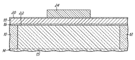
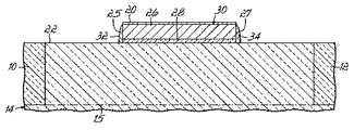
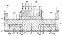
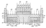
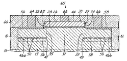
14:基板
15:井戸(ウェル)
16:ゲート誘電体層
18:ゲート導電体層
20:ハードマスク層
22:基板14の上表面
24:レジスト層
25、27:ゲート電極26の側壁
26:ゲート電極
28:ゲート誘電体
30:ゲート構造部
32、34:側壁スペーサ
35、39:接合部(界面)
36:ソース領域
37:チャネル領域
38:ドレイン領域
40:注入マスク
42、48:イオン(一方向矢印)
44:ゲート電極26の上表面
46a、46b、52a、52b、54a、54b:結晶損傷層
47、49:結晶損傷層の端部
50、53、55:ボイド
56、58:導電層
60:誘電体層
62、64、66:コンタクト
65:デバイス構造体
Claims (24)
- 上表面を有する半導体材料の基板の内部に形成されるデバイス構造体であって、
前記基板の前記半導体材料内に画定された、第1導電型の第1ドープ領域と、
前記基板の前記半導体材料内に画定された、前記第1導電型の第2ドープ領域と、
前記基板の前記半導体材料内の、前記第1ドープ領域と前記第2ドープ領域の間に配置された第3ドープ領域であって、該第3ドープ領域の前記半導体材料は前記第1導電型とは逆の第2導電型を有する、第3ドープ領域と、
前記基板の前記上表面の上にあり、前記第3ドープ領域と垂直方向に重なる関係にあるゲート構造部と、
前記基板の前記半導体材料の内部にある、前記基板の前記半導体材料によって取り囲まれた第1の複数のボイドを含んだ第1結晶損傷層と、
を備え、
前記第1ドープ領域の少なくとも一部分は、垂直方向で前記第1結晶損傷層と前記基板の前記上表面との間に配置され、前記第1結晶損傷層は前記ゲート構造部の下方を横方向に有意な距離は延びない、
デバイス構造体。 - 前記第1の複数のボイドの少なくとも一部は不活性気体を含む、請求項1に記載のデバイス構造体。
- 前記第2導電型はp型の導電性であり、従って前記第3ドープ領域内の前記半導体材料はp型導電性を有し、前記第1結晶損傷層は圧縮性応力を前記第3ドープ領域に効果的に伝達する、請求項1に記載のデバイス構造体。
- 前記第3ドープ領域は前記第1ドープ領域に並置されて前記第1ドープ領域と界面に沿って交わり、前記第1結晶損傷層は前記界面の垂直部分に概ね垂直に位置合せされた関係を有する、請求項1に記載のデバイス構造体。
- 前記第1ドープ領域は電界効果トランジスタのドレインであり、前記第2ドープ領域は前記電界効果トランジスタのソースであり、前記ゲート構造部は、ゲート電極と、該ゲート電極を前記基板の前記上表面から分離するゲート誘電体層とを含む、請求項1に記載のデバイス構造体。
- 前記第1結晶損傷層は、前記第1ドープ領域の境界内に含まれる深さに配置され、
前記基板の前記半導体材料の内部の第2結晶損傷層をさらに含み、
前記第2結晶損傷層は、前記基板の前記半導体材料により取り囲まれた第2の複数のボイドを含み、前記第1ドープ領域は、垂直方向で前記第2結晶損傷層と前記上表面との間に配置される、請求項1に記載のデバイス構造体。 - 前記第2結晶損傷層は、前記ゲート構造部の下方を横方向に有意な距離は延びない、請求項6に記載のデバイス構造体。
- 前記第1ドープ領域は垂直方向で前記第1結晶損傷層と前記上表面との間に配置される、請求項1に記載のデバイス構造体。
- 前記基板の前記半導体材料の内部の第2結晶損傷層をさらに含み、
前記第2結晶損傷層は、前記基板の前記半導体材料により取り囲まれた第2の複数のボイドを含み、前記第2ドープ領域の少なくとも一部分は垂直方向で前記第2結晶損傷層と前記基板の前記上表面との間に配置される、
請求項1に記載のデバイス構造体。 - 前記第2結晶損傷層は、前記第3ドープ領域の一部分によって前記第1結晶損傷層から分離され、前記第1結晶損傷層と前記第2結晶損傷層は不連続となる、請求項9に記載のデバイス構造体。
- 前記第2結晶損傷層は、前記ゲート構造部の下方を横方向に有意な距離は延びない、請求項9に記載のデバイス構造体。
- 前記第1結晶損傷層は、前記基板を通り抜けるイオン化放射により生成する電荷キャリアを収集し、それにより前記第1ドープ領域への前記電荷キャリアの移動を効果的に防ぐ再結合中心を含む、請求項1に記載のデバイス構造体。
- 前記ゲート構造部は第1側壁を含み、前記第1結晶損傷層は、前記ゲート構造部の前記第1側壁に概ね垂直に位置合せされて配置された端部において終る、請求項1に記載のデバイス構造体。
- 前記ゲート構造部は前記第1側壁と対向する第2側壁を有し、
前記基板の前記半導体材料の内部の第2結晶損傷層をさらに含み、
前記第2結晶損傷層は、前記基板の前記半導体材料により取り囲まれた第2の複数のボイドを含み、前記第2結晶損傷層は、垂直方向で前記第2ドープ領域の少なくとも一部分と前記基板の前記上表面との間に配置され、前記第2結晶損傷層は、前記ゲート構造部の前記第2側壁に概ね垂直に位置合せされて配置された終端部を有する、
請求項13に記載のデバイス構造体。 - 前記第2結晶損傷層は、前記第3ドープ領域の一部分によって前記第1結晶損傷層から分離され、前記第1結晶損傷層と前記第2結晶損傷層は不連続となる、請求項14に記載のデバイス構造体。
- 前記第1ドープ領域と前記第3ドープ領域はp−n接合部に沿って交わり、前記第1結晶損傷層の前記端部は前記p−n接合部に概ね横方向に位置合せされる、請求項13に記載のデバイス構造体。
- 半導体材料で構成される基板の内部にデバイス構造体を製造する方法であって、
前記基板の前記半導体材料内に第1導電型の第1ドープ領域を形成するステップと、
前記半導体材料内の前記第1導電型の第2ドープ領域であって、前記第1導電型とは逆の第2導電型を有する第3ドープ領域によって前記第1ドープ領域から横方向に分離される、前記第2ドープ領域を形成するステップと、
前記基板の上表面の上にある、前記第3ドープ領域と垂直方向に重なる関係を有するゲート構造部を形成するステップと、
前記基板の前記半導体材料によって取り囲まれた第1の複数のボイドを形成して第1結晶損傷層を画定するステップと
を含み、
前記第1結晶損傷層は、前記第1ドープ領域の少なくとも一部分により前記上表面から分離され、前記第3ドープ領域内に横方向に有意な距離は延びない、
方法。 - 前記第1の複数のボイドを形成するステップは、
不活性気体の第1の複数のイオンを、第1運動エネルギーにおいて第1ドーズ量で前記基板内に注入するステップと、
前記基板をアニールして前記第1の複数のイオンにより前記半導体材料内に生成された点欠陥を前記第1の複数のボイド内に凝集させるステップと
をさらに含む、請求項17に記載の方法。 - 前記注入された第1の複数のイオンからの前記不活性気体の原子は、前記点欠陥と共に前記第1の複数のボイド内に凝集され、その結果前記第1の複数のボイドの少なくとも一部は前記不活性気体の1つ又は複数の原子を含む、請求項18に記載の方法。
- 前記ゲート構造部は前記基板の前記上表面の上に形成され、
前記ゲート構造部及び前記上表面の上にレジスト層を塗布するステップと、
前記レジスト層をパターン付けして前記第1ドープ領域の上にある前記上表面の第1領域を露出させるステップと、
前記不活性気体の前記第1の複数のイオンの注入の間、前記ゲート構造部および前記レジスト層を、前記第3ドープ領域を覆う注入マスクとして用いて、前記第1結晶損傷層の終端部を前記ゲート構造部の第1側壁と垂直方向において概ね位置合せするステップと
をさらに含む、
請求項18に記載の方法。 - 前記注入マスクを用いて、前記不活性気体の第2の複数のイオンを、第1運動エネルギーとは異なる第2運動エネルギーにおいて第2ドーズ量で前記基板内に注入して第2の複数のボイドを形成し第2結晶損傷層を画定するステップをさらに含み、
前記第2結晶損傷層は、前記ゲート構造部の前記第1側壁と垂直方向において概ね位置合せされた端部を有し、前記第1ドープ領域の少なくとも一部分によって前記基板の前記上表面から分離される、
請求項20に記載の方法。 - 前記レジスト層は、前記第2ドープ領域の上にある前記上表面の第2領域を露出させるようにパターン付けされ、
前記不活性気体の前記第1の複数のイオンの一部が前記上表面の前記第2領域を通して前記第2ドープ領域に浸透することを可能にして、第2の複数のボイドを形成し第2結晶損傷層を画定するステップをさらに含み、
前記第2結晶損傷層は、前記ゲート構造部の第2側壁に概ね位置合せされた終端部を有し、前記第3ドープ領域によって前記第1結晶損傷層から横方向に分離される、
請求項20に記載の方法。 - 前記第1導電型の前記第1ドープ領域を形成するステップは、
前記注入マスクを用いて、不純物種の複数のイオンを前記基板の前記半導体材料の内部に注入し、前記基板の前記半導体材料をドープして前記第1ドープ領域にするステップをさらに含む、
請求項20に記載の方法。 - 前記第1ドープ領域と前記第3ドープ領域は界面に沿って交わり、前記第1結晶損傷層は前記界面に概ね位置合せされた終端部を有する、請求項17に記載の方法。
Applications Claiming Priority (2)
| Application Number | Priority Date | Filing Date | Title |
|---|---|---|---|
| US12/178,766 US7795679B2 (en) | 2008-07-24 | 2008-07-24 | Device structures with a self-aligned damage layer and methods for forming such device structures |
| US12/178766 | 2008-07-24 |
Related Child Applications (1)
| Application Number | Title | Priority Date | Filing Date |
|---|---|---|---|
| JP2011001856A Division JP5385926B2 (ja) | 2008-07-24 | 2011-01-07 | 自己整合損傷層を有するデバイス構造体の形成方法 |
Publications (2)
| Publication Number | Publication Date |
|---|---|
| JP2010034488A true JP2010034488A (ja) | 2010-02-12 |
| JP4782821B2 JP4782821B2 (ja) | 2011-09-28 |
Family
ID=40578806
Family Applications (2)
| Application Number | Title | Priority Date | Filing Date |
|---|---|---|---|
| JP2008287315A Expired - Fee Related JP4782821B2 (ja) | 2008-07-24 | 2008-11-10 | 自己整合損傷層を有するデバイス構造体 |
| JP2011001856A Expired - Fee Related JP5385926B2 (ja) | 2008-07-24 | 2011-01-07 | 自己整合損傷層を有するデバイス構造体の形成方法 |
Family Applications After (1)
| Application Number | Title | Priority Date | Filing Date |
|---|---|---|---|
| JP2011001856A Expired - Fee Related JP5385926B2 (ja) | 2008-07-24 | 2011-01-07 | 自己整合損傷層を有するデバイス構造体の形成方法 |
Country Status (5)
| Country | Link |
|---|---|
| US (1) | US7795679B2 (ja) |
| EP (1) | EP2148372B1 (ja) |
| JP (2) | JP4782821B2 (ja) |
| CN (1) | CN101635312B (ja) |
| AT (1) | ATE514189T1 (ja) |
Cited By (1)
| Publication number | Priority date | Publication date | Assignee | Title |
|---|---|---|---|---|
| JP2014056881A (ja) * | 2012-09-11 | 2014-03-27 | Mitsubishi Electric Corp | 半導体装置および半導体装置の製造方法 |
Families Citing this family (16)
| Publication number | Priority date | Publication date | Assignee | Title |
|---|---|---|---|---|
| CN102005414B (zh) * | 2009-08-28 | 2012-12-12 | 中芯国际集成电路制造(上海)有限公司 | Cmos图像传感器像素、制造方法及图像捕获设备 |
| US10128115B2 (en) * | 2010-02-26 | 2018-11-13 | Taiwan Semiconductor Manufacturing Company, Ltd. | Method of forming ultra-shallow junctions in semiconductor devices |
| CN102468164B (zh) * | 2010-10-29 | 2014-10-08 | 中国科学院微电子研究所 | 晶体管及其制造方法 |
| US9721853B2 (en) * | 2013-03-13 | 2017-08-01 | Taiwan Semiconductor Manufacturing Company, Ltd. | System and method for forming a semiconductor device |
| CN105448913A (zh) * | 2014-06-23 | 2016-03-30 | 中芯国际集成电路制造(上海)有限公司 | Cmos器件及其形成方法 |
| US10573627B2 (en) | 2015-01-09 | 2020-02-25 | Silicon Genesis Corporation | Three dimensional integrated circuit |
| US10833175B2 (en) * | 2015-06-04 | 2020-11-10 | International Business Machines Corporation | Formation of dislocation-free SiGe finFET using porous silicon |
| CN106486376A (zh) * | 2015-08-31 | 2017-03-08 | 中芯国际集成电路制造(上海)有限公司 | 鳍式场效应管及其制作方法 |
| JP6611532B2 (ja) * | 2015-09-17 | 2019-11-27 | ローム株式会社 | 半導体装置および半導体装置の製造方法 |
| CN107492487B (zh) * | 2016-06-13 | 2020-03-10 | 中芯国际集成电路制造(上海)有限公司 | 半导体器件的形成方法 |
| WO2019108945A1 (en) * | 2017-12-01 | 2019-06-06 | Silicon Genesis Corporation | Three dimensional integrated circuit |
| US11133227B2 (en) * | 2018-12-20 | 2021-09-28 | Xia Tai Xin Semiconductor (Qing Dao) Ltd. | Semiconductor device having active region and method for fabricating the same |
| US11164867B2 (en) * | 2019-08-07 | 2021-11-02 | Globalfoundries U.S. Inc. | Fin-type field-effect transistors over one or more buried polycrystalline layers |
| US11315825B2 (en) | 2019-08-28 | 2022-04-26 | Globalfoundries U.S. Inc. | Semiconductor structures including stacked depleted and high resistivity regions |
| US10971633B2 (en) * | 2019-09-04 | 2021-04-06 | Stmicroelectronics (Rousset) Sas | Structure and method of forming a semiconductor device |
| US11860417B2 (en) * | 2019-09-09 | 2024-01-02 | Cisco Technology, Inc. | Precision spacing control for optical waveguides |
Citations (8)
| Publication number | Priority date | Publication date | Assignee | Title |
|---|---|---|---|---|
| JPH0845869A (ja) * | 1994-07-25 | 1996-02-16 | Consorzio Per La Ric Sulla Microelettronica Nel Mezzogiorno | 特に集積化された電子装置における電荷キャリアの寿命の局所化される短縮のための処理、および電荷キャリアの寿命の局所化される短縮を伴う集積化された電子装置 |
| JPH1167682A (ja) * | 1997-08-08 | 1999-03-09 | Mitsubishi Electric Corp | 半導体装置の製造方法 |
| JP2000012547A (ja) * | 1998-06-26 | 2000-01-14 | Nec Corp | 半導体装置およびその製造方法 |
| US6362082B1 (en) * | 1999-06-28 | 2002-03-26 | Intel Corporation | Methodology for control of short channel effects in MOS transistors |
| US20040014304A1 (en) * | 2002-07-18 | 2004-01-22 | Micron Technology, Inc. | Stable PD-SOI devices and methods |
| US20040166624A1 (en) * | 2003-02-21 | 2004-08-26 | International Business Machines Corporation | Cmos performance enhancement using localized voids and extended defects |
| WO2006078740A2 (en) * | 2005-01-19 | 2006-07-27 | International Business Machines Corporation | Structure and method to optimize strain in cmosfets |
| US7282414B2 (en) * | 2004-05-18 | 2007-10-16 | Industrial Technology Research Institute | Fabrication methods for compressive strained-silicon and transistors using the same |
Family Cites Families (6)
| Publication number | Priority date | Publication date | Assignee | Title |
|---|---|---|---|---|
| US4766482A (en) | 1986-12-09 | 1988-08-23 | General Electric Company | Semiconductor device and method of making the same |
| US6228694B1 (en) * | 1999-06-28 | 2001-05-08 | Intel Corporation | Method of increasing the mobility of MOS transistors by use of localized stress regions |
| KR20040007025A (ko) * | 2002-07-16 | 2004-01-24 | 주식회사 하이닉스반도체 | 반도체 웨이퍼 제조 방법 |
| US7022544B2 (en) | 2002-12-18 | 2006-04-04 | International Business Machines Corporation | High speed photodiode with a barrier layer for blocking or eliminating slow photonic carriers and method for forming same |
| KR20070069160A (ko) | 2004-10-29 | 2007-07-02 | 어드밴스드 마이크로 디바이시즈, 인코포레이티드 | 서로 다른 스트레인드 채널 영역들을 갖는 반도체 영역들을포함하는 반도체 디바이스 및 이를 제조하는 방법 |
| US20070158779A1 (en) | 2006-01-12 | 2007-07-12 | International Business Machines Corporation | Methods and semiconductor structures for latch-up suppression using a buried damage layer |
-
2008
- 2008-07-24 US US12/178,766 patent/US7795679B2/en not_active Expired - Fee Related
- 2008-10-21 AT AT08167167T patent/ATE514189T1/de not_active IP Right Cessation
- 2008-10-21 EP EP08167167A patent/EP2148372B1/en not_active Not-in-force
- 2008-11-10 JP JP2008287315A patent/JP4782821B2/ja not_active Expired - Fee Related
-
2009
- 2009-07-24 CN CN2009101601442A patent/CN101635312B/zh not_active Expired - Fee Related
-
2011
- 2011-01-07 JP JP2011001856A patent/JP5385926B2/ja not_active Expired - Fee Related
Patent Citations (8)
| Publication number | Priority date | Publication date | Assignee | Title |
|---|---|---|---|---|
| JPH0845869A (ja) * | 1994-07-25 | 1996-02-16 | Consorzio Per La Ric Sulla Microelettronica Nel Mezzogiorno | 特に集積化された電子装置における電荷キャリアの寿命の局所化される短縮のための処理、および電荷キャリアの寿命の局所化される短縮を伴う集積化された電子装置 |
| JPH1167682A (ja) * | 1997-08-08 | 1999-03-09 | Mitsubishi Electric Corp | 半導体装置の製造方法 |
| JP2000012547A (ja) * | 1998-06-26 | 2000-01-14 | Nec Corp | 半導体装置およびその製造方法 |
| US6362082B1 (en) * | 1999-06-28 | 2002-03-26 | Intel Corporation | Methodology for control of short channel effects in MOS transistors |
| US20040014304A1 (en) * | 2002-07-18 | 2004-01-22 | Micron Technology, Inc. | Stable PD-SOI devices and methods |
| US20040166624A1 (en) * | 2003-02-21 | 2004-08-26 | International Business Machines Corporation | Cmos performance enhancement using localized voids and extended defects |
| US7282414B2 (en) * | 2004-05-18 | 2007-10-16 | Industrial Technology Research Institute | Fabrication methods for compressive strained-silicon and transistors using the same |
| WO2006078740A2 (en) * | 2005-01-19 | 2006-07-27 | International Business Machines Corporation | Structure and method to optimize strain in cmosfets |
Cited By (1)
| Publication number | Priority date | Publication date | Assignee | Title |
|---|---|---|---|---|
| JP2014056881A (ja) * | 2012-09-11 | 2014-03-27 | Mitsubishi Electric Corp | 半導体装置および半導体装置の製造方法 |
Also Published As
| Publication number | Publication date |
|---|---|
| EP2148372A1 (en) | 2010-01-27 |
| ATE514189T1 (de) | 2011-07-15 |
| JP4782821B2 (ja) | 2011-09-28 |
| CN101635312A (zh) | 2010-01-27 |
| CN101635312B (zh) | 2012-05-16 |
| US20100019330A1 (en) | 2010-01-28 |
| JP5385926B2 (ja) | 2014-01-08 |
| JP2011097082A (ja) | 2011-05-12 |
| US7795679B2 (en) | 2010-09-14 |
| EP2148372B1 (en) | 2011-06-22 |
Similar Documents
| Publication | Publication Date | Title |
|---|---|---|
| JP4782821B2 (ja) | 自己整合損傷層を有するデバイス構造体 | |
| CN1307709C (zh) | 具有硅锗栅极的半导体器件及其制作方法 | |
| US8513106B2 (en) | Pseudo butted junction structure for back plane connection | |
| US8466030B2 (en) | Semiconductor device and fabricating method thereof | |
| CN104217955B (zh) | N型晶体管及其制作方法、互补金属氧化物半导体 | |
| WO2013139064A1 (zh) | 一种半导体结构及其制造方法 | |
| KR100596444B1 (ko) | 반도체 소자 및 그의 제조방법 | |
| CN108573873A (zh) | 半导体器件的制造方法 | |
| WO2013139063A1 (zh) | 一种半导体结构及其制造方法 | |
| JP2012028562A (ja) | 半導体装置の製造方法 | |
| US20140021552A1 (en) | Strain Adjustment in the Formation of MOS Devices | |
| CN109427681B (zh) | 半导体结构及其形成方法 | |
| CN118231430A (zh) | 一种图像传感器及其制作方法 | |
| WO2016168994A1 (zh) | 隧穿晶体管及隧穿晶体管的制备方法 | |
| US20050153498A1 (en) | Method of manufacturing p-channel MOS transistor and CMOS transistor | |
| JP2005026661A (ja) | リフレッシュタイムを改善させた半導体素子の製造方法 | |
| US7402478B2 (en) | Method of fabricating dual gate electrode of CMOS semiconductor device | |
| US6624014B2 (en) | Process for fabricating a deep submicron complementary metal oxide semiconductor device having ultra shallow junctions | |
| KR100591172B1 (ko) | 모스 트랜지스터의 제조 방법 | |
| KR100247816B1 (ko) | 반도체장치의 제조방법 | |
| JP2012038749A (ja) | 半導体装置およびその製造方法 | |
| JP2008235567A (ja) | 半導体装置の製造方法および半導体装置 | |
| JP2004214440A (ja) | 半導体装置の製造方法 | |
| CN110571154A (zh) | 半导体器件的制造方法 | |
| KR20060019367A (ko) | 보이드가 없는 게이트 전극을 구비한 mos 트랜지스터의제조방법 |
Legal Events
| Date | Code | Title | Description |
|---|---|---|---|
| A521 | Request for written amendment filed |
Free format text: JAPANESE INTERMEDIATE CODE: A523 Effective date: 20091225 |
|
| A131 | Notification of reasons for refusal |
Free format text: JAPANESE INTERMEDIATE CODE: A131 Effective date: 20100406 |
|
| A521 | Request for written amendment filed |
Free format text: JAPANESE INTERMEDIATE CODE: A523 Effective date: 20100616 |
|
| A02 | Decision of refusal |
Free format text: JAPANESE INTERMEDIATE CODE: A02 Effective date: 20100914 |
|
| A521 | Request for written amendment filed |
Free format text: JAPANESE INTERMEDIATE CODE: A523 Effective date: 20110107 |
|
| A911 | Transfer to examiner for re-examination before appeal (zenchi) |
Free format text: JAPANESE INTERMEDIATE CODE: A911 Effective date: 20110117 |
|
| A131 | Notification of reasons for refusal |
Free format text: JAPANESE INTERMEDIATE CODE: A131 Effective date: 20110531 |
|
| A521 | Request for written amendment filed |
Free format text: JAPANESE INTERMEDIATE CODE: A523 Effective date: 20110601 |
|
| TRDD | Decision of grant or rejection written | ||
| A01 | Written decision to grant a patent or to grant a registration (utility model) |
Free format text: JAPANESE INTERMEDIATE CODE: A01 Effective date: 20110621 |
|
| RD14 | Notification of resignation of power of sub attorney |
Free format text: JAPANESE INTERMEDIATE CODE: A7434 Effective date: 20110621 |
|
| A01 | Written decision to grant a patent or to grant a registration (utility model) |
Free format text: JAPANESE INTERMEDIATE CODE: A01 |
|
| A61 | First payment of annual fees (during grant procedure) |
Free format text: JAPANESE INTERMEDIATE CODE: A61 Effective date: 20110707 |
|
| FPAY | Renewal fee payment (event date is renewal date of database) |
Free format text: PAYMENT UNTIL: 20140715 Year of fee payment: 3 |
|
| R150 | Certificate of patent or registration of utility model |
Free format text: JAPANESE INTERMEDIATE CODE: R150 |
|
| LAPS | Cancellation because of no payment of annual fees |