JP2010026368A - 液晶表示装置 - Google Patents
液晶表示装置 Download PDFInfo
- Publication number
- JP2010026368A JP2010026368A JP2008189604A JP2008189604A JP2010026368A JP 2010026368 A JP2010026368 A JP 2010026368A JP 2008189604 A JP2008189604 A JP 2008189604A JP 2008189604 A JP2008189604 A JP 2008189604A JP 2010026368 A JP2010026368 A JP 2010026368A
- Authority
- JP
- Japan
- Prior art keywords
- color filter
- liquid crystal
- light shielding
- shielding film
- film
- Prior art date
- Legal status (The legal status is an assumption and is not a legal conclusion. Google has not performed a legal analysis and makes no representation as to the accuracy of the status listed.)
- Granted
Links
- 239000004973 liquid crystal related substance Substances 0.000 title claims abstract description 76
- 239000000758 substrate Substances 0.000 claims abstract description 109
- 239000003566 sealing material Substances 0.000 claims abstract description 42
- 239000011159 matrix material Substances 0.000 claims description 6
- 238000007650 screen-printing Methods 0.000 abstract description 29
- 239000010408 film Substances 0.000 description 158
- 238000002161 passivation Methods 0.000 description 15
- 210000002858 crystal cell Anatomy 0.000 description 8
- 238000000034 method Methods 0.000 description 7
- 229910045601 alloy Inorganic materials 0.000 description 5
- 239000000956 alloy Substances 0.000 description 5
- 229910021417 amorphous silicon Inorganic materials 0.000 description 5
- 238000004519 manufacturing process Methods 0.000 description 5
- 230000015572 biosynthetic process Effects 0.000 description 4
- 238000010586 diagram Methods 0.000 description 4
- 238000004544 sputter deposition Methods 0.000 description 4
- 229910015202 MoCr Inorganic materials 0.000 description 3
- 238000005530 etching Methods 0.000 description 3
- 229910052751 metal Inorganic materials 0.000 description 3
- 239000002184 metal Substances 0.000 description 3
- 239000011347 resin Substances 0.000 description 3
- 229920005989 resin Polymers 0.000 description 3
- 239000004065 semiconductor Substances 0.000 description 3
- 239000004925 Acrylic resin Substances 0.000 description 2
- 229920000178 Acrylic resin Polymers 0.000 description 2
- 230000005540 biological transmission Effects 0.000 description 2
- 230000000694 effects Effects 0.000 description 2
- 238000002347 injection Methods 0.000 description 2
- 239000007924 injection Substances 0.000 description 2
- 238000005498 polishing Methods 0.000 description 2
- VYZAMTAEIAYCRO-UHFFFAOYSA-N Chromium Chemical compound [Cr] VYZAMTAEIAYCRO-UHFFFAOYSA-N 0.000 description 1
- XUIMIQQOPSSXEZ-UHFFFAOYSA-N Silicon Chemical compound [Si] XUIMIQQOPSSXEZ-UHFFFAOYSA-N 0.000 description 1
- 238000003490 calendering Methods 0.000 description 1
- 229910052804 chromium Inorganic materials 0.000 description 1
- 239000011651 chromium Substances 0.000 description 1
- 238000011109 contamination Methods 0.000 description 1
- 239000003822 epoxy resin Substances 0.000 description 1
- 238000002474 experimental method Methods 0.000 description 1
- 239000011521 glass Substances 0.000 description 1
- 239000012535 impurity Substances 0.000 description 1
- AMGQUBHHOARCQH-UHFFFAOYSA-N indium;oxotin Chemical compound [In].[Sn]=O AMGQUBHHOARCQH-UHFFFAOYSA-N 0.000 description 1
- 239000007788 liquid Substances 0.000 description 1
- 239000000463 material Substances 0.000 description 1
- 238000000059 patterning Methods 0.000 description 1
- 229920002120 photoresistant polymer Polymers 0.000 description 1
- 239000000049 pigment Substances 0.000 description 1
- 238000005268 plasma chemical vapour deposition Methods 0.000 description 1
- 229920000647 polyepoxide Polymers 0.000 description 1
- 229920001721 polyimide Polymers 0.000 description 1
- 239000009719 polyimide resin Substances 0.000 description 1
- 238000007639 printing Methods 0.000 description 1
- 229910052710 silicon Inorganic materials 0.000 description 1
- 239000010703 silicon Substances 0.000 description 1
- 125000006850 spacer group Chemical group 0.000 description 1
- 239000010935 stainless steel Substances 0.000 description 1
- 229910001220 stainless steel Inorganic materials 0.000 description 1
- 229920001187 thermosetting polymer Polymers 0.000 description 1
- 239000010409 thin film Substances 0.000 description 1
- 238000002834 transmittance Methods 0.000 description 1
Images


Classifications
-
- G—PHYSICS
- G02—OPTICS
- G02F—OPTICAL DEVICES OR ARRANGEMENTS FOR THE CONTROL OF LIGHT BY MODIFICATION OF THE OPTICAL PROPERTIES OF THE MEDIA OF THE ELEMENTS INVOLVED THEREIN; NON-LINEAR OPTICS; FREQUENCY-CHANGING OF LIGHT; OPTICAL LOGIC ELEMENTS; OPTICAL ANALOGUE/DIGITAL CONVERTERS
- G02F1/00—Devices or arrangements for the control of the intensity, colour, phase, polarisation or direction of light arriving from an independent light source, e.g. switching, gating or modulating; Non-linear optics
- G02F1/01—Devices or arrangements for the control of the intensity, colour, phase, polarisation or direction of light arriving from an independent light source, e.g. switching, gating or modulating; Non-linear optics for the control of the intensity, phase, polarisation or colour
- G02F1/13—Devices or arrangements for the control of the intensity, colour, phase, polarisation or direction of light arriving from an independent light source, e.g. switching, gating or modulating; Non-linear optics for the control of the intensity, phase, polarisation or colour based on liquid crystals, e.g. single liquid crystal display cells
- G02F1/133—Constructional arrangements; Operation of liquid crystal cells; Circuit arrangements
- G02F1/1333—Constructional arrangements; Manufacturing methods
- G02F1/1335—Structural association of cells with optical devices, e.g. polarisers or reflectors
- G02F1/133509—Filters, e.g. light shielding masks
- G02F1/133514—Colour filters
-
- G—PHYSICS
- G02—OPTICS
- G02F—OPTICAL DEVICES OR ARRANGEMENTS FOR THE CONTROL OF LIGHT BY MODIFICATION OF THE OPTICAL PROPERTIES OF THE MEDIA OF THE ELEMENTS INVOLVED THEREIN; NON-LINEAR OPTICS; FREQUENCY-CHANGING OF LIGHT; OPTICAL LOGIC ELEMENTS; OPTICAL ANALOGUE/DIGITAL CONVERTERS
- G02F1/00—Devices or arrangements for the control of the intensity, colour, phase, polarisation or direction of light arriving from an independent light source, e.g. switching, gating or modulating; Non-linear optics
- G02F1/01—Devices or arrangements for the control of the intensity, colour, phase, polarisation or direction of light arriving from an independent light source, e.g. switching, gating or modulating; Non-linear optics for the control of the intensity, phase, polarisation or colour
- G02F1/13—Devices or arrangements for the control of the intensity, colour, phase, polarisation or direction of light arriving from an independent light source, e.g. switching, gating or modulating; Non-linear optics for the control of the intensity, phase, polarisation or colour based on liquid crystals, e.g. single liquid crystal display cells
- G02F1/133—Constructional arrangements; Operation of liquid crystal cells; Circuit arrangements
- G02F1/1333—Constructional arrangements; Manufacturing methods
- G02F1/1339—Gaskets; Spacers; Sealing of cells
-
- G—PHYSICS
- G02—OPTICS
- G02F—OPTICAL DEVICES OR ARRANGEMENTS FOR THE CONTROL OF LIGHT BY MODIFICATION OF THE OPTICAL PROPERTIES OF THE MEDIA OF THE ELEMENTS INVOLVED THEREIN; NON-LINEAR OPTICS; FREQUENCY-CHANGING OF LIGHT; OPTICAL LOGIC ELEMENTS; OPTICAL ANALOGUE/DIGITAL CONVERTERS
- G02F1/00—Devices or arrangements for the control of the intensity, colour, phase, polarisation or direction of light arriving from an independent light source, e.g. switching, gating or modulating; Non-linear optics
- G02F1/01—Devices or arrangements for the control of the intensity, colour, phase, polarisation or direction of light arriving from an independent light source, e.g. switching, gating or modulating; Non-linear optics for the control of the intensity, phase, polarisation or colour
- G02F1/13—Devices or arrangements for the control of the intensity, colour, phase, polarisation or direction of light arriving from an independent light source, e.g. switching, gating or modulating; Non-linear optics for the control of the intensity, phase, polarisation or colour based on liquid crystals, e.g. single liquid crystal display cells
- G02F1/133—Constructional arrangements; Operation of liquid crystal cells; Circuit arrangements
- G02F1/1333—Constructional arrangements; Manufacturing methods
- G02F1/1335—Structural association of cells with optical devices, e.g. polarisers or reflectors
- G02F1/133509—Filters, e.g. light shielding masks
- G02F1/133512—Light shielding layers, e.g. black matrix
-
- G—PHYSICS
- G02—OPTICS
- G02F—OPTICAL DEVICES OR ARRANGEMENTS FOR THE CONTROL OF LIGHT BY MODIFICATION OF THE OPTICAL PROPERTIES OF THE MEDIA OF THE ELEMENTS INVOLVED THEREIN; NON-LINEAR OPTICS; FREQUENCY-CHANGING OF LIGHT; OPTICAL LOGIC ELEMENTS; OPTICAL ANALOGUE/DIGITAL CONVERTERS
- G02F1/00—Devices or arrangements for the control of the intensity, colour, phase, polarisation or direction of light arriving from an independent light source, e.g. switching, gating or modulating; Non-linear optics
- G02F1/01—Devices or arrangements for the control of the intensity, colour, phase, polarisation or direction of light arriving from an independent light source, e.g. switching, gating or modulating; Non-linear optics for the control of the intensity, phase, polarisation or colour
- G02F1/13—Devices or arrangements for the control of the intensity, colour, phase, polarisation or direction of light arriving from an independent light source, e.g. switching, gating or modulating; Non-linear optics for the control of the intensity, phase, polarisation or colour based on liquid crystals, e.g. single liquid crystal display cells
- G02F1/133—Constructional arrangements; Operation of liquid crystal cells; Circuit arrangements
- G02F1/1333—Constructional arrangements; Manufacturing methods
- G02F1/1335—Structural association of cells with optical devices, e.g. polarisers or reflectors
- G02F1/133509—Filters, e.g. light shielding masks
- G02F1/133514—Colour filters
- G02F1/133519—Overcoatings
-
- G—PHYSICS
- G02—OPTICS
- G02F—OPTICAL DEVICES OR ARRANGEMENTS FOR THE CONTROL OF LIGHT BY MODIFICATION OF THE OPTICAL PROPERTIES OF THE MEDIA OF THE ELEMENTS INVOLVED THEREIN; NON-LINEAR OPTICS; FREQUENCY-CHANGING OF LIGHT; OPTICAL LOGIC ELEMENTS; OPTICAL ANALOGUE/DIGITAL CONVERTERS
- G02F1/00—Devices or arrangements for the control of the intensity, colour, phase, polarisation or direction of light arriving from an independent light source, e.g. switching, gating or modulating; Non-linear optics
- G02F1/01—Devices or arrangements for the control of the intensity, colour, phase, polarisation or direction of light arriving from an independent light source, e.g. switching, gating or modulating; Non-linear optics for the control of the intensity, phase, polarisation or colour
- G02F1/13—Devices or arrangements for the control of the intensity, colour, phase, polarisation or direction of light arriving from an independent light source, e.g. switching, gating or modulating; Non-linear optics for the control of the intensity, phase, polarisation or colour based on liquid crystals, e.g. single liquid crystal display cells
- G02F1/133—Constructional arrangements; Operation of liquid crystal cells; Circuit arrangements
- G02F1/1333—Constructional arrangements; Manufacturing methods
- G02F1/1337—Surface-induced orientation of the liquid crystal molecules, e.g. by alignment layers
Abstract
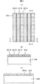
【解決手段】遮光膜202が横方向に延在し、縦方向に配列している。赤カラーフィルタ201R、青カラーフィルタ201B、緑カラーフィルタ201Gが所定の間隔を持って縦方向に延在している。青カラーフィルタ201Bは遮光膜を覆って横方向にも延在している。赤カラーフィルタ201Rおよび緑カラーフィルタ201Gに沿った断面においては、遮光膜202の上が他の部分に比較して、青カラーフィルタ201Bと遮光膜202の厚さの分高くなっている。スクリーン印刷時、この高くなった部分がメッシュのストッパーとなるので、メッシュによるムラの発生を防止することが出来る。
【選択図】図4
Description
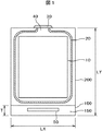
図1において、TFT基板100上に対向基板200が設置されている。TFT基板100と対向基板200の間に液晶層300が挟持されている。TFT基板100と対向基板200とは額縁部に形成されたシール材20によって接着している。TFT基板100は対向基板200よりも大きく形成されており、TFT基板100が対向基板200よりも大きくなっている部分には、液晶セル1に電源、映像信号、走査信号等を供給するための端子部150が形成されている。また、端子部150には、走査線、映像信号線等を駆動するためのICドライバ50が設置されている。
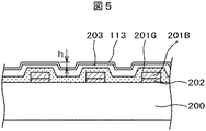
図4(a)は表示領域10の画素構造の平面図であり、図4(b)は図4(a)のA−A断面図であり、図4(c)は図4(a)のB−B断面図である。図4(a)において、赤カラーフィルタ201R、青カラーフィルタ201B、緑カラーフィルタ201Gが各々所定間隔をおいて縦方向に延在している。図4におけるカラーフィルタ201の形成順序は赤カラーフィルタ201R、青カラーフィルタ201B、緑カラーフィルタ201Gの順である。
Claims (6)
- 画素電極とTFTを含む画素がマトリクス状に形成されたTFT基板と、カラーフィルタが形成された対向基板と、前記TFT基板と前記カラーフィルタとの間に液晶が挟持され、前記TFT基板と前記対向基板とは、前記対向基板の周辺に形成されたシール材を介して接着している液晶表示装置であって、
前記対向基板には遮光膜が第1の方向に延在して第2の方向に配列し、赤カラーフィルタが第2の方向に延在して第1の方向に配列し、青カラーフィルタが第2の方向に延在して第1の方向に配列し、緑カラーフィルタが第2の方向に延在して第1の方向に配列し、
前記赤カラーフィルタ、前記青カラーフィルタ、前記緑カラーフィルタのうちの一色のカラーフィルタは、前記遮光膜を覆って第1の方向に延在し、前記一色のカラーフィルタが、前記第1の方向に延在した部分では、2層のカラーフィルタが形成されており、
前記赤カラーフィルタ、前記青カラーフィルタ、および、前記緑カラーフィルタを覆ってオーバーコート膜が形成され、前記オーバーコート膜を覆って配向膜が形成されていることを特徴とする液晶表示装置。 - 前記遮光膜上において前記2層のカラーフィルタが形成されている部分と、前記遮光膜が形成されていない部分の高さの差は、600nm以上で、1.8μm以下であることを特徴とする請求項1に記載の液晶表示装置。
- 前記液晶表示装置はIPS方式の液晶表示装置であることを特徴とする請求項1に記載の液晶表示装置。
- 画素電極とTFTを含む画素がマトリクス状に形成されたTFT基板と、カラーフィルタが形成された対向基板と、前記TFT基板と前記カラーフィルタとの間に液晶が挟持され、前記TFT基板と前記対向基板とは、前記対向基板の周辺に形成されたシール材を介して接着している液晶表示装置であって、
前記対向基板には遮光膜が第1の方向に延在して第2の方向に配列し、赤カラーフィルタが第2の方向に延在して第1の方向に配列するとともに、前記遮光膜を覆って前記第1の方向に延在して第2の方向に配列し、青カラーフィルタが第2の方向に延在して第1の方向に配列するとともに、前記遮光膜を覆って前記第1の方向に延在して第2の方向に配列し、緑カラーフィルタが第2の方向に延在して第1の方向に配列するとともに、前記遮光膜を覆って前記第1の方向に延在して第2の方向に配列し、
前記赤カラーフィルタ、前記青カラーフィルタ、および、前記緑カラーフィルタを覆ってオーバーコート膜が形成され、前記オーバーコート膜を覆って配向膜が形成されていることを特徴とする液晶表示装置。 - 前記遮光膜が形成されている部分と、前記遮光膜が形成されていない部分の高さの差は、600nm以上で、1.8μm以下であることを特徴とする請求項4に記載の液晶表示装置。
- 前記液晶表示装置はIPS方式の液晶表示装置であることを特徴とする請求項4に記載の液晶表示装置。
Priority Applications (2)
| Application Number | Priority Date | Filing Date | Title |
|---|---|---|---|
| JP2008189604A JP5156517B2 (ja) | 2008-07-23 | 2008-07-23 | 液晶表示装置 |
| US12/506,437 US8749734B2 (en) | 2008-07-23 | 2009-07-21 | Liquid crystal display device with layers of different color filters covering light shielding films |
Applications Claiming Priority (1)
| Application Number | Priority Date | Filing Date | Title |
|---|---|---|---|
| JP2008189604A JP5156517B2 (ja) | 2008-07-23 | 2008-07-23 | 液晶表示装置 |
Publications (2)
| Publication Number | Publication Date |
|---|---|
| JP2010026368A true JP2010026368A (ja) | 2010-02-04 |
| JP5156517B2 JP5156517B2 (ja) | 2013-03-06 |
Family
ID=41568332
Family Applications (1)
| Application Number | Title | Priority Date | Filing Date |
|---|---|---|---|
| JP2008189604A Active JP5156517B2 (ja) | 2008-07-23 | 2008-07-23 | 液晶表示装置 |
Country Status (2)
| Country | Link |
|---|---|
| US (1) | US8749734B2 (ja) |
| JP (1) | JP5156517B2 (ja) |
Cited By (2)
| Publication number | Priority date | Publication date | Assignee | Title |
|---|---|---|---|---|
| KR101791546B1 (ko) * | 2011-07-05 | 2017-10-31 | 삼성디스플레이 주식회사 | 표시 기판 및 이의 리페어 방법 |
| JP2019003004A (ja) * | 2017-06-14 | 2019-01-10 | 三菱電機株式会社 | 液晶表示装置 |
Families Citing this family (10)
| Publication number | Priority date | Publication date | Assignee | Title |
|---|---|---|---|---|
| JP2011053608A (ja) * | 2009-09-04 | 2011-03-17 | Mitsubishi Electric Corp | 液晶パネルの製造方法 |
| JP6605789B2 (ja) * | 2013-06-18 | 2019-11-13 | パナソニック インテレクチュアル プロパティ コーポレーション オブ アメリカ | 送信方法、受信方法、送信装置、および、受信装置 |
| CN104166273A (zh) * | 2014-06-26 | 2014-11-26 | 京东方科技集团股份有限公司 | 显示基板、显示基板母板和显示装置 |
| CN104950527A (zh) * | 2015-07-01 | 2015-09-30 | 合肥鑫晟光电科技有限公司 | 显示基板及其制造方法、显示面板和显示装置 |
| KR102408899B1 (ko) * | 2015-10-02 | 2022-06-15 | 엘지디스플레이 주식회사 | 액정표시장치 및 그의 제조 방법 |
| KR20170130660A (ko) * | 2016-05-18 | 2017-11-29 | 삼성디스플레이 주식회사 | 표시 장치 |
| JP2018124480A (ja) | 2017-02-02 | 2018-08-09 | 株式会社ジャパンディスプレイ | 表示装置 |
| CN108983479B (zh) | 2017-06-01 | 2019-11-05 | 京东方科技集团股份有限公司 | 显示基板及其制备方法和显示装置 |
| CN109116615A (zh) * | 2018-08-20 | 2019-01-01 | 深圳市华星光电技术有限公司 | 彩膜基板及液晶面板 |
| CN111413823A (zh) | 2019-01-07 | 2020-07-14 | 群创光电股份有限公司 | 电子装置 |
Citations (4)
| Publication number | Priority date | Publication date | Assignee | Title |
|---|---|---|---|---|
| JPH0664359A (ja) * | 1992-08-24 | 1994-03-08 | Matsushita Electric Ind Co Ltd | スクリーン印刷版 |
| JPH1010520A (ja) * | 1996-06-19 | 1998-01-16 | Dainippon Printing Co Ltd | 強誘電性液晶用カラーフィルタおよびこれを用いた強誘電性液晶表示装置 |
| JP2002023148A (ja) * | 2000-04-18 | 2002-01-23 | Semiconductor Energy Lab Co Ltd | 電気光学装置 |
| JP2007052360A (ja) * | 2005-08-19 | 2007-03-01 | Toshiba Matsushita Display Technology Co Ltd | カラーフィルタ基板、液晶表示パネルおよび複数のカラーフィルタ基板の製造方法 |
Family Cites Families (4)
| Publication number | Priority date | Publication date | Assignee | Title |
|---|---|---|---|---|
| US4758734A (en) * | 1984-03-13 | 1988-07-19 | Nec Corporation | High resolution image sensor array using amorphous photo-diodes |
| JPH0721562B2 (ja) * | 1987-05-14 | 1995-03-08 | 凸版印刷株式会社 | カラ−フイルタ |
| DE68920702T2 (de) * | 1988-11-10 | 1995-06-14 | Toshiba Kawasaki Kk | Flüssigkristall-Anzeigevorrichtung, Farbfilter hierfür und Verfahren zur Herstellung des Farbfilters. |
| JP2003131020A (ja) | 2001-10-26 | 2003-05-08 | Toppan Printing Co Ltd | カラーフィルタの製造方法 |
-
2008
- 2008-07-23 JP JP2008189604A patent/JP5156517B2/ja active Active
-
2009
- 2009-07-21 US US12/506,437 patent/US8749734B2/en active Active
Patent Citations (4)
| Publication number | Priority date | Publication date | Assignee | Title |
|---|---|---|---|---|
| JPH0664359A (ja) * | 1992-08-24 | 1994-03-08 | Matsushita Electric Ind Co Ltd | スクリーン印刷版 |
| JPH1010520A (ja) * | 1996-06-19 | 1998-01-16 | Dainippon Printing Co Ltd | 強誘電性液晶用カラーフィルタおよびこれを用いた強誘電性液晶表示装置 |
| JP2002023148A (ja) * | 2000-04-18 | 2002-01-23 | Semiconductor Energy Lab Co Ltd | 電気光学装置 |
| JP2007052360A (ja) * | 2005-08-19 | 2007-03-01 | Toshiba Matsushita Display Technology Co Ltd | カラーフィルタ基板、液晶表示パネルおよび複数のカラーフィルタ基板の製造方法 |
Cited By (3)
| Publication number | Priority date | Publication date | Assignee | Title |
|---|---|---|---|---|
| KR101791546B1 (ko) * | 2011-07-05 | 2017-10-31 | 삼성디스플레이 주식회사 | 표시 기판 및 이의 리페어 방법 |
| JP2019003004A (ja) * | 2017-06-14 | 2019-01-10 | 三菱電機株式会社 | 液晶表示装置 |
| JP7007817B2 (ja) | 2017-06-14 | 2022-01-25 | トライベイル テクノロジーズ, エルエルシー | 液晶表示装置 |
Also Published As
| Publication number | Publication date |
|---|---|
| US8749734B2 (en) | 2014-06-10 |
| US20100020275A1 (en) | 2010-01-28 |
| JP5156517B2 (ja) | 2013-03-06 |
Similar Documents
| Publication | Publication Date | Title |
|---|---|---|
| JP5156517B2 (ja) | 液晶表示装置 | |
| US8368864B2 (en) | Liquid crystal display device with spacer in the sealant | |
| US10473984B2 (en) | Liquid crystal display device | |
| US9417485B2 (en) | Liquid crystal display device | |
| JP5553531B2 (ja) | 液晶表示装置 | |
| US9977280B2 (en) | COT type liquid crystal display device | |
| US8421973B2 (en) | Liquid crystal display device | |
| JP5239924B2 (ja) | 液晶表示装置及びそれを用いた電子機器 | |
| JP6649788B2 (ja) | 液晶表示装置 | |
| KR20080026404A (ko) | 어레이 기판, 이를 갖는 표시패널 및 그 제조 방법 | |
| US20210088855A1 (en) | Liquid crystal display device | |
| US20110216282A1 (en) | Liquid crystal display device | |
| KR20090130938A (ko) | 표시 기판 및 이를 포함하는 표시 장치 | |
| JP2018025670A (ja) | 液晶表示装置 | |
| JP2004272012A (ja) | 表示装置 | |
| JP2017187530A (ja) | 液晶表示装置 | |
| JP4722538B2 (ja) | 表示装置 | |
| JP5275650B2 (ja) | 液晶表示装置 | |
| JP2009169162A (ja) | 液晶表示装置 | |
| KR20130018056A (ko) | 액정표시장치 | |
| US20100045914A1 (en) | Liquid crystal display device | |
| JP5492326B2 (ja) | 液晶表示装置の製造方法 | |
| JP5026883B2 (ja) | 電気光学装置、及び電子機器 | |
| JP2020013148A (ja) | 液晶表示装置 | |
| JP2009271366A (ja) | 液晶表示装置 |
Legal Events
| Date | Code | Title | Description |
|---|---|---|---|
| A711 | Notification of change in applicant |
Free format text: JAPANESE INTERMEDIATE CODE: A712 Effective date: 20110218 |
|
| RD03 | Notification of appointment of power of attorney |
Free format text: JAPANESE INTERMEDIATE CODE: A7423 Effective date: 20110218 |
|
| A621 | Written request for application examination |
Free format text: JAPANESE INTERMEDIATE CODE: A621 Effective date: 20110512 |
|
| A131 | Notification of reasons for refusal |
Free format text: JAPANESE INTERMEDIATE CODE: A131 Effective date: 20120828 |
|
| A977 | Report on retrieval |
Free format text: JAPANESE INTERMEDIATE CODE: A971007 Effective date: 20120829 |
|
| A521 | Request for written amendment filed |
Free format text: JAPANESE INTERMEDIATE CODE: A523 Effective date: 20121017 |
|
| TRDD | Decision of grant or rejection written | ||
| A01 | Written decision to grant a patent or to grant a registration (utility model) |
Free format text: JAPANESE INTERMEDIATE CODE: A01 Effective date: 20121113 |
|
| A61 | First payment of annual fees (during grant procedure) |
Free format text: JAPANESE INTERMEDIATE CODE: A61 Effective date: 20121210 |
|
| FPAY | Renewal fee payment (event date is renewal date of database) |
Free format text: PAYMENT UNTIL: 20151214 Year of fee payment: 3 |
|
| R150 | Certificate of patent or registration of utility model |
Ref document number: 5156517 Country of ref document: JP Free format text: JAPANESE INTERMEDIATE CODE: R150 Free format text: JAPANESE INTERMEDIATE CODE: R150 |
|
| R250 | Receipt of annual fees |
Free format text: JAPANESE INTERMEDIATE CODE: R250 |
|
| R250 | Receipt of annual fees |
Free format text: JAPANESE INTERMEDIATE CODE: R250 |
|
| R250 | Receipt of annual fees |
Free format text: JAPANESE INTERMEDIATE CODE: R250 |
|
| R250 | Receipt of annual fees |
Free format text: JAPANESE INTERMEDIATE CODE: R250 |
|
| R250 | Receipt of annual fees |
Free format text: JAPANESE INTERMEDIATE CODE: R250 |
|
| R250 | Receipt of annual fees |
Free format text: JAPANESE INTERMEDIATE CODE: R250 |
|
| S531 | Written request for registration of change of domicile |
Free format text: JAPANESE INTERMEDIATE CODE: R313531 |
|
| S533 | Written request for registration of change of name |
Free format text: JAPANESE INTERMEDIATE CODE: R313533 |
|
| R350 | Written notification of registration of transfer |
Free format text: JAPANESE INTERMEDIATE CODE: R350 |
|
| R250 | Receipt of annual fees |
Free format text: JAPANESE INTERMEDIATE CODE: R250 |
|
| R250 | Receipt of annual fees |
Free format text: JAPANESE INTERMEDIATE CODE: R250 |
|
| S111 | Request for change of ownership or part of ownership |
Free format text: JAPANESE INTERMEDIATE CODE: R313117 |
|
| R350 | Written notification of registration of transfer |
Free format text: JAPANESE INTERMEDIATE CODE: R350 |
|
| R250 | Receipt of annual fees |
Free format text: JAPANESE INTERMEDIATE CODE: R250 |