JP2010026368A - Liquid crystal display device - Google Patents
Liquid crystal display device Download PDFInfo
- Publication number
- JP2010026368A JP2010026368A JP2008189604A JP2008189604A JP2010026368A JP 2010026368 A JP2010026368 A JP 2010026368A JP 2008189604 A JP2008189604 A JP 2008189604A JP 2008189604 A JP2008189604 A JP 2008189604A JP 2010026368 A JP2010026368 A JP 2010026368A
- Authority
- JP
- Japan
- Prior art keywords
- color filter
- liquid crystal
- light shielding
- shielding film
- film
- Prior art date
- Legal status (The legal status is an assumption and is not a legal conclusion. Google has not performed a legal analysis and makes no representation as to the accuracy of the status listed.)
- Granted
Links
- 239000004973 liquid crystal related substance Substances 0.000 title claims abstract description 76
- 239000000758 substrate Substances 0.000 claims abstract description 109
- 239000003566 sealing material Substances 0.000 claims abstract description 42
- 239000011159 matrix material Substances 0.000 claims description 6
- 238000007650 screen-printing Methods 0.000 abstract description 29
- 239000010408 film Substances 0.000 description 158
- 238000002161 passivation Methods 0.000 description 15
- 210000002858 crystal cell Anatomy 0.000 description 8
- 238000000034 method Methods 0.000 description 7
- 229910045601 alloy Inorganic materials 0.000 description 5
- 239000000956 alloy Substances 0.000 description 5
- 229910021417 amorphous silicon Inorganic materials 0.000 description 5
- 238000004519 manufacturing process Methods 0.000 description 5
- 230000015572 biosynthetic process Effects 0.000 description 4
- 238000010586 diagram Methods 0.000 description 4
- 238000004544 sputter deposition Methods 0.000 description 4
- 229910015202 MoCr Inorganic materials 0.000 description 3
- 238000005530 etching Methods 0.000 description 3
- 229910052751 metal Inorganic materials 0.000 description 3
- 239000002184 metal Substances 0.000 description 3
- 239000011347 resin Substances 0.000 description 3
- 229920005989 resin Polymers 0.000 description 3
- 239000004065 semiconductor Substances 0.000 description 3
- 239000004925 Acrylic resin Substances 0.000 description 2
- 229920000178 Acrylic resin Polymers 0.000 description 2
- 230000005540 biological transmission Effects 0.000 description 2
- 230000000694 effects Effects 0.000 description 2
- 238000002347 injection Methods 0.000 description 2
- 239000007924 injection Substances 0.000 description 2
- 238000005498 polishing Methods 0.000 description 2
- VYZAMTAEIAYCRO-UHFFFAOYSA-N Chromium Chemical compound [Cr] VYZAMTAEIAYCRO-UHFFFAOYSA-N 0.000 description 1
- XUIMIQQOPSSXEZ-UHFFFAOYSA-N Silicon Chemical compound [Si] XUIMIQQOPSSXEZ-UHFFFAOYSA-N 0.000 description 1
- 238000003490 calendering Methods 0.000 description 1
- 229910052804 chromium Inorganic materials 0.000 description 1
- 239000011651 chromium Substances 0.000 description 1
- 238000011109 contamination Methods 0.000 description 1
- 239000003822 epoxy resin Substances 0.000 description 1
- 238000002474 experimental method Methods 0.000 description 1
- 239000011521 glass Substances 0.000 description 1
- 239000012535 impurity Substances 0.000 description 1
- AMGQUBHHOARCQH-UHFFFAOYSA-N indium;oxotin Chemical compound [In].[Sn]=O AMGQUBHHOARCQH-UHFFFAOYSA-N 0.000 description 1
- 239000007788 liquid Substances 0.000 description 1
- 239000000463 material Substances 0.000 description 1
- 238000000059 patterning Methods 0.000 description 1
- 229920002120 photoresistant polymer Polymers 0.000 description 1
- 239000000049 pigment Substances 0.000 description 1
- 238000005268 plasma chemical vapour deposition Methods 0.000 description 1
- 229920000647 polyepoxide Polymers 0.000 description 1
- 229920001721 polyimide Polymers 0.000 description 1
- 239000009719 polyimide resin Substances 0.000 description 1
- 238000007639 printing Methods 0.000 description 1
- 229910052710 silicon Inorganic materials 0.000 description 1
- 239000010703 silicon Substances 0.000 description 1
- 125000006850 spacer group Chemical group 0.000 description 1
- 239000010935 stainless steel Substances 0.000 description 1
- 229910001220 stainless steel Inorganic materials 0.000 description 1
- 229920001187 thermosetting polymer Polymers 0.000 description 1
- 239000010409 thin film Substances 0.000 description 1
- 238000002834 transmittance Methods 0.000 description 1
Images


Classifications
-
- G—PHYSICS
- G02—OPTICS
- G02F—OPTICAL DEVICES OR ARRANGEMENTS FOR THE CONTROL OF LIGHT BY MODIFICATION OF THE OPTICAL PROPERTIES OF THE MEDIA OF THE ELEMENTS INVOLVED THEREIN; NON-LINEAR OPTICS; FREQUENCY-CHANGING OF LIGHT; OPTICAL LOGIC ELEMENTS; OPTICAL ANALOGUE/DIGITAL CONVERTERS
- G02F1/00—Devices or arrangements for the control of the intensity, colour, phase, polarisation or direction of light arriving from an independent light source, e.g. switching, gating or modulating; Non-linear optics
- G02F1/01—Devices or arrangements for the control of the intensity, colour, phase, polarisation or direction of light arriving from an independent light source, e.g. switching, gating or modulating; Non-linear optics for the control of the intensity, phase, polarisation or colour
- G02F1/13—Devices or arrangements for the control of the intensity, colour, phase, polarisation or direction of light arriving from an independent light source, e.g. switching, gating or modulating; Non-linear optics for the control of the intensity, phase, polarisation or colour based on liquid crystals, e.g. single liquid crystal display cells
- G02F1/133—Constructional arrangements; Operation of liquid crystal cells; Circuit arrangements
- G02F1/1333—Constructional arrangements; Manufacturing methods
- G02F1/1335—Structural association of cells with optical devices, e.g. polarisers or reflectors
- G02F1/133509—Filters, e.g. light shielding masks
- G02F1/133514—Colour filters
-
- G—PHYSICS
- G02—OPTICS
- G02F—OPTICAL DEVICES OR ARRANGEMENTS FOR THE CONTROL OF LIGHT BY MODIFICATION OF THE OPTICAL PROPERTIES OF THE MEDIA OF THE ELEMENTS INVOLVED THEREIN; NON-LINEAR OPTICS; FREQUENCY-CHANGING OF LIGHT; OPTICAL LOGIC ELEMENTS; OPTICAL ANALOGUE/DIGITAL CONVERTERS
- G02F1/00—Devices or arrangements for the control of the intensity, colour, phase, polarisation or direction of light arriving from an independent light source, e.g. switching, gating or modulating; Non-linear optics
- G02F1/01—Devices or arrangements for the control of the intensity, colour, phase, polarisation or direction of light arriving from an independent light source, e.g. switching, gating or modulating; Non-linear optics for the control of the intensity, phase, polarisation or colour
- G02F1/13—Devices or arrangements for the control of the intensity, colour, phase, polarisation or direction of light arriving from an independent light source, e.g. switching, gating or modulating; Non-linear optics for the control of the intensity, phase, polarisation or colour based on liquid crystals, e.g. single liquid crystal display cells
- G02F1/133—Constructional arrangements; Operation of liquid crystal cells; Circuit arrangements
- G02F1/1333—Constructional arrangements; Manufacturing methods
- G02F1/1339—Gaskets; Spacers; Sealing of cells
-
- G—PHYSICS
- G02—OPTICS
- G02F—OPTICAL DEVICES OR ARRANGEMENTS FOR THE CONTROL OF LIGHT BY MODIFICATION OF THE OPTICAL PROPERTIES OF THE MEDIA OF THE ELEMENTS INVOLVED THEREIN; NON-LINEAR OPTICS; FREQUENCY-CHANGING OF LIGHT; OPTICAL LOGIC ELEMENTS; OPTICAL ANALOGUE/DIGITAL CONVERTERS
- G02F1/00—Devices or arrangements for the control of the intensity, colour, phase, polarisation or direction of light arriving from an independent light source, e.g. switching, gating or modulating; Non-linear optics
- G02F1/01—Devices or arrangements for the control of the intensity, colour, phase, polarisation or direction of light arriving from an independent light source, e.g. switching, gating or modulating; Non-linear optics for the control of the intensity, phase, polarisation or colour
- G02F1/13—Devices or arrangements for the control of the intensity, colour, phase, polarisation or direction of light arriving from an independent light source, e.g. switching, gating or modulating; Non-linear optics for the control of the intensity, phase, polarisation or colour based on liquid crystals, e.g. single liquid crystal display cells
- G02F1/133—Constructional arrangements; Operation of liquid crystal cells; Circuit arrangements
- G02F1/1333—Constructional arrangements; Manufacturing methods
- G02F1/1335—Structural association of cells with optical devices, e.g. polarisers or reflectors
- G02F1/133509—Filters, e.g. light shielding masks
- G02F1/133512—Light shielding layers, e.g. black matrix
-
- G—PHYSICS
- G02—OPTICS
- G02F—OPTICAL DEVICES OR ARRANGEMENTS FOR THE CONTROL OF LIGHT BY MODIFICATION OF THE OPTICAL PROPERTIES OF THE MEDIA OF THE ELEMENTS INVOLVED THEREIN; NON-LINEAR OPTICS; FREQUENCY-CHANGING OF LIGHT; OPTICAL LOGIC ELEMENTS; OPTICAL ANALOGUE/DIGITAL CONVERTERS
- G02F1/00—Devices or arrangements for the control of the intensity, colour, phase, polarisation or direction of light arriving from an independent light source, e.g. switching, gating or modulating; Non-linear optics
- G02F1/01—Devices or arrangements for the control of the intensity, colour, phase, polarisation or direction of light arriving from an independent light source, e.g. switching, gating or modulating; Non-linear optics for the control of the intensity, phase, polarisation or colour
- G02F1/13—Devices or arrangements for the control of the intensity, colour, phase, polarisation or direction of light arriving from an independent light source, e.g. switching, gating or modulating; Non-linear optics for the control of the intensity, phase, polarisation or colour based on liquid crystals, e.g. single liquid crystal display cells
- G02F1/133—Constructional arrangements; Operation of liquid crystal cells; Circuit arrangements
- G02F1/1333—Constructional arrangements; Manufacturing methods
- G02F1/1335—Structural association of cells with optical devices, e.g. polarisers or reflectors
- G02F1/133509—Filters, e.g. light shielding masks
- G02F1/133514—Colour filters
- G02F1/133519—Overcoatings
-
- G—PHYSICS
- G02—OPTICS
- G02F—OPTICAL DEVICES OR ARRANGEMENTS FOR THE CONTROL OF LIGHT BY MODIFICATION OF THE OPTICAL PROPERTIES OF THE MEDIA OF THE ELEMENTS INVOLVED THEREIN; NON-LINEAR OPTICS; FREQUENCY-CHANGING OF LIGHT; OPTICAL LOGIC ELEMENTS; OPTICAL ANALOGUE/DIGITAL CONVERTERS
- G02F1/00—Devices or arrangements for the control of the intensity, colour, phase, polarisation or direction of light arriving from an independent light source, e.g. switching, gating or modulating; Non-linear optics
- G02F1/01—Devices or arrangements for the control of the intensity, colour, phase, polarisation or direction of light arriving from an independent light source, e.g. switching, gating or modulating; Non-linear optics for the control of the intensity, phase, polarisation or colour
- G02F1/13—Devices or arrangements for the control of the intensity, colour, phase, polarisation or direction of light arriving from an independent light source, e.g. switching, gating or modulating; Non-linear optics for the control of the intensity, phase, polarisation or colour based on liquid crystals, e.g. single liquid crystal display cells
- G02F1/133—Constructional arrangements; Operation of liquid crystal cells; Circuit arrangements
- G02F1/1333—Constructional arrangements; Manufacturing methods
- G02F1/1337—Surface-induced orientation of the liquid crystal molecules, e.g. by alignment layers
Abstract
Description
本発明は表示装置に係り、特にシール材を印刷によって形成した場合の、表示領域のムラの発生を抑制した液晶表示装置に関する。 The present invention relates to a display device, and more particularly to a liquid crystal display device that suppresses occurrence of unevenness in a display region when a sealing material is formed by printing.
液晶表示装置では画素電極および薄膜トランジスタ(TFT)等がマトリクス状に形成されたTFT基板と、TFT基板に対向して、TFT基板の画素電極と対応する場所にカラーフィルタ等が形成された対向基板が設置され、TFT基板と対向基板の間に液晶が挟持されている。そして液晶分子による光の透過率を画素毎に制御することによって画像を形成している。 In a liquid crystal display device, there are a TFT substrate in which pixel electrodes and thin film transistors (TFTs) are formed in a matrix, and a counter substrate in which color filters are formed at locations corresponding to the pixel electrodes of the TFT substrate, facing the TFT substrate. The liquid crystal is sandwiched between the TFT substrate and the counter substrate. An image is formed by controlling the light transmittance of the liquid crystal molecules for each pixel.
対向基板には、カラーフィルタとともに、遮光膜が形成される。遮光膜はカラーフィルタとカラーフィルタの間を充填して画面のコントラストを向上させるとともに、TFT基板に形成されたTFTに外光が入射することを防止するための遮光膜としての役割を有する。 A light shielding film is formed on the counter substrate together with the color filter. The light shielding film fills the space between the color filters to improve the contrast of the screen, and also serves as a light shielding film for preventing external light from entering the TFT formed on the TFT substrate.
樹脂で形成された遮光膜とカラーフィルタの一部がオーバーラップすると、オーバーラップ部が部分的に高くなる凸部が発生する。「特許文献1」には、いわゆるハーフトーン露光を用いて、部分的に高くなった凸部の高さを小さくする製造方法が記載されている。
When the light-shielding film formed of resin and a part of the color filter overlap, a convex portion is generated in which the overlap portion is partially increased. “
液晶表示装置はTFT基板と対向基板を周辺に形成されたシール材を介して接着し、内部に液晶を封入した構成となっている。シール材は、一般には対向基板に形成して、TFT基板と接着する。シール材は従来はディスペンサを用いて塗布してきた。 The liquid crystal display device has a configuration in which a TFT substrate and a counter substrate are bonded via a sealing material formed in the periphery, and liquid crystal is sealed inside. The sealing material is generally formed on the counter substrate and bonded to the TFT substrate. Conventionally, the sealing material has been applied using a dispenser.
ディスペンサによるシール材の形成は時間がかかる。さらに、小型液晶表示装置では、マザー基板に多数の液晶表示装置を形成し、その後各液晶表示装置をマザー基板から分離する。マザー基板に多くの液晶表示装置を製作する場合も、個々の液晶表示装置にシール材を形成する必要がある。このような場合は、ディスペンサによるシール材の形成は非常に時間がかかることになる。 It takes time to form the sealing material with the dispenser. Further, in a small liquid crystal display device, a large number of liquid crystal display devices are formed on a mother substrate, and then each liquid crystal display device is separated from the mother substrate. Even when many liquid crystal display devices are manufactured on a mother substrate, it is necessary to form a sealing material on each liquid crystal display device. In such a case, it takes a very long time to form the sealing material by the dispenser.
この対策として、シール材をスクリーン印刷によって形成する方法がある。しかし、スクリーン印刷では、メッシュをカラーフィルタが形成された表示領域の配向膜に接触させる必要がある。そうするとこのメッシュの跡が配向膜に転写され、画面にムラが生ずるという問題を生ずる。 As a countermeasure, there is a method of forming a sealing material by screen printing. However, in screen printing, it is necessary to bring the mesh into contact with the alignment film in the display area where the color filter is formed. Then, the trace of the mesh is transferred to the alignment film, causing a problem that unevenness occurs on the screen.
このメッシュムラを解決するために、メッシュの線数を増やし、メッシュの線径を小さくし、対向基板に対する圧力を分散させる方法が開発されているが十分ではない。また、メッシュを圧延して平坦化する、いわゆるカレンダ処理を施すことも出来るが、これによってもムラを十分に消すことは出来ない。 In order to solve this mesh unevenness, a method of increasing the number of mesh lines, reducing the mesh diameter, and dispersing the pressure on the counter substrate has been developed, but it is not sufficient. In addition, a so-called calendering process in which the mesh is rolled and flattened can be performed, but the unevenness cannot be sufficiently eliminated.
一方、メッシュの下側にステンレスの薄板を形成するいわゆるサスペンドメタル版を使用すると、このムラは実用的にはほとんど問題なくすることが出来る。しかし、サスペンドメタル版を大型の基板に適用することは難しい。 On the other hand, when a so-called suspend metal plate in which a thin stainless steel plate is formed on the lower side of the mesh is used, this unevenness can be practically eliminated. However, it is difficult to apply a suspend metal plate to a large substrate.
本発明は、以上のような問題点を解決するものであり、シール材をスクリーン印刷によって量産的に形成し、かつ、配向膜にメッシュ跡が生ずることを防止した液晶表示装置を実現することである。 The present invention solves the problems as described above, and realizes a liquid crystal display device in which a sealing material is mass-produced by screen printing and a mesh mark is prevented from being generated in an alignment film. is there.
本発明は上記問題を克服するものであり、具体的な手段は次のとおりである。 The present invention overcomes the above problems, and specific means are as follows.
(1)画素電極とTFTを含む画素がマトリクス状に形成されたTFT基板と、カラーフィルタが形成された対向基板と、前記TFT基板と前記カラーフィルタとの間に液晶が挟持され、前記TFT基板と前記対向基板とは、前記対向基板の周辺に形成されたシール材を介して接着している液晶表示装置であって、前記対向基板には遮光膜が第1の方向に延在して第2の方向に配列し、赤カラーフィルタが第2の方向に延在して第1の方向に配列し、青カラーフィルタが第2の方向に延在して第1の方向に配列し、緑カラーフィルタが第2の方向に延在して第1の方向に配列し、前記赤カラーフィルタ、前記青カラーフィルタ、前記緑カラーフィルタのうちの一色のカラーフィルタは、前記遮光膜を覆って第1の方向に延在し、前記一色のカラーフィルタが、前記第1の方向に延在した部分では、2層のカラーフィルタが形成されており、前記赤カラーフィルタ、前記青カラーフィルタ、および、前記緑カラーフィルタを覆ってオーバーコート膜が形成され、前記オーバーコート膜を覆って配向膜が形成されていることを特徴とする液晶表示装置。 (1) A TFT substrate in which pixels including pixel electrodes and TFTs are formed in a matrix, a counter substrate on which a color filter is formed, a liquid crystal sandwiched between the TFT substrate and the color filter, and the TFT substrate And the counter substrate is a liquid crystal display device bonded through a sealing material formed around the counter substrate, and a light shielding film extends in the first direction on the counter substrate. Arranged in the direction of 2, the red color filter extends in the second direction and arranged in the first direction, the blue color filter extends in the second direction and arranged in the first direction, green A color filter extends in the second direction and is arranged in the first direction, and the color filter of one color among the red color filter, the blue color filter, and the green color filter covers the light shielding film. Extending in the direction of 1, and In the portion where the filter extends in the first direction, a two-layer color filter is formed, and an overcoat film is formed covering the red color filter, the blue color filter, and the green color filter. A liquid crystal display device, wherein an alignment film is formed to cover the overcoat film.
(2)前記遮光膜上において前記2層のカラーフィルタが形成されている部分と、前記遮光膜が形成されていない部分の高さの差は、600nm以上で、1.8μm以下であることを特徴とする(1)に記載の液晶表示装置。 (2) The difference in height between the portion where the two-layer color filter is formed on the light shielding film and the portion where the light shielding film is not formed is 600 nm or more and 1.8 μm or less. The liquid crystal display device according to (1), which is characterized.
(3)前記液晶表示装置はIPS方式の液晶表示装置であることを特徴とする(1)に記載の液晶表示装置。 (3) The liquid crystal display device according to (1), wherein the liquid crystal display device is an IPS liquid crystal display device.
(4)画素電極とTFTを含む画素がマトリクス状に形成されたTFT基板と、カラーフィルタが形成された対向基板と、前記TFT基板と前記カラーフィルタとの間に液晶が挟持され、前記TFT基板と前記対向基板とは、前記対向基板の周辺に形成されたシール材を介して接着している液晶表示装置であって、前記対向基板には遮光膜が第1の方向に延在して第2の方向に配列し、赤カラーフィルタが第2の方向に延在して第1の方向に配列するとともに、前記遮光膜を覆って前記第1の方向に延在して第2の方向に配列し、青カラーフィルタが第2の方向に延在して第1の方向に配列するとともに、前記遮光膜を覆って前記第1の方向に延在して第2の方向に配列し、緑カラーフィルタが第2の方向に延在して第1の方向に配列するとともに、前記遮光膜を覆って前記第1の方向に延在して第2の方向に配列し、前記赤カラーフィルタ、前記青カラーフィルタ、および、前記緑カラーフィルタを覆ってオーバーコート膜が形成され、前記オーバーコート膜を覆って配向膜が形成されていることを特徴とする液晶表示装置。 (4) A TFT substrate in which pixels including pixel electrodes and TFTs are formed in a matrix, a counter substrate on which a color filter is formed, and a liquid crystal sandwiched between the TFT substrate and the color filter, the TFT substrate And the counter substrate is a liquid crystal display device bonded through a sealing material formed around the counter substrate, and a light shielding film extends in the first direction on the counter substrate. The red color filter extends in the second direction and is arranged in the first direction, covers the light shielding film, extends in the first direction, and extends in the second direction. The blue color filters extend in the second direction and arranged in the first direction, cover the light shielding film, extend in the first direction and arranged in the second direction, and green When the color filter extends in the second direction and is arranged in the first direction In addition, an overcoat film covers the light shielding film, extends in the first direction and is arranged in the second direction, and covers the red color filter, the blue color filter, and the green color filter. A liquid crystal display device, wherein an alignment film is formed so as to cover the overcoat film.
(5)前記遮光膜が形成されている部分と、前記遮光膜が形成されていない部分の高さの差は、600nm以上で、1.8μm以下であることを特徴とする(4)に記載の液晶表示装置。 (5) The difference in height between the portion where the light shielding film is formed and the portion where the light shielding film is not formed is 600 nm or more and 1.8 μm or less. Liquid crystal display device.
(6)前記液晶表示装置はIPS方式の液晶表示装置であることを特徴とする(4)に記載の液晶表示装置。 (6) The liquid crystal display device according to (4), wherein the liquid crystal display device is an IPS liquid crystal display device.
本発明によれば、TFT基板と対向基板を接着するシール材をスクリーン印刷によって形成することが出来るので、シール材の形成の工程時間を大幅に短縮することが出来る。また、本発明によれば、シール材を形成するためのスクリーン印刷機のメッシュによって配向膜がダメージを受けることを防止することが出来るので、画像にメッシュによるムラが発生することを防止することが出来る。 According to the present invention, since the sealing material for bonding the TFT substrate and the counter substrate can be formed by screen printing, the process time for forming the sealing material can be greatly shortened. In addition, according to the present invention, it is possible to prevent the alignment film from being damaged by the mesh of the screen printing machine for forming the sealing material, and thus it is possible to prevent the image from being uneven due to the mesh. I can do it.
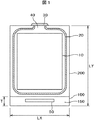
図1は本発明が適用される例としての、携帯電話等に使用される液晶表示装置の平面図である。
図1において、TFT基板100上に対向基板200が設置されている。TFT基板100と対向基板200の間に液晶層300が挟持されている。TFT基板100と対向基板200とは額縁部に形成されたシール材20によって接着している。TFT基板100は対向基板200よりも大きく形成されており、TFT基板100が対向基板200よりも大きくなっている部分には、液晶セル1に電源、映像信号、走査信号等を供給するための端子部150が形成されている。また、端子部150には、走査線、映像信号線等を駆動するためのICドライバ50が設置されている。
FIG. 1 is a plan view of a liquid crystal display device used in a mobile phone or the like as an example to which the present invention is applied.
In FIG. 1, a
図1において、液晶セル1の縦径LYは、例えば81mm、横径LXは、例えば54mmである。また、ICドライバ50等が搭載されている端子部150の幅はTは2.7mmである。表示領域10からTFT基板100または対向基板200の端部までが額縁部である。額縁部には、シール材20の他、図示しない走査線の引出し線等が設置される。
In FIG. 1, the vertical diameter LY of the
図1において、シール材20は熱硬化性のエポキシ樹脂で形成されている。シール材20は先ず対向基板200にスクリーン印刷によって塗布され、TFT基板100と重ねあわされる。その後、ベーキングによってシール材20を硬化させた後、液晶を注入し、注入孔40を封止材30によって封止する。
In FIG. 1, the
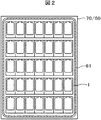
図1に示す液晶表示装置は小型なので、一個ずつ製造したのでは、効率が悪い。そこで、図2に示すように、大型の基板に複数の液晶セル1を形成し、その後、個々の液晶セル1に分離する。なお、本明細書では、ICドライバ50等が取り付けられて完成した表示装置を液晶表示装置と称し、TFT基板100と対向基板200が重ねあわされたものを液晶セル1と称する。
Since the liquid crystal display device shown in FIG. 1 is small, it is inefficient if manufactured one by one. Therefore, as shown in FIG. 2, a plurality of
図2において、マザーTFT基板60とマザー対向基板70が個々の液晶セル1のシール材20および、マザー基板シール材61を介して重ね合わされている。マザー基板シール材61は、マザー基板完成後、TFT基板100および対向基板200を研磨によって薄くする際に、研磨液が内部に入り込むことを防止するために形成される。したがって、TFT基板100あるいは、対向基板200を研磨する必要が無ければマザー基板シール材61は不用である。
In FIG. 2, the mother TFT substrate 60 and the mother counter substrate 70 are overlapped with each other through the sealing
図2において、各液晶セル1のシール材20、あるいは、マザー基板シール材61はスクリーン印刷によって、マザー対向基板70に形成される。スクリーン印刷によるシール材20の形成は従来行われていたディスペンサによるシール材20形成よりも効率よく行うことが出来る。しかし、後で説明するように、スクリーン印刷をする際のメッシュの接触によるムラを対策する必要がある。
In FIG. 2, the
本発明は液晶表示装置の駆動方法に限らず、種々の液晶表示装置に適用することが出来るが、本実施形態では、IPS(In Plane Switching)方式の液晶表示装置を例にとって説明する。図3は図1に示す表示領域10の断面図である。なお、IPSにも種々の方式があるが、図3はその1例である。図3はIPSのTFT付近の断面図である。図3において、ガラスで形成されるTFT基板100の上に、ゲート電極101が形成されている。ゲート電極101は走査線と同層で形成されている。ゲート電極101はAlNd合金の上にMoCr合金が積層されている。
The present invention is not limited to the driving method of the liquid crystal display device, and can be applied to various liquid crystal display devices. In the present embodiment, an IPS (In Plane Switching) type liquid crystal display device will be described as an example. FIG. 3 is a cross-sectional view of the
ゲート電極101を覆ってゲート絶縁膜102がSiNによって形成されている。ゲート絶縁膜102の上に、ゲート電極101と対向する位置に半導体層103がa−Si膜によって形成されている。a−Si膜はプラズマCVDによって形成される。a−Si膜はTFTのチャネル部を形成するが、チャネル部を挟んでa−Si膜上にソース電極104とドレイン電極105が形成される。なお、a−Si膜とソース電極104あるいはドレイン電極105との間には図示しないn+Si層が形成される。半導体層とソース電極104あるいはドレイン電極105とのオーミックコンタクトを取るためである。
A
ソース電極104は映像信号線が兼用し、ドレイン電極105は画素電極110と接続される。ソース電極104もドレイン電極105も同層で同時に形成される。本実施例では、ソース電極104あるいはドレイン電極105はMoCr合金で形成される。ソース電極104あるいはドレイン電極105の電気抵抗を下げたい場合は、例えば、AlNd合金をMoCr合金でサンドイッチした電極構造が用いられる。
The
TFTを覆って無機パッシベーション膜106がSiNによって形成される。無機パッシベーション膜106はTFTの、特にチャネル部を不純物から保護する。無機パッシベーション膜106の上には有機パッシベーション膜107が形成される。有機パッシベーション膜107はTFTの保護と同時に表面を平坦化する役割も有するので、厚く形成される。厚さは1μmから4μmである。
An
有機パッシベーション膜107には感光性のアクリル樹脂、シリコン樹脂、あるいはポリイミド樹脂等が使用される。有機パッシベーション膜107には、画素電極110とドレイン電極105が接続する部分にスルーホールを形成する必要があるが、有機パッシベーション膜107は感光性なので、フォトレジストを用いずに、有機パッシベーション膜107自体を露光、現像して、スルーホールを形成することが出来る。
A photosensitive acrylic resin, silicon resin, polyimide resin, or the like is used for the
有機パッシベーション膜107の上には対向電極108が形成される。対向電極108は透明導電膜であるITO(Indium Tin Oxide)を表示領域10全体にスパッタリングすることによって形成される。すなわち、対向電極108は面状に形成される。対向電極108を全面にスパッタリングによって形成した後、画素電極110とドレイン電極105を導通するためのスルーホール部だけは対向電極108をエッチングによって除去する。
A
対向電極108を覆って上部絶縁膜109がSiNによって形成される。上部電極が形成された後、エッチングによってスルーホールを形成する。この上部絶縁膜109をレジストにして無機パッシベーション膜106をエッチングしてスルーホール111を形成する。その後、上部絶縁膜109およびスルーホール111を覆って画素電極110となるITOをスパッタリングによって形成する。スパッタリングしたITOをパターニングして画素電極110を形成する。画素電極110となるITOはスルーホール111にも被着される。スルーホール111において、TFTから延在してきたドレイン電極105と画素電極110が導通し、映像信号が画素電極110に供給されることになる。
An upper insulating
画素電極110は、両端が閉じた櫛歯状の電極である。櫛歯状の電極と櫛歯状の電極の間はスリット112となっている。対向電極108には一定電圧が印加され、画素電極110には映像信号による電圧が印加される。画素電極110に電圧が印加されると図1に示すように、電気力線が発生して液晶分子301を電気力線の方向に回転させてバックライトからの光の透過を制御する。画素毎にバックライトからの透過が制御されるので、画像が形成されることになる。なお、画素電極110の上には液晶分子301を配向させるための配向膜113が形成されている。
The
図3の例では、有機パッシベーション膜107の上に、面状に形成された対向電極108が配置され、上部絶縁膜109の上に櫛歯電極110が配置されている。しかしこれとは逆に、有機パッシベーション膜107の上に面状に形成された画素電極110を配置し、上部絶縁膜109の上に櫛歯状の対向電極108が配置される場合もある。
In the example of FIG. 3, a
図3において、液晶層300を挟んで対向基板200が設置されている。対向基板200の内側には、カラーフィルタ201が形成されている。カラーフィルタ201は画素毎に、赤、緑、青のカラーフィルタ201が形成されており、カラー画像が形成される。カラーフィルタ201とカラーフィルタ201の間には遮光膜202が形成され、画像のコントラストを向上させている。なお、遮光膜202はTFTの遮光膜202としての役割も有し、TFTに光電流が流れることを防止している。
In FIG. 3, the
本発明では、遮光膜202の上にもカラーフィルタ201が2層形成されている。後で詳細に説明するように、シール材20をスクリーン印刷によって形成する際、スクリーン印刷のメッシュが画素領域の配向膜113に接触して、配向膜113にダメージを与え、画像にムラが発生することを防止するためである。
In the present invention, two
カラーフィルタ201および遮光膜202を覆ってオーバーコート膜203が形成されている。オーバーコート膜203は2つの役割を有している。すなわち、カラーフィルタ材料が液晶層300を汚染することを防止することと、カラーフィルタ201表面の過度の凹凸を緩和することである。オーバーコート膜203の上には、液晶の初期配向を決めるための配向膜113が形成されている。
An
IPSにおいては、配向膜表面のいわゆるティルト角が小さい。配向膜表面のいわゆるティルト角が小さいと、後で説明するスクリーン印刷時において、メッシュが対向基板の表示領域に接触することによる画像ムラに対する影響が大きくなる。したがって、この影響を軽減する本発明は、IPS方式の液晶表示装置において特に効果がある。 In IPS, the so-called tilt angle of the alignment film surface is small. If the so-called tilt angle on the surface of the alignment film is small, the influence on the image unevenness caused by the mesh contacting the display area of the counter substrate becomes large during screen printing described later. Therefore, the present invention for reducing this influence is particularly effective in an IPS liquid crystal display device.
なお、図3はIPS方式の液晶表示装置であるから、対向電極はTFT基板100側に形成されており、対向基板200側には形成されていない。このように、IPSでは、対向基板200の内側には導電膜が形成されていない。そうすると、対向基板200の電位が不安定になる。また、外部からの電磁ノイズが液晶層300に侵入し、画像に対して影響を与える。このような問題を除去するために、対向基板200の外側に表面導電膜210が形成される。表面導電膜210は、透明導電膜であるITOをスパッタリングすることによって形成される。
3 shows an IPS liquid crystal display device, the counter electrode is formed on the
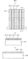
シール材20をスクリーン印刷によって形成する際、スクリーン印刷のためのメッシュが表示領域10に形成されているカラーフィルタ201上の配向膜113と接触すると、その接触部において、配向膜113が影響を受け、ムラが発生する。図9は従来例の対向基板200における画素構成を示し、図9(a)はその平面図である。
When the sealing
図9(a)において、遮光膜202が横方向にストライプ状に、TFT基板100の走査線と同じピッチによって形成されている。遮光膜202は、走査線上、あるいは走査線付近に形成されるTFTを外光から保護する役割を有する。遮光膜202の上を赤カラーフィルタ201R、青カラーフィルタ201B、緑カラーフィルタ201Gが特定間隔をもって、縦方向にストライプ状に形成されている。カラーフィルタ201の形成順序は例えば、赤カラーフィルタ201R、青カラーフィルタ201B、緑カラーフィルタ201Gの順である。
In FIG. 9A, the
図9(b)は図9(a)のA−A断面図である。図9(b)は遮光膜202上にカラーフィルタ201が重なって形成された部分の断面を表している。図9(c)は図9(a)のB−B断面図である。B−B断面図は緑カラーフィルタ201G上の断面を示している。図9(c)において、緑カラーフィルタ201Gは一部、遮光膜202を覆って形成されているので、この部分は他の部分よりも高くなっており、段差が形成されている。遮光膜202の膜厚は例えば、1.2μmであるから、段差はこの状態では、1.2μm程度形成されている。
FIG.9 (b) is AA sectional drawing of Fig.9 (a). FIG. 9B shows a cross section of a portion where the
図9はオーバーコート膜203が形成されていない状態である。図9に対してオーバーコート膜203が形成された場合の断面図が図10である。オーバーコート膜203が形成されると、遮光膜202上と他の部分との段差は緩和される。オーバーコート膜203の上にはさらに配向膜113が形成される。図10において、遮光膜202上の部分と他の部分の段差hは96nm程度となる。
FIG. 9 shows a state where the
配向膜113の膜厚は小さいので、段差に対する影響はオーバーコート膜203の影響が支配的である。つまり、この場合の段差hはオーバーコート膜203の厚さによっても変化する。すなわち、オーバーコート膜203の厚さが大きいほど段差は小さくなる。図10の場合の段差は、遮光膜202上におけるオーバーコート膜203の厚さを1.5μmとなる程度に遮光膜202を形成した場合の段差である。
Since the thickness of the
対向基板200にシール材20を形成するときの表示領域10の断面は図10のような状態となっている。シール材20をスクリーン印刷によって形成する場合は、スクリーン印刷のメッシュが有効面に接触する。遮光膜202上の配向膜113に接触しても画像には影響は無いが、遮光膜202が無い部分の配向膜113にメッシュが接触すると、画像ムラが生ずる。図10のような構成は、遮光膜202が形成された部分と他の部分では、96nm程度の段差が存在するが、この程度の段差では、メッシュは遮光膜202上と他の部分の両方に接触することになり、画像のムラは回避することが出来ない。ちなみに、この場合のスクリーン印刷におけるメッシュの影響によるムラの発生率は13.9%である。
The cross section of the
本発明は、対向基板200を以下の実施例のような構成とすることによって、スクリーン印刷機のメッシュによる画像のムラを防止するものである。
In the present invention, the
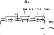
図4は本発明の第1の実施例を示す、対向基板200の表示領域10の構成である。
図4(a)は表示領域10の画素構造の平面図であり、図4(b)は図4(a)のA−A断面図であり、図4(c)は図4(a)のB−B断面図である。図4(a)において、赤カラーフィルタ201R、青カラーフィルタ201B、緑カラーフィルタ201Gが各々所定間隔をおいて縦方向に延在している。図4におけるカラーフィルタ201の形成順序は赤カラーフィルタ201R、青カラーフィルタ201B、緑カラーフィルタ201Gの順である。
FIG. 4 shows the configuration of the
4A is a plan view of the pixel structure of the
青カラーフィルタ201Bは、縦方向のみでなく、横方向に延在する遮光膜202を覆って横方向にも延在している。したがって、遮光膜202上では、青カラーフィルタ201Bと赤カラーフィルタ201R、あるいは青カラーフィルタ201Bと緑カラーフィルタ201Gが重なって形成されている。すなわち、赤カラーフィルタ201Rと緑カラーフィルタ201Gにおいて、遮光膜202上では、遮光膜202無い部分に比較して、遮光膜202の厚さと青カラーフィルタの厚さの分、高くなっている。
The
図4(b)は図4(a)のA−A断面図である。図4(b)は、横方向に延在する遮光膜202に沿った断面図となっている。図4(b)に示すように、赤カラーフィルタ201Rおよび緑カラーフィルタ201Gが形成された部分では、遮光膜202上には2層のカラーフィルタが形成されている。一方、青カラーフィルタ201Bの部分では、遮光膜202上には、青カラーフィルタ201B一層のみが形成されている。
FIG. 4B is a cross-sectional view taken along the line AA in FIG. FIG. 4B is a cross-sectional view along the
図4(c)は図4(a)のB―B断面図である。図4(c)は緑カラーフィルタ201Gに沿った断面図である。カラーフィルタ201の厚さは、例えば、3μm程度で、遮光膜202の厚さは例えば、1.3μmである。したがって、緑カラーフィルタ201Gにおいては、遮光膜202上と他の部分とでは、4.3μmの段差が形成されることになる。この状態は赤カラーフィルタ201Rにおいても同様である。
FIG. 4C is a cross-sectional view taken along the line BB in FIG. FIG. 4C is a cross-sectional view taken along the
実際の製品では、カラーフィルタ201の上にオーバーコート膜203が形成され、さらにその上に配向膜113が形成される。この状態を図5に示す。配向膜113の厚さは薄いので、図5における段差hに対しては、オーバーコート膜203の影響が支配的である。
In an actual product, an
図5において、オーバーコート膜203を例えば、遮光膜202上において1.5μm程度になるような厚さに形成した場合、図5における段差hは、409nm程度となる。図5は緑カラーフィルタ201Gにおける段差であるが、この状況は赤カラーフィルタ201R上においても同様である。一方、青カラーフィルタ201B上における段差は従来と同様である。
In FIG. 5, when the
このような状態における対向基板200に対して、スクリーン印刷によってシール材20を形成した場合、スクリーン印刷機のメッシュによる画像ムラの発生率は9.7%程度である。これは従来例である、13.9%に対して大幅に改善されるが、まだ十分とはいえない。
When the sealing
これに対し、図5における遮光膜202上のオーバーコート膜203の厚さを1μm程度に薄く形成すると、図5における段差hは大きくなって、750nm程度となる。このような状態における対向基板200に対して、スクリーン印刷によってシール材20を形成した場合、スクリーン印刷機のメッシュによる画像ムラの発生率は皆無となった。
On the other hand, when the thickness of the
すなわち、遮光膜202部分の高さが、他の部分の高さより、大幅に高いので、スクリーン印刷機のメッシュが遮光膜202部分によって支えられ、遮光膜202が無い部分、すなわち、画像を形成する部分のカラーフィルタ201とメッシュが接触してダメージを受けることを防止することが出来る。
That is, since the height of the
なお、本実施例では、赤カラーフィルタ201Rに沿った段差hと緑カラーフィルタ201Gに沿った段差hのみが大きく、青カラーフィルタ201Bに沿った段差hは従来と同様であるが、スクリーン印刷時のメッシュに対しては、赤カラーフィルタ201Rと緑カラーフィルタ201Gの高い部分がストッパーとなるので、青カラーフィルタ201Bに対するダメージも避けることが出来る。
In this embodiment, only the level difference h along the
同様にして、遮光膜202上にカラーフィルタ201を2層形成し、かつ、オーバーコート膜203の厚さを変化させることによって画像に対するスクリーン印刷機のメッシュの影響を調査をすると、図5における段差hが600nm以上となると、画像のムラに対するメッシュの影響を無くすることが出来る。
Similarly, when the influence of the screen printing machine mesh on the image is investigated by forming two layers of the
TFT基板100と対向基板200は液晶を挟持するために、特定間隔を持って配置されている。この特定間隔は、一般には、対向基板200に形成されるSOC205(Spacer On Color Filter)によって維持される。SOC205は感光性のアクリル樹脂等を露光、現像することによって形成される。
The
図6(a)は対向基板200にSOC205が形成された状態を示す平面図であり、図6(b)は、図6(a)のC−C断面図である。図6(a)および図6(b)に示すように、SOC205は、遮光膜202上で、青カラーフィルタ201Bの上で、オーバーコート膜203上に形成される。SOC205の高さは例えば、3.5μm程度である。
6A is a plan view showing a state where the
図5あるいは図6(b)に示す段差hは、当然、3.5μmを越えてはならない。また、段差hがSOC205の高さに近いと、液晶の配向乱れが顕著になる。実験によれば、段差hがSOC205の高さの半分程度である1.8μmまでであれば、顕著な配向乱れは観測されない。
Naturally, the step h shown in FIG. 5 or FIG. 6B should not exceed 3.5 μm. Further, when the step h is close to the height of the
このように、図5あるいは図6(b)における段差hを600nm以上、1.8μm以下とすることによって、シール材20をスクリーン印刷で形成するときのメッシュによるムラを抑制することが出来る。
In this way, by setting the step h in FIG. 5 or FIG. 6B to 600 nm or more and 1.8 μm or less, unevenness due to the mesh when the sealing
本実施例では、カラーフィルタ201の製造順番は赤カラーフィルタ201R、青カラーフィルタ201B、緑カラーフィルタ201Gの順としたが、カラーフィルタの製造順番はこれに限る必要は無い。また、本実施例では、遮光膜202と同じ方向に延在して遮光膜202を覆うカラーフィルタ201は青カラーフィルタ201Bとしたが、これに限らず、カラーフィルタ201の製造順番をかえることに合わせて他の色のカラーフィルタを遮光膜202を覆って遮光膜202と同じ方向に延在させても良い。
In this embodiment, the manufacturing order of the
図7は本発明の第2の実施例を示す対向基板200の画素構成である。図7(a)は本実施例の構成を示す平面図であり、図7(b)は図7(a)のA−A断面図、図7(c)は図7(a)のB−B断面図である。図7(a)において、赤カラーフィルタ201R、青カラーフィルタ201B、緑カラーフィルタ201Gが縦方向に延在している。また、各カラーフィルタは縦方向のみでなく、横方向にも特定ピッチで延在している。図7(a)においては、緑カラーフィルタ201Gのみが横方向にも延在しているように見えるが、緑カラーフィルタ201Gの下には、青カラーフィルタ201B、赤カラーフィルタ201Rも横方向に延在している。遮光膜202が特定ピッチで横方向に延在しているが、図7(a)においては緑カラーフィルタ201Gに覆われているので、図示されていない。
FIG. 7 shows a pixel configuration of the
図7(b)は図7(a)のA−A断面図であり、遮光膜202に沿った断面を示す図である。図7(b)に示すように、遮光膜202上では、赤カラーフィルタ201R、青カラーフィルタ201B、緑カラーフィルタ201Gの3層のカラーフィルタ201が形成されている。
FIG. 7B is a cross-sectional view taken along the line AA in FIG. 7A, and shows a cross section along the
図7(c)は図7(a)のB−B断面図であり、緑カラーフィルタ201Gに沿った断面構造を示している。図7(c)に示すように、遮光膜202上では3層のカラーフィルタ201が重なっている。遮光膜202の厚さは1.3μmであり、各カラーフィルタ201は3μm程度である。したがって遮光膜202上と他の部分のあいだには、7.3μmというような大きな段差が存在する。
FIG. 7C is a BB cross-sectional view of FIG. 7A and shows a cross-sectional structure along the
実際の製品では、図8に示すように、緑カラーフィルタ201Gの上にオーバーコート膜203および配向膜113が形成される。オーバーコート膜203が形成される前は、7.3μmというように大きな段差が形成されるが、オーバーコート膜203および配向膜113が形成された後の段差hは小さくなる。
In an actual product, as shown in FIG. 8, an
しかし、オーバーコート膜203形成前の段差がもともと大きいので、オーバーコート膜203を遮光膜202上で1.5μm程度としても、図8に示す段差hは容易に600nm以上とすることが出来る。一方、配向乱れの制約から、図8における段差hは1.8μm以下とする必要があることは実施例1と同様である。
However, since the step before the
以上のように、本実施例によれば、遮光膜202上とその他の部分の段差hを容易に600nm以上とすることが出来るので、スクリーン印刷によってシール材20を形成する際のメッシュの影響によるムラを防止することが出来る。
As described above, according to the present embodiment, the step h between the
すなわち、遮光膜の上に3層のカラーフィルタを重ねることによって形成された凸部がスクリーン印刷時のメッシュのストッパーとなり、遮光膜が形成されていない部分、つまり画素領域の配向膜にメッシュが接触することを防止することが出来る。 That is, the convex part formed by overlaying three layers of color filters on the light shielding film serves as a mesh stopper during screen printing, and the mesh contacts the part where the light shielding film is not formed, that is, the alignment film in the pixel region. Can be prevented.
本実施例では、カラーフィルタ201の製造順番は赤カラーフィルタ201R、青カラーフィルタ201B、緑カラーフィルタ201Gとしたが、順番はこれに限る必要は無い。各カラーフィルタの形成の順番が異なっても、遮光膜上に3層のカラーフィルタが形成されることには変わりが無いからである。
In this embodiment, the manufacturing order of the
尚、遮光膜は、樹脂に限らずクロムのような金属で形成することも可能である。また、本明細書では遮光膜を横方向のストライブ状に形成しているが、縦方向の各カラーフィルタの境界をも覆うようにマトリクス状に形成することも可能である。また、本明細書では、カラーフィルタ上にオーバーコート膜を設けているが、カラーフィルタの顔料による液晶層への汚染が問題とならない等の場合は、オーバーコート膜を設けない構造とすることも可能である。この場合は、本発明の構成により、画素領域の配向膜にメッシュが接触することを防止する効果が大きい。 The light shielding film is not limited to resin, and can be formed of a metal such as chromium. In this specification, the light shielding film is formed in a stripe shape in the horizontal direction, but may be formed in a matrix shape so as to cover the boundaries of the color filters in the vertical direction. In this specification, an overcoat film is provided on the color filter. However, when the contamination of the liquid crystal layer by the color filter pigment is not a problem, the overcoat film may not be provided. Is possible. In this case, the configuration of the present invention has a great effect of preventing the mesh from contacting the alignment film in the pixel region.
また、表示性能の向上を図るためにRGBのカラーフィルタの膜厚を異ならせることも可能である。例えば、赤、緑のカラーフィルタに対し、青のカラーフィルタの膜厚を小さくすることも可能である。この場合、図4及び図6の実施形態においてメッシュ状とするカラーフィルタを赤、或いは、緑とすることで、カラーフィルタを積層して得られる凸部の高さを高くすることが可能となる。 It is also possible to change the film thickness of the RGB color filters in order to improve display performance. For example, it is possible to reduce the film thickness of the blue color filter relative to the red and green color filters. In this case, it is possible to increase the height of the convex portion obtained by stacking the color filters by setting the color filter having a mesh shape in the embodiment of FIGS. 4 and 6 to red or green. .
また、図6では、SOCを青のカラーフィルタ上に形成しているが、カラーフィルタが2層、或いは、3層積層された箇所にSOCを形成するものであってもよい。 In FIG. 6, the SOC is formed on the blue color filter. However, the SOC may be formed at a location where two or three color filters are laminated.
以上の実施例はIPS方式の液晶表示装置について説明したが、本発明はIPS方式の液晶表示装置に限らず、TN方式、VA方式等、他の液晶表示装置についても適用することが出来る。 In the above embodiments, the IPS liquid crystal display device has been described. However, the present invention is not limited to the IPS liquid crystal display device, but can be applied to other liquid crystal display devices such as the TN method and the VA method.
1…液晶セル、 10…表示領域、 20…シール材、 30…封止材、 40…注入孔、 50…ICドライバ、 60…マザーTFT基板、 61…マザー基板シール材、 70…マザー対向基板、 100…TFT基板、 101…ゲート電極、 103…半導体層、 104…ソース電極、 105…ドレイン電極、 106…無機パッシベーション膜、 107…有機パッシベーション膜、 108…対向電極、 109…上部絶縁膜、 110…画素電極、 111…スルーホール、 112…スリット、 113…配向膜、 200…対向基板、 201…カラーフィルタ、 201R…赤カラーフィルタ、 201B…青カラーフィルタ、 201G…緑カラーフィルタ、 202…遮光膜、 203…オーバーコート膜、 205…SOC、 210…表面導電膜、 300…液晶層、 301…液晶分子。
DESCRIPTION OF
Claims (6)
前記対向基板には遮光膜が第1の方向に延在して第2の方向に配列し、赤カラーフィルタが第2の方向に延在して第1の方向に配列し、青カラーフィルタが第2の方向に延在して第1の方向に配列し、緑カラーフィルタが第2の方向に延在して第1の方向に配列し、
前記赤カラーフィルタ、前記青カラーフィルタ、前記緑カラーフィルタのうちの一色のカラーフィルタは、前記遮光膜を覆って第1の方向に延在し、前記一色のカラーフィルタが、前記第1の方向に延在した部分では、2層のカラーフィルタが形成されており、
前記赤カラーフィルタ、前記青カラーフィルタ、および、前記緑カラーフィルタを覆ってオーバーコート膜が形成され、前記オーバーコート膜を覆って配向膜が形成されていることを特徴とする液晶表示装置。 A TFT substrate in which pixels including a pixel electrode and a TFT are formed in a matrix, a counter substrate on which a color filter is formed, a liquid crystal is sandwiched between the TFT substrate and the color filter, and the TFT substrate is opposed to the TFT substrate. The substrate is a liquid crystal display device bonded through a sealing material formed around the counter substrate,
On the counter substrate, a light shielding film extends in the first direction and is arranged in the second direction, a red color filter extends in the second direction and is arranged in the first direction, and a blue color filter is arranged Extending in the second direction and arranged in the first direction, the green color filter extending in the second direction and arranged in the first direction;
One color filter of the red color filter, the blue color filter, and the green color filter extends in a first direction so as to cover the light shielding film, and the one color filter is in the first direction. In the part extending to 2 layers of color filters are formed,
A liquid crystal display device, wherein an overcoat film is formed to cover the red color filter, the blue color filter, and the green color filter, and an alignment film is formed to cover the overcoat film.
前記対向基板には遮光膜が第1の方向に延在して第2の方向に配列し、赤カラーフィルタが第2の方向に延在して第1の方向に配列するとともに、前記遮光膜を覆って前記第1の方向に延在して第2の方向に配列し、青カラーフィルタが第2の方向に延在して第1の方向に配列するとともに、前記遮光膜を覆って前記第1の方向に延在して第2の方向に配列し、緑カラーフィルタが第2の方向に延在して第1の方向に配列するとともに、前記遮光膜を覆って前記第1の方向に延在して第2の方向に配列し、
前記赤カラーフィルタ、前記青カラーフィルタ、および、前記緑カラーフィルタを覆ってオーバーコート膜が形成され、前記オーバーコート膜を覆って配向膜が形成されていることを特徴とする液晶表示装置。 A TFT substrate in which pixels including pixels and TFTs are formed in a matrix, a counter substrate on which a color filter is formed, a liquid crystal is sandwiched between the TFT substrate and the color filter, and the TFT substrate is opposed to the TFT substrate. The substrate is a liquid crystal display device bonded through a sealing material formed around the counter substrate,
On the counter substrate, a light shielding film extends in the first direction and is arranged in the second direction, a red color filter extends in the second direction and is arranged in the first direction, and the light shielding film Extending in the first direction and arranged in the second direction, the blue color filter extending in the second direction and arranged in the first direction, and covering the light shielding film and Extending in the first direction and arranged in the second direction, the green color filter extending in the second direction and arranged in the first direction, and covering the light shielding film, the first direction Extending in the second direction,
A liquid crystal display device, wherein an overcoat film is formed to cover the red color filter, the blue color filter, and the green color filter, and an alignment film is formed to cover the overcoat film.
Priority Applications (2)
| Application Number | Priority Date | Filing Date | Title |
|---|---|---|---|
| JP2008189604A JP5156517B2 (en) | 2008-07-23 | 2008-07-23 | Liquid crystal display |
| US12/506,437 US8749734B2 (en) | 2008-07-23 | 2009-07-21 | Liquid crystal display device with layers of different color filters covering light shielding films |
Applications Claiming Priority (1)
| Application Number | Priority Date | Filing Date | Title |
|---|---|---|---|
| JP2008189604A JP5156517B2 (en) | 2008-07-23 | 2008-07-23 | Liquid crystal display |
Publications (2)
| Publication Number | Publication Date |
|---|---|
| JP2010026368A true JP2010026368A (en) | 2010-02-04 |
| JP5156517B2 JP5156517B2 (en) | 2013-03-06 |
Family
ID=41568332
Family Applications (1)
| Application Number | Title | Priority Date | Filing Date |
|---|---|---|---|
| JP2008189604A Active JP5156517B2 (en) | 2008-07-23 | 2008-07-23 | Liquid crystal display |
Country Status (2)
| Country | Link |
|---|---|
| US (1) | US8749734B2 (en) |
| JP (1) | JP5156517B2 (en) |
Cited By (2)
| Publication number | Priority date | Publication date | Assignee | Title |
|---|---|---|---|---|
| KR101791546B1 (en) * | 2011-07-05 | 2017-10-31 | 삼성디스플레이 주식회사 | Display substrate and method of repairing the same |
| JP2019003004A (en) * | 2017-06-14 | 2019-01-10 | 三菱電機株式会社 | Liquid crystal display device |
Families Citing this family (10)
| Publication number | Priority date | Publication date | Assignee | Title |
|---|---|---|---|---|
| JP2011053608A (en) * | 2009-09-04 | 2011-03-17 | Mitsubishi Electric Corp | Method of manufacturing liquid crystal panel |
| JP6605789B2 (en) * | 2013-06-18 | 2019-11-13 | パナソニック インテレクチュアル プロパティ コーポレーション オブ アメリカ | Transmission method, reception method, transmission device, and reception device |
| CN104166273A (en) * | 2014-06-26 | 2014-11-26 | 京东方科技集团股份有限公司 | Display substrate, display substrate mother board and display device |
| CN104950527A (en) * | 2015-07-01 | 2015-09-30 | 合肥鑫晟光电科技有限公司 | Display substrate, manufacturing method thereof, display panel and display device |
| KR102408899B1 (en) * | 2015-10-02 | 2022-06-15 | 엘지디스플레이 주식회사 | Liquid crystal display device and method for manufacturing the same |
| KR20170130660A (en) * | 2016-05-18 | 2017-11-29 | 삼성디스플레이 주식회사 | Display device |
| JP2018124480A (en) | 2017-02-02 | 2018-08-09 | 株式会社ジャパンディスプレイ | Display device |
| CN108983479B (en) | 2017-06-01 | 2019-11-05 | 京东方科技集团股份有限公司 | Display base plate and preparation method thereof and display device |
| CN109116615A (en) * | 2018-08-20 | 2019-01-01 | 深圳市华星光电技术有限公司 | Color membrane substrates and liquid crystal display panel |
| CN111413823A (en) | 2019-01-07 | 2020-07-14 | 群创光电股份有限公司 | Electronic device |
Citations (4)
| Publication number | Priority date | Publication date | Assignee | Title |
|---|---|---|---|---|
| JPH0664359A (en) * | 1992-08-24 | 1994-03-08 | Matsushita Electric Ind Co Ltd | Screen printing plate |
| JPH1010520A (en) * | 1996-06-19 | 1998-01-16 | Dainippon Printing Co Ltd | Color filter for ferroelectric liquid crystal, and ferooelectric liquid crystal display device using the same |
| JP2002023148A (en) * | 2000-04-18 | 2002-01-23 | Semiconductor Energy Lab Co Ltd | Electrooptical device |
| JP2007052360A (en) * | 2005-08-19 | 2007-03-01 | Toshiba Matsushita Display Technology Co Ltd | Color filter substrate, liquid crystal display panel, and method for manufacturing a plurality of color filter substrates |
Family Cites Families (4)
| Publication number | Priority date | Publication date | Assignee | Title |
|---|---|---|---|---|
| US4758734A (en) * | 1984-03-13 | 1988-07-19 | Nec Corporation | High resolution image sensor array using amorphous photo-diodes |
| JPH0721562B2 (en) * | 1987-05-14 | 1995-03-08 | 凸版印刷株式会社 | Color filter |
| DE68920702T2 (en) * | 1988-11-10 | 1995-06-14 | Toshiba Kawasaki Kk | Liquid crystal display device, color filter therefor, and method of manufacturing the color filter. |
| JP2003131020A (en) | 2001-10-26 | 2003-05-08 | Toppan Printing Co Ltd | Manufacturing method of color filter |
-
2008
- 2008-07-23 JP JP2008189604A patent/JP5156517B2/en active Active
-
2009
- 2009-07-21 US US12/506,437 patent/US8749734B2/en active Active
Patent Citations (4)
| Publication number | Priority date | Publication date | Assignee | Title |
|---|---|---|---|---|
| JPH0664359A (en) * | 1992-08-24 | 1994-03-08 | Matsushita Electric Ind Co Ltd | Screen printing plate |
| JPH1010520A (en) * | 1996-06-19 | 1998-01-16 | Dainippon Printing Co Ltd | Color filter for ferroelectric liquid crystal, and ferooelectric liquid crystal display device using the same |
| JP2002023148A (en) * | 2000-04-18 | 2002-01-23 | Semiconductor Energy Lab Co Ltd | Electrooptical device |
| JP2007052360A (en) * | 2005-08-19 | 2007-03-01 | Toshiba Matsushita Display Technology Co Ltd | Color filter substrate, liquid crystal display panel, and method for manufacturing a plurality of color filter substrates |
Cited By (3)
| Publication number | Priority date | Publication date | Assignee | Title |
|---|---|---|---|---|
| KR101791546B1 (en) * | 2011-07-05 | 2017-10-31 | 삼성디스플레이 주식회사 | Display substrate and method of repairing the same |
| JP2019003004A (en) * | 2017-06-14 | 2019-01-10 | 三菱電機株式会社 | Liquid crystal display device |
| JP7007817B2 (en) | 2017-06-14 | 2022-01-25 | トライベイル テクノロジーズ, エルエルシー | Liquid crystal display device |
Also Published As
| Publication number | Publication date |
|---|---|
| US8749734B2 (en) | 2014-06-10 |
| US20100020275A1 (en) | 2010-01-28 |
| JP5156517B2 (en) | 2013-03-06 |
Similar Documents
| Publication | Publication Date | Title |
|---|---|---|
| JP5156517B2 (en) | Liquid crystal display | |
| US8368864B2 (en) | Liquid crystal display device with spacer in the sealant | |
| US10473984B2 (en) | Liquid crystal display device | |
| US9417485B2 (en) | Liquid crystal display device | |
| JP5553531B2 (en) | Liquid crystal display | |
| US9977280B2 (en) | COT type liquid crystal display device | |
| US8421973B2 (en) | Liquid crystal display device | |
| JP5239924B2 (en) | Liquid crystal display device and electronic apparatus using the same | |
| JP6649788B2 (en) | Liquid crystal display | |
| KR20080026404A (en) | Array substrat, display panel having the same and fabricating of display panel | |
| US20210088855A1 (en) | Liquid crystal display device | |
| US20110216282A1 (en) | Liquid crystal display device | |
| KR20090130938A (en) | Display substrate and display apparatus having the same | |
| JP2018025670A (en) | Liquid crystal display device | |
| JP2004272012A (en) | Display apparatus | |
| JP2017187530A (en) | Liquid crystal display device | |
| JP4722538B2 (en) | Display device | |
| JP5275650B2 (en) | Liquid crystal display | |
| JP2009169162A (en) | Liquid crystal display | |
| KR20130018056A (en) | Liquid crystal display device | |
| US20100045914A1 (en) | Liquid crystal display device | |
| JP5492326B2 (en) | Manufacturing method of liquid crystal display device | |
| JP5026883B2 (en) | Electro-optical device and electronic apparatus | |
| JP2020013148A (en) | Liquid crystal display device | |
| JP2009271366A (en) | Liquid crystal display device |
Legal Events
| Date | Code | Title | Description |
|---|---|---|---|
| A711 | Notification of change in applicant |
Free format text: JAPANESE INTERMEDIATE CODE: A712 Effective date: 20110218 |
|
| RD03 | Notification of appointment of power of attorney |
Free format text: JAPANESE INTERMEDIATE CODE: A7423 Effective date: 20110218 |
|
| A621 | Written request for application examination |
Free format text: JAPANESE INTERMEDIATE CODE: A621 Effective date: 20110512 |
|
| A131 | Notification of reasons for refusal |
Free format text: JAPANESE INTERMEDIATE CODE: A131 Effective date: 20120828 |
|
| A977 | Report on retrieval |
Free format text: JAPANESE INTERMEDIATE CODE: A971007 Effective date: 20120829 |
|
| A521 | Request for written amendment filed |
Free format text: JAPANESE INTERMEDIATE CODE: A523 Effective date: 20121017 |
|
| TRDD | Decision of grant or rejection written | ||
| A01 | Written decision to grant a patent or to grant a registration (utility model) |
Free format text: JAPANESE INTERMEDIATE CODE: A01 Effective date: 20121113 |
|
| A61 | First payment of annual fees (during grant procedure) |
Free format text: JAPANESE INTERMEDIATE CODE: A61 Effective date: 20121210 |
|
| FPAY | Renewal fee payment (event date is renewal date of database) |
Free format text: PAYMENT UNTIL: 20151214 Year of fee payment: 3 |
|
| R150 | Certificate of patent or registration of utility model |
Ref document number: 5156517 Country of ref document: JP Free format text: JAPANESE INTERMEDIATE CODE: R150 Free format text: JAPANESE INTERMEDIATE CODE: R150 |
|
| R250 | Receipt of annual fees |
Free format text: JAPANESE INTERMEDIATE CODE: R250 |
|
| R250 | Receipt of annual fees |
Free format text: JAPANESE INTERMEDIATE CODE: R250 |
|
| R250 | Receipt of annual fees |
Free format text: JAPANESE INTERMEDIATE CODE: R250 |
|
| R250 | Receipt of annual fees |
Free format text: JAPANESE INTERMEDIATE CODE: R250 |
|
| R250 | Receipt of annual fees |
Free format text: JAPANESE INTERMEDIATE CODE: R250 |
|
| R250 | Receipt of annual fees |
Free format text: JAPANESE INTERMEDIATE CODE: R250 |
|
| S531 | Written request for registration of change of domicile |
Free format text: JAPANESE INTERMEDIATE CODE: R313531 |
|
| S533 | Written request for registration of change of name |
Free format text: JAPANESE INTERMEDIATE CODE: R313533 |
|
| R350 | Written notification of registration of transfer |
Free format text: JAPANESE INTERMEDIATE CODE: R350 |
|
| R250 | Receipt of annual fees |
Free format text: JAPANESE INTERMEDIATE CODE: R250 |
|
| R250 | Receipt of annual fees |
Free format text: JAPANESE INTERMEDIATE CODE: R250 |
|
| S111 | Request for change of ownership or part of ownership |
Free format text: JAPANESE INTERMEDIATE CODE: R313117 |
|
| R350 | Written notification of registration of transfer |
Free format text: JAPANESE INTERMEDIATE CODE: R350 |
|
| R250 | Receipt of annual fees |
Free format text: JAPANESE INTERMEDIATE CODE: R250 |