JP2010021384A - インダクタおよびフィルタ - Google Patents
インダクタおよびフィルタ Download PDFInfo
- Publication number
- JP2010021384A JP2010021384A JP2008180970A JP2008180970A JP2010021384A JP 2010021384 A JP2010021384 A JP 2010021384A JP 2008180970 A JP2008180970 A JP 2008180970A JP 2008180970 A JP2008180970 A JP 2008180970A JP 2010021384 A JP2010021384 A JP 2010021384A
- Authority
- JP
- Japan
- Prior art keywords
- inductor
- air bridge
- electrode
- substrate
- air
- Prior art date
- Legal status (The legal status is an assumption and is not a legal conclusion. Google has not performed a legal analysis and makes no representation as to the accuracy of the status listed.)
- Granted
Links
- 239000000758 substrate Substances 0.000 claims abstract description 38
- 229910001218 Gallium arsenide Inorganic materials 0.000 claims description 5
- 239000004065 semiconductor Substances 0.000 claims description 2
- 239000004020 conductor Substances 0.000 abstract description 14
- 239000010410 layer Substances 0.000 description 22
- 238000000034 method Methods 0.000 description 11
- 230000000052 comparative effect Effects 0.000 description 10
- 230000002500 effect on skin Effects 0.000 description 8
- 238000007747 plating Methods 0.000 description 8
- 238000004088 simulation Methods 0.000 description 8
- 238000010586 diagram Methods 0.000 description 7
- 238000003780 insertion Methods 0.000 description 7
- 230000037431 insertion Effects 0.000 description 7
- 239000003990 capacitor Substances 0.000 description 5
- 230000005855 radiation Effects 0.000 description 5
- 239000011347 resin Substances 0.000 description 5
- 229920005989 resin Polymers 0.000 description 5
- 239000012141 concentrate Substances 0.000 description 3
- PCHJSUWPFVWCPO-UHFFFAOYSA-N gold Chemical compound [Au] PCHJSUWPFVWCPO-UHFFFAOYSA-N 0.000 description 3
- 239000010931 gold Substances 0.000 description 3
- 229910052737 gold Inorganic materials 0.000 description 3
- 230000003071 parasitic effect Effects 0.000 description 3
- 239000004642 Polyimide Substances 0.000 description 2
- UMIVXZPTRXBADB-UHFFFAOYSA-N benzocyclobutene Chemical compound C1=CC=C2CCC2=C1 UMIVXZPTRXBADB-UHFFFAOYSA-N 0.000 description 2
- 230000008878 coupling Effects 0.000 description 2
- 238000010168 coupling process Methods 0.000 description 2
- 238000005859 coupling reaction Methods 0.000 description 2
- 230000000694 effects Effects 0.000 description 2
- 230000005672 electromagnetic field Effects 0.000 description 2
- 229920001721 polyimide Polymers 0.000 description 2
- 239000010409 thin film Substances 0.000 description 2
- 238000004804 winding Methods 0.000 description 2
- 229910018072 Al 2 O 3 Inorganic materials 0.000 description 1
- 229910004298 SiO 2 Inorganic materials 0.000 description 1
- RTAQQCXQSZGOHL-UHFFFAOYSA-N Titanium Chemical compound [Ti] RTAQQCXQSZGOHL-UHFFFAOYSA-N 0.000 description 1
- PNEYBMLMFCGWSK-UHFFFAOYSA-N aluminium oxide Inorganic materials [O-2].[O-2].[O-2].[Al+3].[Al+3] PNEYBMLMFCGWSK-UHFFFAOYSA-N 0.000 description 1
- FFBHFFJDDLITSX-UHFFFAOYSA-N benzyl N-[2-hydroxy-4-(3-oxomorpholin-4-yl)phenyl]carbamate Chemical compound OC1=C(NC(=O)OCC2=CC=CC=C2)C=CC(=C1)N1CCOCC1=O FFBHFFJDDLITSX-UHFFFAOYSA-N 0.000 description 1
- 230000005540 biological transmission Effects 0.000 description 1
- 230000015572 biosynthetic process Effects 0.000 description 1
- 238000004891 communication Methods 0.000 description 1
- 230000007547 defect Effects 0.000 description 1
- 230000000994 depressogenic effect Effects 0.000 description 1
- 239000011521 glass Substances 0.000 description 1
- 239000000463 material Substances 0.000 description 1
- 238000000206 photolithography Methods 0.000 description 1
- 229910052594 sapphire Inorganic materials 0.000 description 1
- 239000010980 sapphire Substances 0.000 description 1
- 239000002356 single layer Substances 0.000 description 1
- 239000007787 solid Substances 0.000 description 1
- 229910052719 titanium Inorganic materials 0.000 description 1
- 239000010936 titanium Substances 0.000 description 1
Images


Classifications
-
- H—ELECTRICITY
- H01—ELECTRIC ELEMENTS
- H01F—MAGNETS; INDUCTANCES; TRANSFORMERS; SELECTION OF MATERIALS FOR THEIR MAGNETIC PROPERTIES
- H01F17/00—Fixed inductances of the signal type
- H01F17/0006—Printed inductances
- H01F17/0013—Printed inductances with stacked layers
-
- H—ELECTRICITY
- H01—ELECTRIC ELEMENTS
- H01L—SEMICONDUCTOR DEVICES NOT COVERED BY CLASS H10
- H01L23/00—Details of semiconductor or other solid state devices
- H01L23/52—Arrangements for conducting electric current within the device in operation from one component to another, i.e. interconnections, e.g. wires, lead frames
- H01L23/522—Arrangements for conducting electric current within the device in operation from one component to another, i.e. interconnections, e.g. wires, lead frames including external interconnections consisting of a multilayer structure of conductive and insulating layers inseparably formed on the semiconductor body
- H01L23/5227—Inductive arrangements or effects of, or between, wiring layers
-
- H—ELECTRICITY
- H01—ELECTRIC ELEMENTS
- H01P—WAVEGUIDES; RESONATORS, LINES, OR OTHER DEVICES OF THE WAVEGUIDE TYPE
- H01P1/00—Auxiliary devices
- H01P1/20—Frequency-selective devices, e.g. filters
- H01P1/215—Frequency-selective devices, e.g. filters using ferromagnetic material
-
- H—ELECTRICITY
- H01—ELECTRIC ELEMENTS
- H01F—MAGNETS; INDUCTANCES; TRANSFORMERS; SELECTION OF MATERIALS FOR THEIR MAGNETIC PROPERTIES
- H01F17/00—Fixed inductances of the signal type
- H01F17/0006—Printed inductances
- H01F2017/0046—Printed inductances with a conductive path having a bridge
-
- H—ELECTRICITY
- H01—ELECTRIC ELEMENTS
- H01F—MAGNETS; INDUCTANCES; TRANSFORMERS; SELECTION OF MATERIALS FOR THEIR MAGNETIC PROPERTIES
- H01F17/00—Fixed inductances of the signal type
- H01F17/0006—Printed inductances
- H01F2017/0073—Printed inductances with a special conductive pattern, e.g. flat spiral
-
- H—ELECTRICITY
- H01—ELECTRIC ELEMENTS
- H01F—MAGNETS; INDUCTANCES; TRANSFORMERS; SELECTION OF MATERIALS FOR THEIR MAGNETIC PROPERTIES
- H01F27/00—Details of transformers or inductances, in general
- H01F27/40—Structural association with built-in electric component, e.g. fuse
-
- H—ELECTRICITY
- H01—ELECTRIC ELEMENTS
- H01L—SEMICONDUCTOR DEVICES NOT COVERED BY CLASS H10
- H01L2924/00—Indexing scheme for arrangements or methods for connecting or disconnecting semiconductor or solid-state bodies as covered by H01L24/00
- H01L2924/0001—Technical content checked by a classifier
- H01L2924/0002—Not covered by any one of groups H01L24/00, H01L24/00 and H01L2224/00
-
- H—ELECTRICITY
- H03—ELECTRONIC CIRCUITRY
- H03H—IMPEDANCE NETWORKS, e.g. RESONANT CIRCUITS; RESONATORS
- H03H1/00—Constructional details of impedance networks whose electrical mode of operation is not specified or applicable to more than one type of network
- H03H2001/0092—Inductor filters, i.e. inductors whose parasitic capacitance is of relevance to consider it as filter
Abstract
【解決手段】インダクタ10は、エアブリッジ部12とエアブリッジ部13とを備える。エアブリッジ部12は、基板1上の複数の支持位置11の間に、基板1から浮き上がる状態で架設される。エアブリッジ部13は、エアブリッジ部12上の複数の支持位置11の間に、第1のエアブリッジ部12から浮き上がる状態で架設される。これによりエアブリッジ部12とエアブリッジ部13とが並列に接続されて電流が分散し、エアブリッジ部12およびエアブリッジ部13それぞれでの導体損が低減する。
【選択図】図2
Description
Q=ωL/r
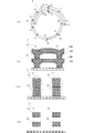
図1は第1の実施形態に係るインダクタの構成を示す図であり、(A)は上面図、(B)はB−B断面図、(C)は基板表面の平面図である。
このインダクタ10は、2GHz帯で利用するものであり、基板1と樹脂層8とインダクタ部7と端子電極6A,6Bとを備える。ここでは基板1として、比誘電率εr=12.9、誘電正接tanδ=2.4×10⁻⁴、基板厚み100μmのGaAs半導体基板を使用している。インダクタ部7は、上面形状が内径約300μm、巻き数1.5、電極幅約30μmのスパイラル状に構成した導体パターンからなる。樹脂層8は、ポリイミド(PI)やベンゾシクロブテン(BCB)などの絶縁性樹脂材料であり、基板1の表面のインダクタ部7の形成領域を含む範囲に厚み約25μmで形成している。端子電極6A,6Bは、インダクタ部7の両端に接続して形成している。
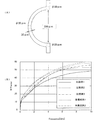
比較例1:1層のベタ電極(電極厚:6μm)
比較例2:1層のエアブリッジ電極(電極厚:6μm)
比較例3:1層のエアブリッジ電極(電極厚:12μm)
本構成例1:2層のエアブリッジ電極(電極厚:6μm)
本構成例2:3層のエアブリッジ電極(電極厚:6μm)
シミュレーションの結果、2GHzでのQ値は以下の通りであった。
比較例2:Q=28
比較例3:Q=30
本構成例1:Q=35
本構成例2:Q=34
本構成例1および2では、インダクタのQ値を比較例に比べて25%以上改善できた。また、本構成例2は、エアブリッジ電極の断面積が同一である比較例3に対しても、インダクタのQ値を約17%改善できた。以上のシミュレーション結果からも、本発明の効果によって、インダクタのQ値を改善できることが確認できた。
プロセス1:まず基板1上にレジストを形成し、露光およびレジスト除去により支持位置11に開口を設ける。
プロセス2:次にレジスト上および開口内にエアブリッジ部12となるメッキ電極を形成する。
プロセス3:次にその上にさらにレジストを形成し、露光およびレジスト除去により支持位置21に開口を設ける。
6A,6B…端子電極
7…インダクタ部
8…樹脂層
10,20…インダクタ
11.21…支持位置
12,13,23…エアブリッジ部
12A,13A…シード層
12B,13B…メッキ層
Claims (6)
- 基板上の複数の支持位置の間に、前記基板から浮き上がる状態で架設される第1のエアブリッジ電極と、
前記第1のエアブリッジ電極上の複数の支持位置の間に、前記第1のエアブリッジ電極から浮き上がる状態で架設される第2のエアブリッジ電極と、
を備えるインダクタ。 - 前記第1および第2のエアブリッジ電極は、インダクタ使用周波数における表皮深さよりも電極厚が大きい、請求項1に記載のインダクタ。
- 前記第2のエアブリッジ電極の支持位置は、前記第1のエアブリッジの支持位置に一致する、請求項1または2に記載のインダクタ。
- 前記第2のエアブリッジ電極の支持位置は、前記第1のエアブリッジの支持位置からずれる、請求項1または2に記載のインダクタ。
- 前記基板は、GaAs半導体基板である請求項1〜4のいずれかに記載のインダクタ。
- 請求項1〜5のいずれかに記載のインダクタを備えたフィルタ。
Priority Applications (5)
| Application Number | Priority Date | Filing Date | Title |
|---|---|---|---|
| JP2008180970A JP4656196B2 (ja) | 2008-07-11 | 2008-07-11 | インダクタおよびフィルタ |
| TW098109699A TWI409831B (zh) | 2008-07-11 | 2009-03-25 | 電感器及濾波器 |
| DE102009021088A DE102009021088A1 (de) | 2008-07-11 | 2009-05-13 | Induktor und Filter |
| US12/467,420 US8134221B2 (en) | 2008-07-11 | 2009-05-18 | Inductor and filter |
| CN2009101410642A CN101625920B (zh) | 2008-07-11 | 2009-05-18 | 电感器和滤波器 |
Applications Claiming Priority (1)
| Application Number | Priority Date | Filing Date | Title |
|---|---|---|---|
| JP2008180970A JP4656196B2 (ja) | 2008-07-11 | 2008-07-11 | インダクタおよびフィルタ |
Publications (2)
| Publication Number | Publication Date |
|---|---|
| JP2010021384A true JP2010021384A (ja) | 2010-01-28 |
| JP4656196B2 JP4656196B2 (ja) | 2011-03-23 |
Family
ID=41412956
Family Applications (1)
| Application Number | Title | Priority Date | Filing Date |
|---|---|---|---|
| JP2008180970A Expired - Fee Related JP4656196B2 (ja) | 2008-07-11 | 2008-07-11 | インダクタおよびフィルタ |
Country Status (5)
| Country | Link |
|---|---|
| US (1) | US8134221B2 (ja) |
| JP (1) | JP4656196B2 (ja) |
| CN (1) | CN101625920B (ja) |
| DE (1) | DE102009021088A1 (ja) |
| TW (1) | TWI409831B (ja) |
Families Citing this family (2)
| Publication number | Priority date | Publication date | Assignee | Title |
|---|---|---|---|---|
| JP6760247B2 (ja) | 2017-12-05 | 2020-09-23 | 株式会社村田製作所 | コイル部品 |
| CN111146185A (zh) * | 2019-05-30 | 2020-05-12 | 福建省福联集成电路有限公司 | 一种电感及其制作方法 |
Citations (8)
| Publication number | Priority date | Publication date | Assignee | Title |
|---|---|---|---|---|
| JPS4834686A (ja) * | 1971-09-09 | 1973-05-21 | ||
| JPH02220464A (ja) * | 1989-02-22 | 1990-09-03 | Toshiba Corp | 半導体装置及びその製造方法 |
| JPH04290212A (ja) * | 1991-03-18 | 1992-10-14 | Murata Mfg Co Ltd | 半導体装置 |
| JPH05190333A (ja) * | 1992-01-13 | 1993-07-30 | Sharp Corp | 重層型スパイラルインダクタ |
| JP2001267512A (ja) * | 2000-03-23 | 2001-09-28 | Matsushita Electric Ind Co Ltd | スパイラルインダクタ |
| JP2004214414A (ja) * | 2002-12-27 | 2004-07-29 | Toshiba Corp | スパイラルインダクタ及びその製造方法、及びスパイラルインダクタを備えたマイクロ波集積回路 |
| JP2006173145A (ja) * | 2004-12-10 | 2006-06-29 | Sharp Corp | インダクタ、共振回路、半導体集積回路、発振器、通信装置 |
| JP2006339197A (ja) * | 2005-05-31 | 2006-12-14 | Mitsubishi Electric Corp | 高周波インダクタ素子 |
Family Cites Families (4)
| Publication number | Priority date | Publication date | Assignee | Title |
|---|---|---|---|---|
| JP3450713B2 (ja) | 1998-07-21 | 2003-09-29 | 富士通カンタムデバイス株式会社 | 半導体装置およびその製造方法、マイクロストリップ線路の製造方法 |
| EP1367611A4 (en) * | 2001-03-08 | 2010-01-13 | Panasonic Corp | INDUCTANCE PART AND METHOD FOR PRODUCING THE SAME |
| US7446631B2 (en) * | 2005-03-11 | 2008-11-04 | Rf Stream Corporation | Radio frequency inductive-capacitive filter circuit topology |
| JP4707056B2 (ja) | 2005-08-31 | 2011-06-22 | 富士通株式会社 | 集積型電子部品および集積型電子部品製造方法 |
-
2008
- 2008-07-11 JP JP2008180970A patent/JP4656196B2/ja not_active Expired - Fee Related
-
2009
- 2009-03-25 TW TW098109699A patent/TWI409831B/zh not_active IP Right Cessation
- 2009-05-13 DE DE102009021088A patent/DE102009021088A1/de not_active Withdrawn
- 2009-05-18 CN CN2009101410642A patent/CN101625920B/zh not_active Expired - Fee Related
- 2009-05-18 US US12/467,420 patent/US8134221B2/en not_active Expired - Fee Related
Patent Citations (8)
| Publication number | Priority date | Publication date | Assignee | Title |
|---|---|---|---|---|
| JPS4834686A (ja) * | 1971-09-09 | 1973-05-21 | ||
| JPH02220464A (ja) * | 1989-02-22 | 1990-09-03 | Toshiba Corp | 半導体装置及びその製造方法 |
| JPH04290212A (ja) * | 1991-03-18 | 1992-10-14 | Murata Mfg Co Ltd | 半導体装置 |
| JPH05190333A (ja) * | 1992-01-13 | 1993-07-30 | Sharp Corp | 重層型スパイラルインダクタ |
| JP2001267512A (ja) * | 2000-03-23 | 2001-09-28 | Matsushita Electric Ind Co Ltd | スパイラルインダクタ |
| JP2004214414A (ja) * | 2002-12-27 | 2004-07-29 | Toshiba Corp | スパイラルインダクタ及びその製造方法、及びスパイラルインダクタを備えたマイクロ波集積回路 |
| JP2006173145A (ja) * | 2004-12-10 | 2006-06-29 | Sharp Corp | インダクタ、共振回路、半導体集積回路、発振器、通信装置 |
| JP2006339197A (ja) * | 2005-05-31 | 2006-12-14 | Mitsubishi Electric Corp | 高周波インダクタ素子 |
Also Published As
| Publication number | Publication date |
|---|---|
| US8134221B2 (en) | 2012-03-13 |
| CN101625920A (zh) | 2010-01-13 |
| JP4656196B2 (ja) | 2011-03-23 |
| TWI409831B (zh) | 2013-09-21 |
| DE102009021088A1 (de) | 2010-01-14 |
| US20100006977A1 (en) | 2010-01-14 |
| TW201003685A (en) | 2010-01-16 |
| CN101625920B (zh) | 2012-10-17 |
Similar Documents
| Publication | Publication Date | Title |
|---|---|---|
| JP4707056B2 (ja) | 集積型電子部品および集積型電子部品製造方法 | |
| KR101070077B1 (ko) | 소형 복합 트랜스포머 | |
| US7382222B1 (en) | Monolithic inductor for an RF integrated circuit | |
| JP5051063B2 (ja) | 薄膜バラン | |
| US7312685B1 (en) | Symmetrical inductor | |
| JP2007243208A (ja) | バラン変成器 | |
| JP5051062B2 (ja) | 薄膜バラン | |
| JP5240669B2 (ja) | 薄膜バラン | |
| JP2010154473A (ja) | 薄膜バラン | |
| US6940386B2 (en) | Multi-layer symmetric inductor | |
| JP2010154474A (ja) | 薄膜バラン | |
| US7312683B1 (en) | Symmetrical inductor | |
| US20050077992A1 (en) | Symmetric planar inductor | |
| EP2037465A1 (en) | Double LC-tank structure | |
| JP4656196B2 (ja) | インダクタおよびフィルタ | |
| EP2269199B1 (en) | Planar inductive unit and an electronic device comprising a planar inductive unit | |
| JP6724866B2 (ja) | コイル部品およびその周波数特性の変更方法 | |
| JP2006066769A (ja) | インダクタ及びその製造方法 | |
| US10950381B2 (en) | Surface-mounted LC device | |
| JP2011086655A (ja) | 積層インダクタおよび回路モジュール | |
| JP4795385B2 (ja) | 集積型電子部品 | |
| WO2019003723A1 (ja) | 積層バラン | |
| JP2011015082A (ja) | 薄膜バラン | |
| JP5246427B2 (ja) | 薄膜バラン | |
| JP2008061082A (ja) | バランスフィルタ回路及びこれを用いた高周波装置 |
Legal Events
| Date | Code | Title | Description |
|---|---|---|---|
| A977 | Report on retrieval |
Free format text: JAPANESE INTERMEDIATE CODE: A971007 Effective date: 20100412 |
|
| A131 | Notification of reasons for refusal |
Free format text: JAPANESE INTERMEDIATE CODE: A131 Effective date: 20100420 |
|
| A521 | Written amendment |
Free format text: JAPANESE INTERMEDIATE CODE: A523 Effective date: 20100621 |
|
| RD02 | Notification of acceptance of power of attorney |
Free format text: JAPANESE INTERMEDIATE CODE: A7422 Effective date: 20100621 |
|
| TRDD | Decision of grant or rejection written | ||
| A01 | Written decision to grant a patent or to grant a registration (utility model) |
Free format text: JAPANESE INTERMEDIATE CODE: A01 Effective date: 20101130 |
|
| A01 | Written decision to grant a patent or to grant a registration (utility model) |
Free format text: JAPANESE INTERMEDIATE CODE: A01 |
|
| A61 | First payment of annual fees (during grant procedure) |
Free format text: JAPANESE INTERMEDIATE CODE: A61 Effective date: 20101213 |
|
| FPAY | Renewal fee payment (event date is renewal date of database) |
Free format text: PAYMENT UNTIL: 20140107 Year of fee payment: 3 |
|
| R150 | Certificate of patent or registration of utility model |
Free format text: JAPANESE INTERMEDIATE CODE: R150 |
|
| LAPS | Cancellation because of no payment of annual fees |