JP2010016374A - 積層チップパッケージおよびその製造方法 - Google Patents
積層チップパッケージおよびその製造方法 Download PDFInfo
- Publication number
- JP2010016374A JP2010016374A JP2009148254A JP2009148254A JP2010016374A JP 2010016374 A JP2010016374 A JP 2010016374A JP 2009148254 A JP2009148254 A JP 2009148254A JP 2009148254 A JP2009148254 A JP 2009148254A JP 2010016374 A JP2010016374 A JP 2010016374A
- Authority
- JP
- Japan
- Prior art keywords
- substructure
- main body
- polishing
- layer
- semiconductor chip
- Prior art date
- Legal status (The legal status is an assumption and is not a legal conclusion. Google has not performed a legal analysis and makes no representation as to the accuracy of the status listed.)
- Granted
Links
Images


Classifications
-
- H10W46/00—
-
- H10P72/74—
-
- H10W70/093—
-
- H10W72/0198—
-
- H10W90/00—
-
- H10W99/00—
-
- H10P72/743—
-
- H10W46/101—
-
- H10W46/301—
-
- H10W72/07554—
-
- H10W72/536—
-
- H10W72/547—
-
- H10W72/834—
-
- H10W74/00—
-
- H10W90/22—
Landscapes
- Mechanical Treatment Of Semiconductor (AREA)
- Internal Circuitry In Semiconductor Integrated Circuit Devices (AREA)
- Semiconductor Integrated Circuits (AREA)
Abstract
【解決手段】積層チップパッケージは、それぞれデバイスが形成された第1の面とその反対側の第2の面とを有する半導体チップを含み、積層された複数の階層部分を備えている。複数の階層部分は、半導体チップの第1の面同士が対向するように配置された対の階層部分を一対以上含んでいる。積層チップパッケージの製造方法は、各々が積層チップパッケージの複数の階層部分にそれぞれ対応する階層部分を複数含む複数の基礎構造物110を積層して積層基礎構造物を作製し、この積層基礎構造物を用いて複数の積層チップパッケージを作製する。積層基礎構造物を作製する工程では、それぞれ第1および第2の面を有する第1および第2の研磨前基礎構造物を作製し、これらを、第1の面同士が対向するように張り合わせ、第2の面を研磨して第1および第2の基礎構造物110を作製する。
【選択図】図8
Description
互いに反対側を向いた第1および第2の面を有する1つの半導体ウェハにおける第1の面に処理を施すことによって、複数の半導体チップ予定部が配列され、且つ半導体ウェハの第1および第2の面に対応する第1および第2の面を有する第1の研磨前基礎構造物を作製する工程と、
互いに反対側を向いた第1および第2の面を有する1つの半導体ウェハにおける第1の面に処理を施すことによって、複数の半導体チップ予定部が配列され、且つ半導体ウェハの第1および第2の面に対応する第1および第2の面を有する第2の研磨前基礎構造物を作製する工程と、
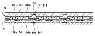
第1の研磨前基礎構造物の第1の面と第2の研磨前基礎構造物の第1の面とが対向するように、第1の研磨前基礎構造物と第2の研磨前基礎構造物とを張り合わせる工程と、
第1の研磨前基礎構造物が研磨により薄くされることによって形成された第1の基礎構造物と第2の研磨前基礎構造物が研磨により薄くされることによって形成された第2の基礎構造物との積層体が得られるように、張り合わされた状態の第1の研磨前基礎構造物と第2の研磨前基礎構造物のそれぞれの第2の面を研磨する工程とを含んでいる。
互いに反対側を向いた第1および第2の面を有する1つの半導体ウェハにおける第1の面に処理を施すことによって、複数の半導体チップ予定部が配列され、且つ半導体ウェハの第1および第2の面に対応する第1および第2の面を有する第1の基礎構造物前ウェハを作製する工程と、
互いに反対側を向いた第1および第2の面を有する1つの半導体ウェハにおける第1の面に処理を施すことによって、複数の半導体チップ予定部が配列され、且つ半導体ウェハの第1および第2の面に対応する第1および第2の面を有する第2の基礎構造物前ウェハを作製する工程と、
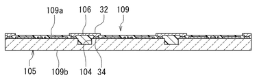
第1の基礎構造物前ウェハに対して、少なくとも1つの半導体チップ予定部に隣接するように延び、第1の基礎構造物前ウェハの第1の面において開口し、且つ溝の底部が第1の基礎構造物前ウェハの第2の面に達しない1以上の溝を形成し、1以上の溝を埋めるように、後に絶縁部の一部となる絶縁層を形成し、一部が絶縁層の上に配置されるように、複数の電極を形成して、第1の基礎構造物前ウェハの第1および第2の面に対応する第1および第2の面を有する第1の研磨前基礎構造物を作製する工程と、
第2の基礎構造物前ウェハに対して、少なくとも1つの半導体チップ予定部に隣接するように延び、第2の基礎構造物前ウェハの第1の面において開口し、且つ溝の底部が第2の基礎構造物前ウェハの第2の面に達しない1以上の溝を形成し、1以上の溝を埋めるように、後に絶縁部の一部となる絶縁層を形成し、一部が絶縁層の上に配置されるように、複数の電極を形成して、第2の基礎構造物前ウェハの第1および第2の面に対応する第1および第2の面を有する第2の研磨前基礎構造物を作製する工程と、
第1の研磨前基礎構造物の第1の面と第2の研磨前基礎構造物の第1の面とが対向するように、第1の研磨前基礎構造物と第2の研磨前基礎構造物とを張り合わせる工程と、
第1の研磨前基礎構造物が研磨により薄くされることによって形成された第1の基礎構造物と第2の研磨前基礎構造物が研磨により薄くされることによって形成された第2の基礎構造物との積層体が得られるように、張り合わされた状態の第1の研磨前基礎構造物と第2の研磨前基礎構造物のそれぞれの第2の面を研磨する工程とを含んでいる。
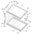
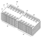
以下、本発明の実施の形態について図面を参照して詳細に説明する。始めに、図1を参照して、本発明の第1の実施の形態に係る積層チップパッケージの構成について説明する。図1は、本実施の形態に係る積層チップパッケージの斜視図である。図1に示したように、本実施の形態に係る積層チップパッケージ1は、直方体形状の本体2を備えている。本体2は、上面2a、下面2b、互いに反対側を向いた第1の側面2cおよび第2の側面2d、ならびに互いに反対側を向いた第3の側面2eおよび第4の側面2fを有している。
次に、本発明の第2の実施の形態について説明する。本実施の形態に係る積層チップパッケージ1の外観は、第1の実施の形態と同様に、図1に示したようになる。
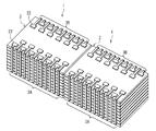
次に、本発明の第3の実施の形態について説明する。図34は、本実施の形態に係る積層チップパッケージ1の斜視図である。図34に示したように、本実施の形態に係る積層チップパッケージ1は、本体2の少なくとも1つの側面に配置された配線3として、本体2の第1の側面2cに配置された配線3Aのみを備え、第1および第2の実施の形態では本体2の第2の側面2dに配置されていた配線3B(図1参照)は備えていない。また、本実施の形態では、端子層20に含まれる複数のパッド状端子22は、全て、本体2の側面2cに配置された端面を有するものになっている。複数のパッド状端子22の端面には、配線3Aが接続されている。
Claims (15)
- 積層された複数の階層部分を備え、
前記複数の階層部分の各々は、デバイスが形成された第1の面とその反対側の第2の面とを有する半導体チップを含み、
前記複数の階層部分は、前記半導体チップの第1の面同士が対向するように配置された対の階層部分を一対以上含むことを特徴とする積層チップパッケージ。 - 上面、下面および4つの側面を有する本体と、
前記本体の少なくとも1つの側面に配置された配線とを備え、
前記本体は、積層された複数の階層部分を含み、
前記複数の階層部分の各々は、デバイスが形成された第1の面とその反対側の第2の面と4つの側面を有する半導体チップと、前記半導体チップの4つの側面のうちの少なくとも1つの側面を覆う絶縁部と、前記半導体チップに接続された複数の電極とを含み、
前記絶縁部は、前記配線が配置された前記本体の前記少なくとも1つの側面に配置された少なくとも1つの端面を有し、
前記複数の電極の各々は、前記配線が配置された前記本体の前記少なくとも1つの側面に配置され且つ前記絶縁部によって囲まれた端面を有し、
前記配線は、前記複数の階層部分における複数の電極の端面に接続され、
前記複数の階層部分は、前記半導体チップの第1の面同士が対向するように配置された対の階層部分を一対以上含むことを特徴とする積層チップパッケージ。 - 一対の階層部分は、第1の半導体チップを含む第1の階層部分と第2の半導体チップを含む第2の階層部分よりなり、
前記第1の半導体チップは、所定の順序で配列された複数の第1の端子を有し、
前記第2の半導体チップは、前記複数の第1の端子に対応して所定の順序で配列された複数の第2の端子を有し、
前記第1の階層部分は、前記複数の電極として、前記複数の第1の端子に接続された複数の第1の電極を有し、
前記第2の階層部分は、前記複数の電極として、前記複数の第2の端子に接続された複数の第2の電極を有し、
前記第1の半導体チップと第2の半導体チップの第1の面同士が対向するように前記第1の階層部分と第2の階層部分が配置された状態で同一方向から見たときに、前記複数の第2の端子の配列の順序は前記複数の第1の端子の配列の順序とは逆であり、前記本体の前記少なくとも1つの側面に配置された複数の第1の電極の端面は、対応する複数の第1の端子の配列と同じ順序で配列され、前記本体の前記少なくとも1つの側面に配置された複数の第2の電極の端面は、対応する複数の第2の端子の配列とは逆の順序で配列されていることを特徴とする請求項2記載の積層チップパッケージ。 - 積層された複数の階層部分を備え、前記複数の階層部分の各々は、デバイスが形成された第1の面とその反対側の第2の面とを有する半導体チップを含み、前記複数の階層部分は、前記半導体チップの第1の面同士が対向するように配置された対の階層部分を一対以上含む積層チップパッケージを製造する方法であって、
前記積層チップパッケージの複数の階層部分にそれぞれ対応する複数の基礎構造物であって、各々が対応する階層部分を複数含み、後にそれら対応する階層部分のうちの隣接するもの同士の境界位置で切断される複数の基礎構造物を、前記積層チップパッケージの複数の階層部分の積層の順序に対応させて積層して、積層基礎構造物を作製する工程と、
前記積層基礎構造物を用いて、複数の積層チップパッケージを作製する工程とを備え、
前記積層基礎構造物を作製する工程は、
互いに反対側を向いた第1および第2の面を有する1つの半導体ウェハにおける前記第1の面に処理を施すことによって、複数の半導体チップ予定部が配列され、且つ前記半導体ウェハの第1および第2の面に対応する第1および第2の面を有する第1の研磨前基礎構造物を作製する工程と、
互いに反対側を向いた第1および第2の面を有する1つの半導体ウェハにおける前記第1の面に処理を施すことによって、複数の半導体チップ予定部が配列され、且つ前記半導体ウェハの第1および第2の面に対応する第1および第2の面を有する第2の研磨前基礎構造物を作製する工程と、
前記第1の研磨前基礎構造物の第1の面と前記第2の研磨前基礎構造物の第1の面とが対向するように、前記第1の研磨前基礎構造物と前記第2の研磨前基礎構造物とを張り合わせる工程と、
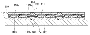
前記第1の研磨前基礎構造物が研磨により薄くされることによって形成された第1の基礎構造物と前記第2の研磨前基礎構造物が研磨により薄くされることによって形成された第2の基礎構造物との積層体が得られるように、張り合わされた状態の前記第1の研磨前基礎構造物と前記第2の研磨前基礎構造物のそれぞれの第2の面を研磨する工程とを含むことを特徴とする積層チップパッケージの製造方法。 - 前記積層基礎構造物を作製する工程は、更に、それぞれ前記第1の研磨前基礎構造物を作製する工程から前記研磨する工程までの一連の工程を経て作製された複数の積層体を張り合わせる工程を含むことを特徴とする請求項4記載の積層チップパッケージの製造方法。
- 上面、下面および4つの側面を有する本体と、
前記本体の少なくとも1つの側面に配置された配線とを備え、
前記本体は、積層された複数の階層部分を含み、
前記複数の階層部分の各々は、デバイスが形成された第1の面とその反対側の第2の面と4つの側面を有する半導体チップと、前記半導体チップの4つの側面のうちの少なくとも1つの側面を覆う絶縁部と、前記半導体チップに接続された複数の電極とを含み、
前記絶縁部は、前記配線が配置された前記本体の前記少なくとも1つの側面に配置された少なくとも1つの端面を有し、
前記複数の電極の各々は、前記配線が配置された前記本体の前記少なくとも1つの側面に配置され且つ前記絶縁部によって囲まれた端面を有し、
前記配線は、前記複数の階層部分における複数の電極の端面に接続され、
前記複数の階層部分は、前記半導体チップの第1の面同士が対向するように配置された対の階層部分を一対以上含む積層チップパッケージを製造する方法であって、
前記積層チップパッケージの複数の階層部分にそれぞれ対応する複数の基礎構造物であって、各々が対応する階層部分を複数含み、後にそれら対応する階層部分のうちの隣接するもの同士の境界位置で切断される複数の基礎構造物を、前記積層チップパッケージの複数の階層部分の積層の順序に対応させて積層して、積層基礎構造物を作製する工程と、
前記積層基礎構造物を用いて、複数の積層チップパッケージを作製する工程とを備え、
前記積層基礎構造物を作製する工程は、
互いに反対側を向いた第1および第2の面を有する1つの半導体ウェハにおける前記第1の面に処理を施すことによって、複数の半導体チップ予定部が配列され、且つ前記半導体ウェハの第1および第2の面に対応する第1および第2の面を有する第1の基礎構造物前ウェハを作製する工程と、
互いに反対側を向いた第1および第2の面を有する1つの半導体ウェハにおける前記第1の面に処理を施すことによって、複数の半導体チップ予定部が配列され、且つ前記半導体ウェハの第1および第2の面に対応する第1および第2の面を有する第2の基礎構造物前ウェハを作製する工程と、
前記第1の基礎構造物前ウェハに対して、少なくとも1つの半導体チップ予定部に隣接するように延び、前記第1の基礎構造物前ウェハの第1の面において開口し、且つ溝の底部が前記第1の基礎構造物前ウェハの第2の面に達しない1以上の溝を形成し、前記1以上の溝を埋めるように、後に前記絶縁部の一部となる絶縁層を形成し、一部が前記絶縁層の上に配置されるように、前記複数の電極を形成して、前記第1の基礎構造物前ウェハの第1および第2の面に対応する第1および第2の面を有する第1の研磨前基礎構造物を作製する工程と、
前記第2の基礎構造物前ウェハに対して、少なくとも1つの半導体チップ予定部に隣接するように延び、前記第2の基礎構造物前ウェハの第1の面において開口し、且つ溝の底部が前記第2の基礎構造物前ウェハの第2の面に達しない1以上の溝を形成し、前記1以上の溝を埋めるように、後に前記絶縁部の一部となる絶縁層を形成し、一部が前記絶縁層の上に配置されるように、前記複数の電極を形成して、前記第2の基礎構造物前ウェハの第1および第2の面に対応する第1および第2の面を有する第2の研磨前基礎構造物を作製する工程と、
前記第1の研磨前基礎構造物の第1の面と前記第2の研磨前基礎構造物の第1の面とが対向するように、前記第1の研磨前基礎構造物と前記第2の研磨前基礎構造物とを張り合わせる工程と、
前記第1の研磨前基礎構造物が研磨により薄くされることによって形成された第1の基礎構造物と前記第2の研磨前基礎構造物が研磨により薄くされることによって形成された第2の基礎構造物との積層体が得られるように、張り合わされた状態の前記第1の研磨前基礎構造物と前記第2の研磨前基礎構造物のそれぞれの第2の面を研磨する工程とを含むことを特徴とする積層チップパッケージの製造方法。 - 一対の階層部分は、第1の半導体チップを含む第1の階層部分と第2の半導体チップを含む第2の階層部分よりなり、
前記第1の半導体チップは、所定の順序で配列された複数の第1の端子を有し、
前記第2の半導体チップは、前記複数の第1の端子に対応して所定の順序で配列された複数の第2の端子を有し、
前記第1の階層部分は、前記複数の電極として、前記複数の第1の端子に接続された複数の第1の電極を有し、
前記第2の階層部分は、前記複数の電極として、前記複数の第2の端子に接続された複数の第2の電極を有し、
前記第1の半導体チップと第2の半導体チップの第1の面同士が対向するように前記第1の階層部分と第2の階層部分が配置された状態で同一方向から見たときに、前記複数の第2の端子の配列の順序は前記複数の第1の端子の配列の順序とは逆であり、前記本体の前記少なくとも1つの側面に配置された複数の第1の電極の端面は、対応する複数の第1の端子の配列と同じ順序で配列され、前記本体の前記少なくとも1つの側面に配置された複数の第2の電極の端面は、対応する複数の第2の端子の配列とは逆の順序で配列されることを特徴とする請求項6記載の積層チップパッケージの製造方法。 - 前記研磨する工程では、前記第1の研磨前基礎構造物における1以上の溝が露出するまで前記第1の研磨前基礎構造物の第2の面を研磨し、前記第2の研磨前基礎構造物における1以上の溝が露出するまで前記第2の研磨前基礎構造物の第2の面を研磨することを特徴とする請求項6記載の積層チップパッケージの製造方法。
- 前記積層基礎構造物を作製する工程は、更に、それぞれ前記第1の基礎構造物前ウェハを作製する工程から前記研磨する工程までの一連の工程を経て作製された複数の積層体を張り合わせる工程を含むことを特徴とする請求項6記載の積層チップパッケージの製造方法。
- 前記第1の研磨前基礎構造物を作製する工程と前記第2の研磨前基礎構造物を作製する工程では、それぞれ、前記複数の電極の形成と同時に、前記絶縁層の上にアライメントマークを形成し、
前記複数の積層体を張り合わせる工程では、前記アライメントマークを利用して、前記複数の積層体の位置合わせを行うことを特徴とする請求項9記載の積層チップパッケージの製造方法。 - 前記絶縁層は透明であることを特徴とする請求項10記載の積層チップパッケージの製造方法。
- 前記複数の積層チップパッケージを作製する工程は、
前記積層基礎構造物を切断することによって、前記複数の階層部分の積層方向と直交する一方向に配列され、それぞれ後に前記本体となる複数の本体予定部を含む本体集合体を作製する工程と、
前記本体集合体における各本体予定部に対してそれぞれ前記配線を形成する工程と、
前記配線の形成後、複数の本体予定部が互いに分離されてそれぞれ前記本体となることによって複数の前記積層チップパッケージが形成されるように、前記本体集合体を切断する工程とを含み、
前記本体集合体を作製する工程において、前記溝が延びる方向に沿って切断面が形成されるように前記絶縁層を切断し、これにより、前記絶縁層の前記切断面によって前記絶縁部の前記少なくとも1つの端面の一部が形成され、且つ前記複数の電極の端面が露出することを特徴とする請求項6記載の積層チップパッケージの製造方法。 - 前記配線を形成する工程では、複数の前記本体集合体を、前記複数の階層部分の積層方向に並べた後、この複数の本体集合体における各本体予定部に対してそれぞれ前記配線を形成することを特徴とする請求項12記載の積層チップパッケージの製造方法。
- 前記第1の研磨前基礎構造物を作製する工程と前記第2の研磨前基礎構造物を作製する工程では、それぞれ、前記複数の電極の形成と同時に、前記絶縁層の上にアライメントマークを形成し、
前記配線を形成する工程では、前記アライメントマークを利用して、前記複数の階層部分の積層方向に並べる前記複数の本体集合体の位置合わせを行うことを特徴とする請求項13記載の積層チップパッケージの製造方法。 - 前記絶縁層は透明であることを特徴とする請求項14記載の積層チップパッケージの製造方法。
Applications Claiming Priority (2)
| Application Number | Priority Date | Filing Date | Title |
|---|---|---|---|
| US12/216,143 US7868442B2 (en) | 2008-06-30 | 2008-06-30 | Layered chip package and method of manufacturing same |
| US12/216,143 | 2008-06-30 |
Related Child Applications (1)
| Application Number | Title | Priority Date | Filing Date |
|---|---|---|---|
| JP2013089040A Division JP5576962B2 (ja) | 2008-06-30 | 2013-04-22 | 積層チップパッケージの製造方法 |
Publications (2)
| Publication Number | Publication Date |
|---|---|
| JP2010016374A true JP2010016374A (ja) | 2010-01-21 |
| JP5275915B2 JP5275915B2 (ja) | 2013-08-28 |
Family
ID=41446418
Family Applications (2)
| Application Number | Title | Priority Date | Filing Date |
|---|---|---|---|
| JP2009148254A Expired - Fee Related JP5275915B2 (ja) | 2008-06-30 | 2009-06-23 | 積層チップパッケージ |
| JP2013089040A Expired - Fee Related JP5576962B2 (ja) | 2008-06-30 | 2013-04-22 | 積層チップパッケージの製造方法 |
Family Applications After (1)
| Application Number | Title | Priority Date | Filing Date |
|---|---|---|---|
| JP2013089040A Expired - Fee Related JP5576962B2 (ja) | 2008-06-30 | 2013-04-22 | 積層チップパッケージの製造方法 |
Country Status (2)
| Country | Link |
|---|---|
| US (2) | US7868442B2 (ja) |
| JP (2) | JP5275915B2 (ja) |
Cited By (2)
| Publication number | Priority date | Publication date | Assignee | Title |
|---|---|---|---|---|
| JP2011071441A (ja) * | 2009-09-28 | 2011-04-07 | Rohm Co Ltd | 半導体装置の製造方法、半導体装置およびウエハ積層構造物 |
| JP2012256844A (ja) * | 2011-06-09 | 2012-12-27 | Headway Technologies Inc | 積層チップパッケージおよびその製造方法 |
Families Citing this family (230)
| Publication number | Priority date | Publication date | Assignee | Title |
|---|---|---|---|---|
| US7968374B2 (en) * | 2009-02-06 | 2011-06-28 | Headway Technologies, Inc. | Layered chip package with wiring on the side surfaces |
| US20110031997A1 (en) * | 2009-04-14 | 2011-02-10 | NuPGA Corporation | Method for fabrication of a semiconductor device and structure |
| US8754533B2 (en) * | 2009-04-14 | 2014-06-17 | Monolithic 3D Inc. | Monolithic three-dimensional semiconductor device and structure |
| US8362482B2 (en) | 2009-04-14 | 2013-01-29 | Monolithic 3D Inc. | Semiconductor device and structure |
| US9577642B2 (en) | 2009-04-14 | 2017-02-21 | Monolithic 3D Inc. | Method to form a 3D semiconductor device |
| US8058137B1 (en) | 2009-04-14 | 2011-11-15 | Monolithic 3D Inc. | Method for fabrication of a semiconductor device and structure |
| US8395191B2 (en) | 2009-10-12 | 2013-03-12 | Monolithic 3D Inc. | Semiconductor device and structure |
| US8669778B1 (en) | 2009-04-14 | 2014-03-11 | Monolithic 3D Inc. | Method for design and manufacturing of a 3D semiconductor device |
| US9509313B2 (en) | 2009-04-14 | 2016-11-29 | Monolithic 3D Inc. | 3D semiconductor device |
| US20110199116A1 (en) * | 2010-02-16 | 2011-08-18 | NuPGA Corporation | Method for fabrication of a semiconductor device and structure |
| US10388863B2 (en) | 2009-10-12 | 2019-08-20 | Monolithic 3D Inc. | 3D memory device and structure |
| US10043781B2 (en) | 2009-10-12 | 2018-08-07 | Monolithic 3D Inc. | 3D semiconductor device and structure |
| US11018133B2 (en) | 2009-10-12 | 2021-05-25 | Monolithic 3D Inc. | 3D integrated circuit |
| US10910364B2 (en) | 2009-10-12 | 2021-02-02 | Monolitaic 3D Inc. | 3D semiconductor device |
| US10366970B2 (en) | 2009-10-12 | 2019-07-30 | Monolithic 3D Inc. | 3D semiconductor device and structure |
| US11984445B2 (en) | 2009-10-12 | 2024-05-14 | Monolithic 3D Inc. | 3D semiconductor devices and structures with metal layers |
| US10157909B2 (en) | 2009-10-12 | 2018-12-18 | Monolithic 3D Inc. | 3D semiconductor device and structure |
| US11374118B2 (en) | 2009-10-12 | 2022-06-28 | Monolithic 3D Inc. | Method to form a 3D integrated circuit |
| US9099424B1 (en) | 2012-08-10 | 2015-08-04 | Monolithic 3D Inc. | Semiconductor system, device and structure with heat removal |
| US8742476B1 (en) | 2012-11-27 | 2014-06-03 | Monolithic 3D Inc. | Semiconductor device and structure |
| US10354995B2 (en) | 2009-10-12 | 2019-07-16 | Monolithic 3D Inc. | Semiconductor memory device and structure |
| US12027518B1 (en) | 2009-10-12 | 2024-07-02 | Monolithic 3D Inc. | 3D semiconductor devices and structures with metal layers |
| US8012802B2 (en) * | 2010-02-04 | 2011-09-06 | Headway Technologies, Inc. | Method of manufacturing layered chip package |
| US8461035B1 (en) | 2010-09-30 | 2013-06-11 | Monolithic 3D Inc. | Method for fabrication of a semiconductor device and structure |
| US8026521B1 (en) | 2010-10-11 | 2011-09-27 | Monolithic 3D Inc. | Semiconductor device and structure |
| US9099526B2 (en) | 2010-02-16 | 2015-08-04 | Monolithic 3D Inc. | Integrated circuit device and structure |
| US8492886B2 (en) | 2010-02-16 | 2013-07-23 | Monolithic 3D Inc | 3D integrated circuit with logic |
| US8441106B2 (en) * | 2010-02-18 | 2013-05-14 | Seagate Technology Llc | Apparatus and method for defining laser cleave alignment |
| US10217667B2 (en) | 2011-06-28 | 2019-02-26 | Monolithic 3D Inc. | 3D semiconductor device, fabrication method and system |
| US9953925B2 (en) | 2011-06-28 | 2018-04-24 | Monolithic 3D Inc. | Semiconductor system and device |
| US8901613B2 (en) | 2011-03-06 | 2014-12-02 | Monolithic 3D Inc. | Semiconductor device and structure for heat removal |
| US9219005B2 (en) | 2011-06-28 | 2015-12-22 | Monolithic 3D Inc. | Semiconductor system and device |
| US8541887B2 (en) | 2010-09-03 | 2013-09-24 | Headway Technologies, Inc. | Layered chip package and method of manufacturing same |
| US8441112B2 (en) | 2010-10-01 | 2013-05-14 | Headway Technologies, Inc. | Method of manufacturing layered chip package |
| US12362219B2 (en) | 2010-11-18 | 2025-07-15 | Monolithic 3D Inc. | 3D semiconductor memory device and structure |
| US10497713B2 (en) | 2010-11-18 | 2019-12-03 | Monolithic 3D Inc. | 3D semiconductor memory device and structure |
| US8163581B1 (en) | 2010-10-13 | 2012-04-24 | Monolith IC 3D | Semiconductor and optoelectronic devices |
| US8273610B2 (en) | 2010-11-18 | 2012-09-25 | Monolithic 3D Inc. | Method of constructing a semiconductor device and structure |
| US11482440B2 (en) | 2010-12-16 | 2022-10-25 | Monolithic 3D Inc. | 3D semiconductor device and structure with a built-in test circuit for repairing faulty circuits |
| US11315980B1 (en) | 2010-10-11 | 2022-04-26 | Monolithic 3D Inc. | 3D semiconductor device and structure with transistors |
| US10290682B2 (en) | 2010-10-11 | 2019-05-14 | Monolithic 3D Inc. | 3D IC semiconductor device and structure with stacked memory |
| US11158674B2 (en) | 2010-10-11 | 2021-10-26 | Monolithic 3D Inc. | Method to produce a 3D semiconductor device and structure |
| US11600667B1 (en) | 2010-10-11 | 2023-03-07 | Monolithic 3D Inc. | Method to produce 3D semiconductor devices and structures with memory |
| US10896931B1 (en) | 2010-10-11 | 2021-01-19 | Monolithic 3D Inc. | 3D semiconductor device and structure |
| US11018191B1 (en) | 2010-10-11 | 2021-05-25 | Monolithic 3D Inc. | 3D semiconductor device and structure |
| US11257867B1 (en) | 2010-10-11 | 2022-02-22 | Monolithic 3D Inc. | 3D semiconductor device and structure with oxide bonds |
| US11024673B1 (en) | 2010-10-11 | 2021-06-01 | Monolithic 3D Inc. | 3D semiconductor device and structure |
| US11227897B2 (en) | 2010-10-11 | 2022-01-18 | Monolithic 3D Inc. | Method for producing a 3D semiconductor memory device and structure |
| US11469271B2 (en) | 2010-10-11 | 2022-10-11 | Monolithic 3D Inc. | Method to produce 3D semiconductor devices and structures with memory |
| US8618646B2 (en) | 2010-10-12 | 2013-12-31 | Headway Technologies, Inc. | Layered chip package and method of manufacturing same |
| US11869915B2 (en) | 2010-10-13 | 2024-01-09 | Monolithic 3D Inc. | Multilevel semiconductor device and structure with image sensors and wafer bonding |
| US11437368B2 (en) | 2010-10-13 | 2022-09-06 | Monolithic 3D Inc. | Multilevel semiconductor device and structure with oxide bonding |
| US11063071B1 (en) | 2010-10-13 | 2021-07-13 | Monolithic 3D Inc. | Multilevel semiconductor device and structure with waveguides |
| US11404466B2 (en) | 2010-10-13 | 2022-08-02 | Monolithic 3D Inc. | Multilevel semiconductor device and structure with image sensors |
| US11694922B2 (en) | 2010-10-13 | 2023-07-04 | Monolithic 3D Inc. | Multilevel semiconductor device and structure with oxide bonding |
| US12094892B2 (en) | 2010-10-13 | 2024-09-17 | Monolithic 3D Inc. | 3D micro display device and structure |
| US12360310B2 (en) | 2010-10-13 | 2025-07-15 | Monolithic 3D Inc. | Multilevel semiconductor device and structure with oxide bonding |
| US12080743B2 (en) | 2010-10-13 | 2024-09-03 | Monolithic 3D Inc. | Multilevel semiconductor device and structure with image sensors and wafer bonding |
| US11929372B2 (en) | 2010-10-13 | 2024-03-12 | Monolithic 3D Inc. | Multilevel semiconductor device and structure with image sensors and wafer bonding |
| US10978501B1 (en) | 2010-10-13 | 2021-04-13 | Monolithic 3D Inc. | Multilevel semiconductor device and structure with waveguides |
| US11605663B2 (en) | 2010-10-13 | 2023-03-14 | Monolithic 3D Inc. | Multilevel semiconductor device and structure with image sensors and wafer bonding |
| US9197804B1 (en) | 2011-10-14 | 2015-11-24 | Monolithic 3D Inc. | Semiconductor and optoelectronic devices |
| US11984438B2 (en) | 2010-10-13 | 2024-05-14 | Monolithic 3D Inc. | Multilevel semiconductor device and structure with oxide bonding |
| US10998374B1 (en) | 2010-10-13 | 2021-05-04 | Monolithic 3D Inc. | Multilevel semiconductor device and structure |
| US11043523B1 (en) | 2010-10-13 | 2021-06-22 | Monolithic 3D Inc. | Multilevel semiconductor device and structure with image sensors |
| US11327227B2 (en) | 2010-10-13 | 2022-05-10 | Monolithic 3D Inc. | Multilevel semiconductor device and structure with electromagnetic modulators |
| US10679977B2 (en) | 2010-10-13 | 2020-06-09 | Monolithic 3D Inc. | 3D microdisplay device and structure |
| US11133344B2 (en) | 2010-10-13 | 2021-09-28 | Monolithic 3D Inc. | Multilevel semiconductor device and structure with image sensors |
| US10943934B2 (en) | 2010-10-13 | 2021-03-09 | Monolithic 3D Inc. | Multilevel semiconductor device and structure |
| US10833108B2 (en) | 2010-10-13 | 2020-11-10 | Monolithic 3D Inc. | 3D microdisplay device and structure |
| US11164898B2 (en) | 2010-10-13 | 2021-11-02 | Monolithic 3D Inc. | Multilevel semiconductor device and structure |
| US11163112B2 (en) | 2010-10-13 | 2021-11-02 | Monolithic 3D Inc. | Multilevel semiconductor device and structure with electromagnetic modulators |
| US11855114B2 (en) | 2010-10-13 | 2023-12-26 | Monolithic 3D Inc. | Multilevel semiconductor device and structure with image sensors and wafer bonding |
| US11855100B2 (en) | 2010-10-13 | 2023-12-26 | Monolithic 3D Inc. | Multilevel semiconductor device and structure with oxide bonding |
| US11784082B2 (en) | 2010-11-18 | 2023-10-10 | Monolithic 3D Inc. | 3D semiconductor device and structure with bonding |
| US11482438B2 (en) | 2010-11-18 | 2022-10-25 | Monolithic 3D Inc. | Methods for producing a 3D semiconductor memory device and structure |
| US11164770B1 (en) | 2010-11-18 | 2021-11-02 | Monolithic 3D Inc. | Method for producing a 3D semiconductor memory device and structure |
| US12125737B1 (en) | 2010-11-18 | 2024-10-22 | Monolithic 3D Inc. | 3D semiconductor device and structure with metal layers and memory cells |
| US11355380B2 (en) | 2010-11-18 | 2022-06-07 | Monolithic 3D Inc. | Methods for producing 3D semiconductor memory device and structure utilizing alignment marks |
| US11862503B2 (en) | 2010-11-18 | 2024-01-02 | Monolithic 3D Inc. | Method for producing a 3D semiconductor device and structure with memory cells and multiple metal layers |
| US11569117B2 (en) | 2010-11-18 | 2023-01-31 | Monolithic 3D Inc. | 3D semiconductor device and structure with single-crystal layers |
| US11107721B2 (en) | 2010-11-18 | 2021-08-31 | Monolithic 3D Inc. | 3D semiconductor device and structure with NAND logic |
| US11031275B2 (en) | 2010-11-18 | 2021-06-08 | Monolithic 3D Inc. | 3D semiconductor device and structure with memory |
| US12154817B1 (en) | 2010-11-18 | 2024-11-26 | Monolithic 3D Inc. | Methods for producing a 3D semiconductor memory device and structure |
| US11018042B1 (en) | 2010-11-18 | 2021-05-25 | Monolithic 3D Inc. | 3D semiconductor memory device and structure |
| US11355381B2 (en) | 2010-11-18 | 2022-06-07 | Monolithic 3D Inc. | 3D semiconductor memory device and structure |
| US11615977B2 (en) | 2010-11-18 | 2023-03-28 | Monolithic 3D Inc. | 3D semiconductor memory device and structure |
| US12243765B2 (en) | 2010-11-18 | 2025-03-04 | Monolithic 3D Inc. | 3D semiconductor device and structure with metal layers and memory cells |
| US12272586B2 (en) | 2010-11-18 | 2025-04-08 | Monolithic 3D Inc. | 3D semiconductor memory device and structure with memory and metal layers |
| US11804396B2 (en) | 2010-11-18 | 2023-10-31 | Monolithic 3D Inc. | Methods for producing a 3D semiconductor device and structure with memory cells and multiple metal layers |
| US11610802B2 (en) | 2010-11-18 | 2023-03-21 | Monolithic 3D Inc. | Method for producing a 3D semiconductor device and structure with single crystal transistors and metal gate electrodes |
| US11211279B2 (en) | 2010-11-18 | 2021-12-28 | Monolithic 3D Inc. | Method for processing a 3D integrated circuit and structure |
| US11482439B2 (en) | 2010-11-18 | 2022-10-25 | Monolithic 3D Inc. | Methods for producing a 3D semiconductor memory device comprising charge trap junction-less transistors |
| US12100611B2 (en) | 2010-11-18 | 2024-09-24 | Monolithic 3D Inc. | Methods for producing a 3D semiconductor device and structure with memory cells and multiple metal layers |
| US11121021B2 (en) | 2010-11-18 | 2021-09-14 | Monolithic 3D Inc. | 3D semiconductor device and structure |
| US11508605B2 (en) | 2010-11-18 | 2022-11-22 | Monolithic 3D Inc. | 3D semiconductor memory device and structure |
| US11923230B1 (en) | 2010-11-18 | 2024-03-05 | Monolithic 3D Inc. | 3D semiconductor device and structure with bonding |
| US12144190B2 (en) | 2010-11-18 | 2024-11-12 | Monolithic 3D Inc. | 3D semiconductor device and structure with bonding and memory cells preliminary class |
| US11094576B1 (en) | 2010-11-18 | 2021-08-17 | Monolithic 3D Inc. | Methods for producing a 3D semiconductor memory device and structure |
| US11495484B2 (en) | 2010-11-18 | 2022-11-08 | Monolithic 3D Inc. | 3D semiconductor devices and structures with at least two single-crystal layers |
| US12033884B2 (en) | 2010-11-18 | 2024-07-09 | Monolithic 3D Inc. | Methods for producing a 3D semiconductor device and structure with memory cells and multiple metal layers |
| US11901210B2 (en) | 2010-11-18 | 2024-02-13 | Monolithic 3D Inc. | 3D semiconductor device and structure with memory |
| US11521888B2 (en) | 2010-11-18 | 2022-12-06 | Monolithic 3D Inc. | 3D semiconductor device and structure with high-k metal gate transistors |
| US11735462B2 (en) | 2010-11-18 | 2023-08-22 | Monolithic 3D Inc. | 3D semiconductor device and structure with single-crystal layers |
| US11004719B1 (en) | 2010-11-18 | 2021-05-11 | Monolithic 3D Inc. | Methods for producing a 3D semiconductor memory device and structure |
| US11443971B2 (en) | 2010-11-18 | 2022-09-13 | Monolithic 3D Inc. | 3D semiconductor device and structure with memory |
| US11854857B1 (en) | 2010-11-18 | 2023-12-26 | Monolithic 3D Inc. | Methods for producing a 3D semiconductor device and structure with memory cells and multiple metal layers |
| US12136562B2 (en) | 2010-11-18 | 2024-11-05 | Monolithic 3D Inc. | 3D semiconductor device and structure with single-crystal layers |
| US12068187B2 (en) | 2010-11-18 | 2024-08-20 | Monolithic 3D Inc. | 3D semiconductor device and structure with bonding and DRAM memory cells |
| US12463076B2 (en) | 2010-12-16 | 2025-11-04 | Monolithic 3D Inc. | 3D semiconductor device and structure |
| US8975670B2 (en) | 2011-03-06 | 2015-03-10 | Monolithic 3D Inc. | Semiconductor device and structure for heat removal |
| US8358015B2 (en) | 2011-06-09 | 2013-01-22 | Headway Technologies, Inc. | Layered chip package and method of manufacturing same |
| US10388568B2 (en) | 2011-06-28 | 2019-08-20 | Monolithic 3D Inc. | 3D semiconductor device and system |
| US8426981B2 (en) * | 2011-09-22 | 2013-04-23 | Headway Technologies, Inc. | Composite layered chip package |
| US8687399B2 (en) | 2011-10-02 | 2014-04-01 | Monolithic 3D Inc. | Semiconductor device and structure |
| US9029173B2 (en) | 2011-10-18 | 2015-05-12 | Monolithic 3D Inc. | Method for fabrication of a semiconductor device and structure |
| US8492175B1 (en) * | 2011-11-28 | 2013-07-23 | Applied Micro Circuits Corporation | System and method for aligning surface mount devices on a substrate |
| US9000557B2 (en) * | 2012-03-17 | 2015-04-07 | Zvi Or-Bach | Semiconductor device and structure |
| US11694944B1 (en) | 2012-04-09 | 2023-07-04 | Monolithic 3D Inc. | 3D semiconductor device and structure with metal layers and a connective path |
| US11735501B1 (en) | 2012-04-09 | 2023-08-22 | Monolithic 3D Inc. | 3D semiconductor device and structure with metal layers and a connective path |
| US11164811B2 (en) | 2012-04-09 | 2021-11-02 | Monolithic 3D Inc. | 3D semiconductor device with isolation layers and oxide-to-oxide bonding |
| US11088050B2 (en) | 2012-04-09 | 2021-08-10 | Monolithic 3D Inc. | 3D semiconductor device with isolation layers |
| US11410912B2 (en) | 2012-04-09 | 2022-08-09 | Monolithic 3D Inc. | 3D semiconductor device with vias and isolation layers |
| US11616004B1 (en) | 2012-04-09 | 2023-03-28 | Monolithic 3D Inc. | 3D semiconductor device and structure with metal layers and a connective path |
| US11476181B1 (en) | 2012-04-09 | 2022-10-18 | Monolithic 3D Inc. | 3D semiconductor device and structure with metal layers |
| US8557632B1 (en) | 2012-04-09 | 2013-10-15 | Monolithic 3D Inc. | Method for fabrication of a semiconductor device and structure |
| US11881443B2 (en) | 2012-04-09 | 2024-01-23 | Monolithic 3D Inc. | 3D semiconductor device and structure with metal layers and a connective path |
| US11594473B2 (en) | 2012-04-09 | 2023-02-28 | Monolithic 3D Inc. | 3D semiconductor device and structure with metal layers and a connective path |
| US10600888B2 (en) | 2012-04-09 | 2020-03-24 | Monolithic 3D Inc. | 3D semiconductor device |
| US8686428B1 (en) | 2012-11-16 | 2014-04-01 | Monolithic 3D Inc. | Semiconductor device and structure |
| US11309292B2 (en) | 2012-12-22 | 2022-04-19 | Monolithic 3D Inc. | 3D semiconductor device and structure with metal layers |
| US8674470B1 (en) | 2012-12-22 | 2014-03-18 | Monolithic 3D Inc. | Semiconductor device and structure |
| US11063024B1 (en) | 2012-12-22 | 2021-07-13 | Monlithic 3D Inc. | Method to form a 3D semiconductor device and structure |
| US11217565B2 (en) | 2012-12-22 | 2022-01-04 | Monolithic 3D Inc. | Method to form a 3D semiconductor device and structure |
| US11784169B2 (en) | 2012-12-22 | 2023-10-10 | Monolithic 3D Inc. | 3D semiconductor device and structure with metal layers |
| US11018116B2 (en) | 2012-12-22 | 2021-05-25 | Monolithic 3D Inc. | Method to form a 3D semiconductor device and structure |
| US11967583B2 (en) | 2012-12-22 | 2024-04-23 | Monolithic 3D Inc. | 3D semiconductor device and structure with metal layers |
| US11916045B2 (en) | 2012-12-22 | 2024-02-27 | Monolithic 3D Inc. | 3D semiconductor device and structure with metal layers |
| US11961827B1 (en) | 2012-12-22 | 2024-04-16 | Monolithic 3D Inc. | 3D semiconductor device and structure with metal layers |
| US12051674B2 (en) | 2012-12-22 | 2024-07-30 | Monolithic 3D Inc. | 3D semiconductor device and structure with metal layers |
| US12249538B2 (en) | 2012-12-29 | 2025-03-11 | Monolithic 3D Inc. | 3D semiconductor device and structure including power distribution grids |
| US9385058B1 (en) | 2012-12-29 | 2016-07-05 | Monolithic 3D Inc. | Semiconductor device and structure |
| US11004694B1 (en) | 2012-12-29 | 2021-05-11 | Monolithic 3D Inc. | 3D semiconductor device and structure |
| US11087995B1 (en) | 2012-12-29 | 2021-08-10 | Monolithic 3D Inc. | 3D semiconductor device and structure |
| US10651054B2 (en) | 2012-12-29 | 2020-05-12 | Monolithic 3D Inc. | 3D semiconductor device and structure |
| US10892169B2 (en) | 2012-12-29 | 2021-01-12 | Monolithic 3D Inc. | 3D semiconductor device and structure |
| US9871034B1 (en) | 2012-12-29 | 2018-01-16 | Monolithic 3D Inc. | Semiconductor device and structure |
| US11430667B2 (en) | 2012-12-29 | 2022-08-30 | Monolithic 3D Inc. | 3D semiconductor device and structure with bonding |
| US11430668B2 (en) | 2012-12-29 | 2022-08-30 | Monolithic 3D Inc. | 3D semiconductor device and structure with bonding |
| US11177140B2 (en) | 2012-12-29 | 2021-11-16 | Monolithic 3D Inc. | 3D semiconductor device and structure |
| US10600657B2 (en) | 2012-12-29 | 2020-03-24 | Monolithic 3D Inc | 3D semiconductor device and structure |
| US10903089B1 (en) | 2012-12-29 | 2021-01-26 | Monolithic 3D Inc. | 3D semiconductor device and structure |
| US10115663B2 (en) | 2012-12-29 | 2018-10-30 | Monolithic 3D Inc. | 3D semiconductor device and structure |
| US11935949B1 (en) | 2013-03-11 | 2024-03-19 | Monolithic 3D Inc. | 3D semiconductor device and structure with metal layers and memory cells |
| US10325651B2 (en) | 2013-03-11 | 2019-06-18 | Monolithic 3D Inc. | 3D semiconductor device with stacked memory |
| US8902663B1 (en) | 2013-03-11 | 2014-12-02 | Monolithic 3D Inc. | Method of maintaining a memory state |
| US11869965B2 (en) | 2013-03-11 | 2024-01-09 | Monolithic 3D Inc. | 3D semiconductor device and structure with metal layers and memory cells |
| US12094965B2 (en) | 2013-03-11 | 2024-09-17 | Monolithic 3D Inc. | 3D semiconductor device and structure with metal layers and memory cells |
| US10840239B2 (en) | 2014-08-26 | 2020-11-17 | Monolithic 3D Inc. | 3D semiconductor device and structure |
| US8994404B1 (en) | 2013-03-12 | 2015-03-31 | Monolithic 3D Inc. | Semiconductor device and structure |
| US12100646B2 (en) | 2013-03-12 | 2024-09-24 | Monolithic 3D Inc. | 3D semiconductor device and structure with metal layers |
| US11923374B2 (en) | 2013-03-12 | 2024-03-05 | Monolithic 3D Inc. | 3D semiconductor device and structure with metal layers |
| US11088130B2 (en) | 2014-01-28 | 2021-08-10 | Monolithic 3D Inc. | 3D semiconductor device and structure |
| US11398569B2 (en) | 2013-03-12 | 2022-07-26 | Monolithic 3D Inc. | 3D semiconductor device and structure |
| US9117749B1 (en) | 2013-03-15 | 2015-08-25 | Monolithic 3D Inc. | Semiconductor device and structure |
| US10224279B2 (en) | 2013-03-15 | 2019-03-05 | Monolithic 3D Inc. | Semiconductor device and structure |
| US11341309B1 (en) | 2013-04-15 | 2022-05-24 | Monolithic 3D Inc. | Automation for monolithic 3D devices |
| US9021414B1 (en) | 2013-04-15 | 2015-04-28 | Monolithic 3D Inc. | Automation for monolithic 3D devices |
| US11720736B2 (en) | 2013-04-15 | 2023-08-08 | Monolithic 3D Inc. | Automation methods for 3D integrated circuits and devices |
| US11270055B1 (en) | 2013-04-15 | 2022-03-08 | Monolithic 3D Inc. | Automation for monolithic 3D devices |
| US11030371B2 (en) | 2013-04-15 | 2021-06-08 | Monolithic 3D Inc. | Automation for monolithic 3D devices |
| US11574109B1 (en) | 2013-04-15 | 2023-02-07 | Monolithic 3D Inc | Automation methods for 3D integrated circuits and devices |
| US11487928B2 (en) | 2013-04-15 | 2022-11-01 | Monolithic 3D Inc. | Automation for monolithic 3D devices |
| JP6300301B2 (ja) * | 2013-11-20 | 2018-03-28 | ローム株式会社 | 半導体装置および半導体装置の製造方法 |
| US10297586B2 (en) | 2015-03-09 | 2019-05-21 | Monolithic 3D Inc. | Methods for processing a 3D semiconductor device |
| US11031394B1 (en) | 2014-01-28 | 2021-06-08 | Monolithic 3D Inc. | 3D semiconductor device and structure |
| US11107808B1 (en) | 2014-01-28 | 2021-08-31 | Monolithic 3D Inc. | 3D semiconductor device and structure |
| US12094829B2 (en) | 2014-01-28 | 2024-09-17 | Monolithic 3D Inc. | 3D semiconductor device and structure |
| US9936580B1 (en) | 2015-01-14 | 2018-04-03 | Vlt, Inc. | Method of forming an electrical connection to an electronic module |
| US9967984B1 (en) | 2015-01-14 | 2018-05-08 | Vlt, Inc. | Power adapter packaging |
| US12477752B2 (en) | 2015-09-21 | 2025-11-18 | Monolithic 3D Inc. | 3D semiconductor memory devices and structures |
| US11937422B2 (en) | 2015-11-07 | 2024-03-19 | Monolithic 3D Inc. | Semiconductor memory device and structure |
| US10381328B2 (en) | 2015-04-19 | 2019-08-13 | Monolithic 3D Inc. | Semiconductor device and structure |
| US11056468B1 (en) * | 2015-04-19 | 2021-07-06 | Monolithic 3D Inc. | 3D semiconductor device and structure |
| US10825779B2 (en) | 2015-04-19 | 2020-11-03 | Monolithic 3D Inc. | 3D semiconductor device and structure |
| US11978731B2 (en) | 2015-09-21 | 2024-05-07 | Monolithic 3D Inc. | Method to produce a multi-level semiconductor memory device and structure |
| US11011507B1 (en) | 2015-04-19 | 2021-05-18 | Monolithic 3D Inc. | 3D semiconductor device and structure |
| US11114427B2 (en) | 2015-11-07 | 2021-09-07 | Monolithic 3D Inc. | 3D semiconductor processor and memory device and structure |
| US10264664B1 (en) * | 2015-06-04 | 2019-04-16 | Vlt, Inc. | Method of electrically interconnecting circuit assemblies |
| US11956952B2 (en) | 2015-08-23 | 2024-04-09 | Monolithic 3D Inc. | Semiconductor memory device and structure |
| US12100658B2 (en) | 2015-09-21 | 2024-09-24 | Monolithic 3D Inc. | Method to produce a 3D multilayer semiconductor device and structure |
| CN115942752A (zh) | 2015-09-21 | 2023-04-07 | 莫诺利特斯3D有限公司 | 3d半导体器件和结构 |
| US12250830B2 (en) | 2015-09-21 | 2025-03-11 | Monolithic 3D Inc. | 3D semiconductor memory devices and structures |
| US12178055B2 (en) | 2015-09-21 | 2024-12-24 | Monolithic 3D Inc. | 3D semiconductor memory devices and structures |
| US10522225B1 (en) | 2015-10-02 | 2019-12-31 | Monolithic 3D Inc. | Semiconductor device with non-volatile memory |
| US12219769B2 (en) | 2015-10-24 | 2025-02-04 | Monolithic 3D Inc. | 3D semiconductor device and structure with logic and memory |
| US11296115B1 (en) | 2015-10-24 | 2022-04-05 | Monolithic 3D Inc. | 3D semiconductor device and structure |
| US12016181B2 (en) | 2015-10-24 | 2024-06-18 | Monolithic 3D Inc. | 3D semiconductor device and structure with logic and memory |
| US12035531B2 (en) | 2015-10-24 | 2024-07-09 | Monolithic 3D Inc. | 3D semiconductor device and structure with logic and memory |
| US11114464B2 (en) | 2015-10-24 | 2021-09-07 | Monolithic 3D Inc. | 3D semiconductor device and structure |
| US10418369B2 (en) | 2015-10-24 | 2019-09-17 | Monolithic 3D Inc. | Multi-level semiconductor memory device and structure |
| US10847540B2 (en) | 2015-10-24 | 2020-11-24 | Monolithic 3D Inc. | 3D semiconductor memory device and structure |
| US12120880B1 (en) | 2015-10-24 | 2024-10-15 | Monolithic 3D Inc. | 3D semiconductor device and structure with logic and memory |
| US11991884B1 (en) | 2015-10-24 | 2024-05-21 | Monolithic 3D Inc. | 3D semiconductor device and structure with logic and memory |
| US10903734B1 (en) | 2016-04-05 | 2021-01-26 | Vicor Corporation | Delivering power to semiconductor loads |
| US11336167B1 (en) | 2016-04-05 | 2022-05-17 | Vicor Corporation | Delivering power to semiconductor loads |
| US10158357B1 (en) | 2016-04-05 | 2018-12-18 | Vlt, Inc. | Method and apparatus for delivering power to semiconductors |
| US11711928B2 (en) | 2016-10-10 | 2023-07-25 | Monolithic 3D Inc. | 3D memory devices and structures with control circuits |
| US11812620B2 (en) | 2016-10-10 | 2023-11-07 | Monolithic 3D Inc. | 3D DRAM memory devices and structures with control circuits |
| US12225704B2 (en) | 2016-10-10 | 2025-02-11 | Monolithic 3D Inc. | 3D memory devices and structures with memory arrays and metal layers |
| US11869591B2 (en) | 2016-10-10 | 2024-01-09 | Monolithic 3D Inc. | 3D memory devices and structures with control circuits |
| US11930648B1 (en) | 2016-10-10 | 2024-03-12 | Monolithic 3D Inc. | 3D memory devices and structures with metal layers |
| US11329059B1 (en) | 2016-10-10 | 2022-05-10 | Monolithic 3D Inc. | 3D memory devices and structures with thinned single crystal substrates |
| US11251149B2 (en) | 2016-10-10 | 2022-02-15 | Monolithic 3D Inc. | 3D memory device and structure |
| US10741466B2 (en) | 2017-11-17 | 2020-08-11 | Infineon Technologies Ag | Formation of conductive connection tracks in package mold body using electroless plating |
| US10777536B2 (en) | 2017-12-08 | 2020-09-15 | Infineon Technologies Ag | Semiconductor package with air cavity |
| US10923456B2 (en) * | 2018-12-20 | 2021-02-16 | Cerebras Systems Inc. | Systems and methods for hierarchical exposure of an integrated circuit having multiple interconnected die |
| CN109671635B (zh) * | 2018-12-26 | 2023-12-29 | 合肥矽迈微电子科技有限公司 | 芯片封装方法及封装体 |
| US10796981B1 (en) * | 2019-04-04 | 2020-10-06 | Infineon Technologies Ag | Chip to lead interconnect in encapsulant of molded semiconductor package |
| US11133281B2 (en) | 2019-04-04 | 2021-09-28 | Infineon Technologies Ag | Chip to chip interconnect in encapsulant of molded semiconductor package |
| US10892016B1 (en) | 2019-04-08 | 2021-01-12 | Monolithic 3D Inc. | 3D memory semiconductor devices and structures |
| US11296106B2 (en) | 2019-04-08 | 2022-04-05 | Monolithic 3D Inc. | 3D memory semiconductor devices and structures |
| US11018156B2 (en) | 2019-04-08 | 2021-05-25 | Monolithic 3D Inc. | 3D memory semiconductor devices and structures |
| US11158652B1 (en) | 2019-04-08 | 2021-10-26 | Monolithic 3D Inc. | 3D memory semiconductor devices and structures |
| US11763864B2 (en) | 2019-04-08 | 2023-09-19 | Monolithic 3D Inc. | 3D memory semiconductor devices and structures with bit-line pillars |
| CN112018052A (zh) | 2019-05-31 | 2020-12-01 | 英飞凌科技奥地利有限公司 | 具有可激光活化模制化合物的半导体封装 |
| US11587800B2 (en) | 2020-05-22 | 2023-02-21 | Infineon Technologies Ag | Semiconductor package with lead tip inspection feature |
| JP2024070356A (ja) * | 2022-11-11 | 2024-05-23 | タツモ株式会社 | 積層デバイスの製造方法 |
| CN116485946B (zh) * | 2023-04-26 | 2024-02-23 | 珠海妙存科技有限公司 | 一种芯片选取方法、系统、装置与存储介质 |
| CN119833410B (zh) * | 2024-12-09 | 2025-11-14 | 北京芯力技术创新中心有限公司 | 芯粒封装结构的制备方法 |
Citations (3)
| Publication number | Priority date | Publication date | Assignee | Title |
|---|---|---|---|---|
| JPH0745649A (ja) * | 1993-07-30 | 1995-02-14 | Toshiba Corp | 樹脂封止型半導体装置およびその製造方法ならびにその実装方法 |
| JPH09106968A (ja) * | 1995-07-26 | 1997-04-22 | Internatl Business Mach Corp <Ibm> | 集積回路チップのエッジを正確に画定する方法 |
| JP2000299432A (ja) * | 1999-04-15 | 2000-10-24 | Rohm Co Ltd | 半導体装置の製造方法 |
Family Cites Families (40)
| Publication number | Priority date | Publication date | Assignee | Title |
|---|---|---|---|---|
| US6355976B1 (en) * | 1992-05-14 | 2002-03-12 | Reveo, Inc | Three-dimensional packaging technology for multi-layered integrated circuits |
| WO1995025341A1 (en) * | 1994-03-15 | 1995-09-21 | Irvine Sensors Corporation | 3d stack of ic chips having leads reached by vias through passivation covering access plane |
| MY114888A (en) * | 1994-08-22 | 2003-02-28 | Ibm | Method for forming a monolithic electronic module by stacking planar arrays of integrated circuit chips |
| US5648684A (en) * | 1995-07-26 | 1997-07-15 | International Business Machines Corporation | Endcap chip with conductive, monolithic L-connect for multichip stack |
| US5952725A (en) * | 1996-02-20 | 1999-09-14 | Micron Technology, Inc. | Stacked semiconductor devices |
| US5953588A (en) * | 1996-12-21 | 1999-09-14 | Irvine Sensors Corporation | Stackable layers containing encapsulated IC chips |
| US6706546B2 (en) * | 1998-10-09 | 2004-03-16 | Fujitsu Limited | Optical reflective structures and method for making |
| JP4361670B2 (ja) * | 2000-08-02 | 2009-11-11 | 富士通マイクロエレクトロニクス株式会社 | 半導体素子積層体、半導体素子積層体の製造方法、及び半導体装置 |
| US20020096760A1 (en) * | 2001-01-24 | 2002-07-25 | Gregory Simelgor | Side access layer for semiconductor chip or stack thereof |
| US6734370B2 (en) * | 2001-09-07 | 2004-05-11 | Irvine Sensors Corporation | Multilayer modules with flexible substrates |
| US6611052B2 (en) * | 2001-11-16 | 2003-08-26 | Micron Technology, Inc. | Wafer level stackable semiconductor package |
| KR100486832B1 (ko) * | 2002-02-06 | 2005-05-03 | 삼성전자주식회사 | 반도체 칩과 적층 칩 패키지 및 그 제조 방법 |
| AU2003255254A1 (en) * | 2002-08-08 | 2004-02-25 | Glenn J. Leedy | Vertical system integration |
| KR100774775B1 (ko) * | 2002-09-17 | 2007-11-07 | 앤터온 비.브이. | 카메라 디바이스, 카메라 디바이스 제조 방법, 웨이퍼스케일 패키지 및 광학 어셈블리 |
| US6936913B2 (en) * | 2002-12-11 | 2005-08-30 | Northrop Grumman Corporation | High performance vias for vertical IC packaging |
| KR100541393B1 (ko) * | 2003-04-26 | 2006-01-10 | 삼성전자주식회사 | 멀티칩 bga 패키지 |
| JP4205613B2 (ja) * | 2004-03-01 | 2009-01-07 | エルピーダメモリ株式会社 | 半導体装置 |
| US20090115042A1 (en) * | 2004-06-04 | 2009-05-07 | Zycube Co., Ltd. | Semiconductor device having three-dimensional stacked structure and method of fabricating the same |
| US7491288B2 (en) * | 2004-06-07 | 2009-02-17 | Fujitsu Limited | Method of cutting laminate with laser and laminate |
| KR100575591B1 (ko) * | 2004-07-27 | 2006-05-03 | 삼성전자주식회사 | 웨이퍼 레벨 적층 패키지용 칩 스케일 패키지 및 그 제조 방법 |
| KR100753528B1 (ko) * | 2006-01-04 | 2007-08-30 | 삼성전자주식회사 | 웨이퍼 레벨 패키지 및 이의 제조 방법 |
| JP4726640B2 (ja) * | 2006-01-20 | 2011-07-20 | ルネサスエレクトロニクス株式会社 | 半導体装置 |
| US8581380B2 (en) * | 2006-07-10 | 2013-11-12 | Stats Chippac Ltd. | Integrated circuit packaging system with ultra-thin die |
| US8432026B2 (en) * | 2006-08-04 | 2013-04-30 | Stats Chippac Ltd. | Stackable multi-chip package system |
| US7829438B2 (en) * | 2006-10-10 | 2010-11-09 | Tessera, Inc. | Edge connect wafer level stacking |
| US8513789B2 (en) * | 2006-10-10 | 2013-08-20 | Tessera, Inc. | Edge connect wafer level stacking with leads extending along edges |
| KR100840788B1 (ko) * | 2006-12-05 | 2008-06-23 | 삼성전자주식회사 | 칩 적층 패키지 및 그 제조 방법 |
| JP5014853B2 (ja) * | 2007-03-23 | 2012-08-29 | 株式会社日立製作所 | 半導体装置の製造方法 |
| US7883938B2 (en) * | 2007-05-22 | 2011-02-08 | United Test And Assembly Center Ltd. | Stacked die semiconductor package and method of assembly |
| US8367471B2 (en) * | 2007-06-15 | 2013-02-05 | Micron Technology, Inc. | Semiconductor assemblies, stacked semiconductor devices, and methods of manufacturing semiconductor assemblies and stacked semiconductor devices |
| US8093102B2 (en) * | 2007-06-28 | 2012-01-10 | Freescale Semiconductor, Inc. | Process of forming an electronic device including a plurality of singulated die |
| US20090051046A1 (en) * | 2007-08-24 | 2009-02-26 | Semiconductor Energy Laboratory Co., Ltd. | Semiconductor device and manufacturing method for the same |
| US7676912B2 (en) * | 2007-09-05 | 2010-03-16 | Headway Technologies, Inc. | Method of manufacturing electronic component package |
| KR100975652B1 (ko) * | 2007-10-05 | 2010-08-17 | 한국과학기술원 | 아연 및 아연합금을 이용한 비아 및 그의 형성 방법, 그를3차원 다중 칩 스택 패키지 제조 방법 |
| JP4828559B2 (ja) * | 2008-03-24 | 2011-11-30 | 新光電気工業株式会社 | 配線基板の製造方法及び電子装置の製造方法 |
| KR101458958B1 (ko) * | 2008-06-10 | 2014-11-13 | 삼성전자주식회사 | 반도체 칩, 반도체 패키지 및 반도체 칩의 제조 방법 |
| US7745259B2 (en) * | 2008-06-30 | 2010-06-29 | Headway Technologies, Inc. | Layered chip package and method of manufacturing same |
| US7767494B2 (en) * | 2008-06-30 | 2010-08-03 | Headway Technologies, Inc. | Method of manufacturing layered chip package |
| US7993941B2 (en) * | 2008-12-05 | 2011-08-09 | Stats Chippac, Ltd. | Semiconductor package and method of forming Z-direction conductive posts embedded in structurally protective encapsulant |
| EP2406821A2 (en) * | 2009-03-13 | 2012-01-18 | Tessera, Inc. | Stacked microelectronic assemblies having vias extending through bond pads |
-
2008
- 2008-06-30 US US12/216,143 patent/US7868442B2/en not_active Expired - Fee Related
-
2009
- 2009-06-23 JP JP2009148254A patent/JP5275915B2/ja not_active Expired - Fee Related
-
2010
- 2010-07-30 US US12/805,446 patent/US7863095B2/en not_active Expired - Fee Related
-
2013
- 2013-04-22 JP JP2013089040A patent/JP5576962B2/ja not_active Expired - Fee Related
Patent Citations (3)
| Publication number | Priority date | Publication date | Assignee | Title |
|---|---|---|---|---|
| JPH0745649A (ja) * | 1993-07-30 | 1995-02-14 | Toshiba Corp | 樹脂封止型半導体装置およびその製造方法ならびにその実装方法 |
| JPH09106968A (ja) * | 1995-07-26 | 1997-04-22 | Internatl Business Mach Corp <Ibm> | 集積回路チップのエッジを正確に画定する方法 |
| JP2000299432A (ja) * | 1999-04-15 | 2000-10-24 | Rohm Co Ltd | 半導体装置の製造方法 |
Cited By (4)
| Publication number | Priority date | Publication date | Assignee | Title |
|---|---|---|---|---|
| JP2011071441A (ja) * | 2009-09-28 | 2011-04-07 | Rohm Co Ltd | 半導体装置の製造方法、半導体装置およびウエハ積層構造物 |
| US8729698B2 (en) | 2009-09-28 | 2014-05-20 | Rohm Co., Ltd. | Method of manufacturing semiconductor device, semiconductor device and multilayer wafer structure |
| US8883566B2 (en) | 2009-09-28 | 2014-11-11 | Rohm Co., Ltd. | Method of manufacturing semiconductor device, semiconductor device and multilayer wafer structure |
| JP2012256844A (ja) * | 2011-06-09 | 2012-12-27 | Headway Technologies Inc | 積層チップパッケージおよびその製造方法 |
Also Published As
| Publication number | Publication date |
|---|---|
| US20090321956A1 (en) | 2009-12-31 |
| US7863095B2 (en) | 2011-01-04 |
| US20100304531A1 (en) | 2010-12-02 |
| JP2013150010A (ja) | 2013-08-01 |
| US7868442B2 (en) | 2011-01-11 |
| JP5275915B2 (ja) | 2013-08-28 |
| JP5576962B2 (ja) | 2014-08-20 |
Similar Documents
| Publication | Publication Date | Title |
|---|---|---|
| JP5576962B2 (ja) | 積層チップパッケージの製造方法 | |
| JP5461077B2 (ja) | 積層チップパッケージ | |
| JP5451204B2 (ja) | 積層チップパッケージの製造方法 | |
| JP5432604B2 (ja) | 積層チップパッケージの製造方法 | |
| JP5102339B2 (ja) | 積層チップパッケージの製造方法 | |
| JP5535560B2 (ja) | メモリデバイスを実現する積層チップパッケージ | |
| JP5491802B2 (ja) | ヒートシンクを備えた積層チップパッケージ | |
| JP5275941B2 (ja) | 積層チップパッケージおよびその製造方法 | |
| JP5550872B2 (ja) | 積層チップパッケージおよびその製造方法 | |
| JP5154667B2 (ja) | 積層チップパッケージおよびその製造方法 | |
| JP4927195B2 (ja) | 複合型積層チップパッケージおよびその製造方法 | |
| JP5004311B2 (ja) | 積層チップパッケージおよびその製造方法 | |
| JP4927194B2 (ja) | 積層チップパッケージの製造方法 | |
| JP4948635B2 (ja) | 積層チップパッケージの製造方法 | |
| JP5228068B2 (ja) | 積層チップパッケージおよびその製造方法 | |
| JP2011091360A (ja) | 積層チップパッケージおよび半導体基板並びに積層チップパッケージの製造方法 |
Legal Events
| Date | Code | Title | Description |
|---|---|---|---|
| A621 | Written request for application examination |
Free format text: JAPANESE INTERMEDIATE CODE: A621 Effective date: 20120217 |
|
| A977 | Report on retrieval |
Free format text: JAPANESE INTERMEDIATE CODE: A971007 Effective date: 20130212 |
|
| A131 | Notification of reasons for refusal |
Free format text: JAPANESE INTERMEDIATE CODE: A131 Effective date: 20130219 |
|
| A521 | Request for written amendment filed |
Free format text: JAPANESE INTERMEDIATE CODE: A523 Effective date: 20130422 |
|
| TRDD | Decision of grant or rejection written | ||
| A01 | Written decision to grant a patent or to grant a registration (utility model) |
Free format text: JAPANESE INTERMEDIATE CODE: A01 Effective date: 20130514 |
|
| A61 | First payment of annual fees (during grant procedure) |
Free format text: JAPANESE INTERMEDIATE CODE: A61 Effective date: 20130516 |
|
| R150 | Certificate of patent or registration of utility model |
Free format text: JAPANESE INTERMEDIATE CODE: R150 Ref document number: 5275915 Country of ref document: JP Free format text: JAPANESE INTERMEDIATE CODE: R150 |
|
| R250 | Receipt of annual fees |
Free format text: JAPANESE INTERMEDIATE CODE: R250 |
|
| R250 | Receipt of annual fees |
Free format text: JAPANESE INTERMEDIATE CODE: R250 |
|
| R250 | Receipt of annual fees |
Free format text: JAPANESE INTERMEDIATE CODE: R250 |
|
| R250 | Receipt of annual fees |
Free format text: JAPANESE INTERMEDIATE CODE: R250 |
|
| LAPS | Cancellation because of no payment of annual fees |