JP2009148847A - 異方性エッチングによる構造体の作製方法、及びエッチングマスク付きシリコン基板 - Google Patents
異方性エッチングによる構造体の作製方法、及びエッチングマスク付きシリコン基板 Download PDFInfo
- Publication number
- JP2009148847A JP2009148847A JP2007327510A JP2007327510A JP2009148847A JP 2009148847 A JP2009148847 A JP 2009148847A JP 2007327510 A JP2007327510 A JP 2007327510A JP 2007327510 A JP2007327510 A JP 2007327510A JP 2009148847 A JP2009148847 A JP 2009148847A
- Authority
- JP
- Japan
- Prior art keywords
- etching mask
- etching
- correction
- silicon substrate
- mask
- Prior art date
- Legal status (The legal status is an assumption and is not a legal conclusion. Google has not performed a legal analysis and makes no representation as to the accuracy of the status listed.)
- Withdrawn
Links
Images


Classifications
-
- B—PERFORMING OPERATIONS; TRANSPORTING
- B81—MICROSTRUCTURAL TECHNOLOGY
- B81C—PROCESSES OR APPARATUS SPECIALLY ADAPTED FOR THE MANUFACTURE OR TREATMENT OF MICROSTRUCTURAL DEVICES OR SYSTEMS
- B81C1/00—Manufacture or treatment of devices or systems in or on a substrate
- B81C1/00388—Etch mask forming
- B81C1/00404—Mask characterised by its size, orientation or shape
Landscapes
- Engineering & Computer Science (AREA)
- Manufacturing & Machinery (AREA)
- Microelectronics & Electronic Packaging (AREA)
- Micromachines (AREA)
- Mechanical Light Control Or Optical Switches (AREA)
- Mechanical Optical Scanning Systems (AREA)
Priority Applications (3)
| Application Number | Priority Date | Filing Date | Title |
|---|---|---|---|
| JP2007327510A JP2009148847A (ja) | 2007-12-19 | 2007-12-19 | 異方性エッチングによる構造体の作製方法、及びエッチングマスク付きシリコン基板 |
| US12/333,910 US20090161189A1 (en) | 2007-12-19 | 2008-12-12 | Method of manufacturing a structure based on anisotropic etching, and silicon substrate with etching mask |
| CN200810188516.8A CN101462692A (zh) | 2007-12-19 | 2008-12-19 | 基于各向异性蚀刻制造结构的方法和具有蚀刻掩模的硅基片 |
Applications Claiming Priority (1)
| Application Number | Priority Date | Filing Date | Title |
|---|---|---|---|
| JP2007327510A JP2009148847A (ja) | 2007-12-19 | 2007-12-19 | 異方性エッチングによる構造体の作製方法、及びエッチングマスク付きシリコン基板 |
Publications (2)
| Publication Number | Publication Date |
|---|---|
| JP2009148847A true JP2009148847A (ja) | 2009-07-09 |
| JP2009148847A5 JP2009148847A5 (enExample) | 2011-02-10 |
Family
ID=40788273
Family Applications (1)
| Application Number | Title | Priority Date | Filing Date |
|---|---|---|---|
| JP2007327510A Withdrawn JP2009148847A (ja) | 2007-12-19 | 2007-12-19 | 異方性エッチングによる構造体の作製方法、及びエッチングマスク付きシリコン基板 |
Country Status (3)
| Country | Link |
|---|---|
| US (1) | US20090161189A1 (enExample) |
| JP (1) | JP2009148847A (enExample) |
| CN (1) | CN101462692A (enExample) |
Cited By (2)
| Publication number | Priority date | Publication date | Assignee | Title |
|---|---|---|---|---|
| US8614831B2 (en) | 2011-04-06 | 2013-12-24 | Seiko Epson Corporation | Actuator and optical scanner |
| US9293975B2 (en) | 2011-03-24 | 2016-03-22 | Seiko Epson Corporation | Actuator, optical scanner, and image forming apparatus |
Families Citing this family (3)
| Publication number | Priority date | Publication date | Assignee | Title |
|---|---|---|---|---|
| CN106767551A (zh) * | 2016-11-18 | 2017-05-31 | 合肥工业大学 | 一种微纳米测量设备用高精度高灵敏弹性簧片的制作方法 |
| DE102017217975A1 (de) * | 2017-10-10 | 2019-04-11 | Robert Bosch Gmbh | Mikromechanische Federstruktur |
| JP7174634B2 (ja) * | 2019-01-18 | 2022-11-17 | 東京エレクトロン株式会社 | 膜をエッチングする方法 |
Family Cites Families (3)
| Publication number | Priority date | Publication date | Assignee | Title |
|---|---|---|---|---|
| US6803843B2 (en) * | 2001-02-22 | 2004-10-12 | Canon Kabushiki Kaisha | Movable-body apparatus, optical deflector, and method of fabricating the same |
| US6831765B2 (en) * | 2001-02-22 | 2004-12-14 | Canon Kabushiki Kaisha | Tiltable-body apparatus, and method of fabricating the same |
| JP3740444B2 (ja) * | 2001-07-11 | 2006-02-01 | キヤノン株式会社 | 光偏向器、それを用いた光学機器、ねじれ揺動体 |
-
2007
- 2007-12-19 JP JP2007327510A patent/JP2009148847A/ja not_active Withdrawn
-
2008
- 2008-12-12 US US12/333,910 patent/US20090161189A1/en not_active Abandoned
- 2008-12-19 CN CN200810188516.8A patent/CN101462692A/zh active Pending
Cited By (2)
| Publication number | Priority date | Publication date | Assignee | Title |
|---|---|---|---|---|
| US9293975B2 (en) | 2011-03-24 | 2016-03-22 | Seiko Epson Corporation | Actuator, optical scanner, and image forming apparatus |
| US8614831B2 (en) | 2011-04-06 | 2013-12-24 | Seiko Epson Corporation | Actuator and optical scanner |
Also Published As
| Publication number | Publication date |
|---|---|
| CN101462692A (zh) | 2009-06-24 |
| US20090161189A1 (en) | 2009-06-25 |
Similar Documents
| Publication | Publication Date | Title |
|---|---|---|
| US7808150B2 (en) | Actuator having deflected fixed comb electrodes and movable comb electrodes | |
| JP2009128463A (ja) | 揺動体装置の製造方法、該製造方法により製造された揺動体装置によって構成される光偏向器及び光学機器 | |
| US20100150612A1 (en) | Oscillator device and method of manufacturing the same | |
| JP2009148847A (ja) | 異方性エッチングによる構造体の作製方法、及びエッチングマスク付きシリコン基板 | |
| JP4351586B2 (ja) | 曲面ミラーを具備した光スキャナ及びその製造方法 | |
| JP6809018B2 (ja) | 光偏向器、光走査装置、画像形成装置及び画像投影装置 | |
| JP2009093105A (ja) | マイクロミラー装置、およびミラー部形成方法 | |
| JP5585478B2 (ja) | 光偏向用mems素子 | |
| JP2008070863A (ja) | 振動ミラー、光書込装置および画像形成装置 | |
| US8081366B2 (en) | Oscillating device, light deflector, and image forming apparatus using the same | |
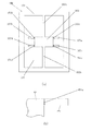
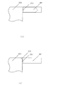
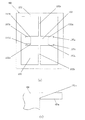
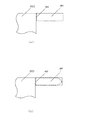
| US8324113B2 (en) | Silicon processing method and silicon substrate with etching mask | |
| JP5147366B2 (ja) | 異方性エッチングによる構造体の作製方法、及びエッチングマスク付きシリコン基板 | |
| JP2009031642A (ja) | 揺動体装置、光偏向器およびそれを用いた画像形成装置 | |
| JP5171489B2 (ja) | 異方性エッチングによる構造体の作製方法、及びエッチングマスク付きシリコン基板 | |
| JP7105934B2 (ja) | Memsミラー装置及びその製造方法 | |
| JP5353761B2 (ja) | 光偏向器の製造方法 | |
| JP2005279863A (ja) | アクチュエータの製造方法およびアクチュエータ | |
| JP2003315724A (ja) | 振動ミラーとその製造方法、光走査装置、画像形成装置 | |
| JP5624638B2 (ja) | シリコンの加工方法、及びエッチングマスク付きシリコン基板 | |
| JP2004198798A (ja) | 揺動体 | |
| JP2004347769A (ja) | 振動ミラー、光書込装置及び画像形成装置 | |
| JP6379763B2 (ja) | 光偏向器、光走査装置、画像形成装置及び画像投影装置 | |
| JP2015001543A (ja) | 光スキャナー、画像表示装置およびヘッドマウントディスプレイ | |
| JP2006309098A (ja) | リブと先細櫛歯を備えたmems走査ミラーの寸法諸元 | |
| CN109946831B (zh) | 促动器和其制造方法以及光扫描装置和其制造方法 |
Legal Events
| Date | Code | Title | Description |
|---|---|---|---|
| A521 | Request for written amendment filed |
Free format text: JAPANESE INTERMEDIATE CODE: A523 Effective date: 20101217 |
|
| A621 | Written request for application examination |
Free format text: JAPANESE INTERMEDIATE CODE: A621 Effective date: 20101217 |
|
| A761 | Written withdrawal of application |
Free format text: JAPANESE INTERMEDIATE CODE: A761 Effective date: 20110624 |