JP2009148847A - Manufacturing method for structure by anisotropic etching and silicon substrate with etching mask - Google Patents
Manufacturing method for structure by anisotropic etching and silicon substrate with etching mask Download PDFInfo
- Publication number
- JP2009148847A JP2009148847A JP2007327510A JP2007327510A JP2009148847A JP 2009148847 A JP2009148847 A JP 2009148847A JP 2007327510 A JP2007327510 A JP 2007327510A JP 2007327510 A JP2007327510 A JP 2007327510A JP 2009148847 A JP2009148847 A JP 2009148847A
- Authority
- JP
- Japan
- Prior art keywords
- etching mask
- etching
- correction
- silicon substrate
- mask
- Prior art date
- Legal status (The legal status is an assumption and is not a legal conclusion. Google has not performed a legal analysis and makes no representation as to the accuracy of the status listed.)
- Withdrawn
Links
- 238000005530 etching Methods 0.000 title claims abstract description 385
- 239000000758 substrate Substances 0.000 title claims abstract description 80
- XUIMIQQOPSSXEZ-UHFFFAOYSA-N Silicon Chemical compound [Si] XUIMIQQOPSSXEZ-UHFFFAOYSA-N 0.000 title claims abstract description 74
- 229910052710 silicon Inorganic materials 0.000 title claims abstract description 73
- 239000010703 silicon Substances 0.000 title claims abstract description 73
- 238000004519 manufacturing process Methods 0.000 title claims abstract description 36
- 229910021421 monocrystalline silicon Inorganic materials 0.000 claims abstract description 33
- 238000000034 method Methods 0.000 claims description 74
- 230000003287 optical effect Effects 0.000 claims description 49
- 238000005520 cutting process Methods 0.000 claims description 16
- XLYOFNOQVPJJNP-UHFFFAOYSA-N water Substances O XLYOFNOQVPJJNP-UHFFFAOYSA-N 0.000 claims description 6
- 230000015572 biosynthetic process Effects 0.000 claims description 5
- 238000005406 washing Methods 0.000 claims description 4
- 238000001035 drying Methods 0.000 claims description 2
- 239000000463 material Substances 0.000 description 22
- 239000000243 solution Substances 0.000 description 20
- 238000000347 anisotropic wet etching Methods 0.000 description 11
- KWYUFKZDYYNOTN-UHFFFAOYSA-M Potassium hydroxide Chemical compound [OH-].[K+] KWYUFKZDYYNOTN-UHFFFAOYSA-M 0.000 description 10
- 229910052581 Si3N4 Inorganic materials 0.000 description 9
- 230000002950 deficient Effects 0.000 description 9
- HQVNEWCFYHHQES-UHFFFAOYSA-N silicon nitride Chemical compound N12[Si]34N5[Si]62N3[Si]51N64 HQVNEWCFYHHQES-UHFFFAOYSA-N 0.000 description 9
- 239000013078 crystal Substances 0.000 description 7
- HEMHJVSKTPXQMS-UHFFFAOYSA-M Sodium hydroxide Chemical compound [OH-].[Na+] HEMHJVSKTPXQMS-UHFFFAOYSA-M 0.000 description 6
- 230000000694 effects Effects 0.000 description 5
- 238000000926 separation method Methods 0.000 description 5
- 238000001312 dry etching Methods 0.000 description 4
- 238000000206 photolithography Methods 0.000 description 4
- WGTYBPLFGIVFAS-UHFFFAOYSA-M tetramethylammonium hydroxide Chemical compound [OH-].C[N+](C)(C)C WGTYBPLFGIVFAS-UHFFFAOYSA-M 0.000 description 4
- XAGFODPZIPBFFR-UHFFFAOYSA-N aluminium Chemical compound [Al] XAGFODPZIPBFFR-UHFFFAOYSA-N 0.000 description 3
- 229910052782 aluminium Inorganic materials 0.000 description 3
- 238000010586 diagram Methods 0.000 description 3
- 238000004518 low pressure chemical vapour deposition Methods 0.000 description 3
- 238000012986 modification Methods 0.000 description 3
- 230000004048 modification Effects 0.000 description 3
- OAKJQQAXSVQMHS-UHFFFAOYSA-N Hydrazine Chemical compound NN OAKJQQAXSVQMHS-UHFFFAOYSA-N 0.000 description 2
- VYPSYNLAJGMNEJ-UHFFFAOYSA-N Silicium dioxide Chemical compound O=[Si]=O VYPSYNLAJGMNEJ-UHFFFAOYSA-N 0.000 description 2
- 238000000151 deposition Methods 0.000 description 2
- 239000004065 semiconductor Substances 0.000 description 2
- RYGMFSIKBFXOCR-UHFFFAOYSA-N Copper Chemical compound [Cu] RYGMFSIKBFXOCR-UHFFFAOYSA-N 0.000 description 1
- 230000001133 acceleration Effects 0.000 description 1
- 239000007864 aqueous solution Substances 0.000 description 1
- ONRPGGOGHKMHDT-UHFFFAOYSA-N benzene-1,2-diol;ethane-1,2-diamine Chemical compound NCCN.OC1=CC=CC=C1O ONRPGGOGHKMHDT-UHFFFAOYSA-N 0.000 description 1
- 229910052802 copper Inorganic materials 0.000 description 1
- 239000010949 copper Substances 0.000 description 1
- PCHJSUWPFVWCPO-UHFFFAOYSA-N gold Chemical compound [Au] PCHJSUWPFVWCPO-UHFFFAOYSA-N 0.000 description 1
- 229910052737 gold Inorganic materials 0.000 description 1
- 239000010931 gold Substances 0.000 description 1
- 238000000059 patterning Methods 0.000 description 1
- 230000035515 penetration Effects 0.000 description 1
- 108091008695 photoreceptors Proteins 0.000 description 1
- 230000001681 protective effect Effects 0.000 description 1
- 229910052814 silicon oxide Inorganic materials 0.000 description 1
- 238000001771 vacuum deposition Methods 0.000 description 1
Images


Classifications
-
- B—PERFORMING OPERATIONS; TRANSPORTING
- B81—MICROSTRUCTURAL TECHNOLOGY
- B81C—PROCESSES OR APPARATUS SPECIALLY ADAPTED FOR THE MANUFACTURE OR TREATMENT OF MICROSTRUCTURAL DEVICES OR SYSTEMS
- B81C1/00—Manufacture or treatment of devices or systems in or on a substrate
- B81C1/00388—Etch mask forming
- B81C1/00404—Mask characterised by its size, orientation or shape
Landscapes
- Engineering & Computer Science (AREA)
- Manufacturing & Machinery (AREA)
- Microelectronics & Electronic Packaging (AREA)
- Micromachines (AREA)
- Mechanical Light Control Or Optical Switches (AREA)
- Mechanical Optical Scanning Systems (AREA)
Abstract
Description
本発明は、異方性エッチングによる構造体の作製方法、エッチングマスク付きシリコン基板などに関する。より詳細には、エッチングマスク付き単結晶シリコン基板、これを用いた光偏向器などのマイクロ構造体等の構造体の作製方法、この作製方法により作製される光偏向器等に関する。この光偏向器は、例えば、光の偏向走査によって画像を投影するプロジェクションディスプレイや、電子写真プロセスを有するレーザビームプリンタ、デジタル複写機等の画像形成装置に好適に利用されるものである。 The present invention relates to a method for manufacturing a structure by anisotropic etching, a silicon substrate with an etching mask, and the like. More specifically, the present invention relates to a single crystal silicon substrate with an etching mask, a manufacturing method of a structure such as a micro structure using the same, an optical deflector manufactured by the manufacturing method, and the like. This optical deflector is suitably used for an image forming apparatus such as a projection display that projects an image by light deflection scanning, a laser beam printer having an electrophotographic process, a digital copying machine, and the like.
従来、半導体プロセスによってシリコン基板から製造される微小機械部材は、マイクロメータオーダの加工が可能であり、これらを用いて様々な微小機能素子が実現されている。特に、この様な技術によって形成される光偏向器は、ポリゴンミラー等の回転多面鏡を使用した光走査光学系に比べ、次の様な特徴がある。すなわち、光偏向器を小型化することが可能であること、消費電力が少ないこと、等の特徴がある。 Conventionally, micromechanical members manufactured from a silicon substrate by a semiconductor process can be processed on the order of micrometers, and various micro functional elements are realized using these. In particular, an optical deflector formed by such a technique has the following characteristics compared to an optical scanning optical system using a rotating polygonal mirror such as a polygon mirror. That is, the optical deflector can be miniaturized and has low power consumption.
この種の提案例として、半導体プロセスの一つである異方性ウェットエッチング技術を用いて作製した光偏向器がある(特許文献1参照)。また、異方性ウェットエッチング技術によってシリコン基板をエッチングして、所望の目標形状(基本エッチングマスクに対応する形状)にするための技術として、補正エッチングマスクを用いる提案例がある(特許文献2参照)。
しかしながら、シリコンの異方性ウェットエッチングにより目標形状を作製する場合、エッチング中やエッチング後に、基本エッチングマスクに繋がる補正エッチングマスクが剥がれたり、破壊されたりすることがある。そして、壊れた補正エッチングマスクが、形成されつつある目標形状に好ましくない態様で付着すると、最終形状の或る部分が所望の目標形状と異なる形状になる可能性がある。その或る部分が、形状的に多少異なっても機能に然程影響が現れない部分であればよいが、形状的に正確さが要求される部分である場合は、作製品の歩留まりが低下することになり得る。 However, when the target shape is produced by anisotropic wet etching of silicon, the correction etching mask that leads to the basic etching mask may be peeled off or destroyed during or after the etching. Then, if the broken correction etching mask adheres to the target shape being formed in an unfavorable manner, a portion of the final shape may be different from the desired target shape. The part may be a part that does not affect the function so much even if it is slightly different in shape, but if it is a part that requires accuracy in shape, the yield of the product is reduced. It can happen.
上記課題に鑑み、本発明の異方性エッチングによる構造体の作製方法は、マスク形成工程と目標形状形成工程とを有する。マスク形成工程では、単結晶シリコン基板上に、目標形状に対応する基本エッチングマスク、及び該基本エッチングマスクに接続する連結部を持つ補正エッチングマスクを形成する。マスク形成工程では、更に、局所的に機械的強度を低下させた強度低下部を上記補正エッチングマスクの連結部の少なくとも一部に形成する。目標形状形成工程では、異方性エッチングにより、上記シリコン基板をエッチングして目標形状を形成する。 In view of the above problems, the method for manufacturing a structure by anisotropic etching according to the present invention includes a mask formation step and a target shape formation step. In the mask forming step, a basic etching mask corresponding to the target shape and a correction etching mask having a connecting portion connected to the basic etching mask are formed on the single crystal silicon substrate. In the mask forming step, a strength reduction portion where the mechanical strength is locally reduced is further formed on at least a part of the connecting portion of the correction etching mask. In the target shape forming step, the silicon substrate is etched by anisotropic etching to form a target shape.
また、上記課題に鑑み、本発明のエッチングマスク付きシリコン基板は、単結晶シリコン基板上に、目標形状に対応する基本エッチングマスク、及び該基本エッチングマスクに接続する連結部を持つ補正エッチングマスクを有する。更に、局所的に機械的強度を低下させた強度低下部が、上記補正エッチングマスクの連結部の少なくとも一部に形成されている。 In view of the above problems, a silicon substrate with an etching mask of the present invention has a basic etching mask corresponding to a target shape and a correction etching mask having a connecting portion connected to the basic etching mask on a single crystal silicon substrate. . Further, a strength reduction portion where the mechanical strength is locally reduced is formed in at least a part of the connecting portion of the correction etching mask.
また、上記課題に鑑み、本発明の揺動体装置は次の特徴を有する。即ち、揺動体装置は、支持体と、支持体に対して可動に支持された可動部と、支持体に対して可動部を揺動軸回りに揺動可能に弾性的に連結する弾性支持部と、可動部を駆動する駆動手段とを有し、上記の構造体の作製方法により作製されることを特徴とする。 In view of the above problems, the oscillator device of the present invention has the following characteristics. That is, the oscillator device includes a support, a movable portion that is movably supported with respect to the support, and an elastic support portion that elastically couples the movable portion with respect to the support so as to be swingable about a swing axis. And a driving means for driving the movable portion, and is manufactured by the above-described manufacturing method of the structure.
また、上記課題に鑑み、本発明の光偏向器は、上記揺動体装置と、上記可動部に設けられた光偏向素子とを有することを特徴とする。 In view of the above problems, an optical deflector according to the present invention includes the oscillator device and an optical deflection element provided in the movable portion.
また、上記課題に鑑み、本発明の画像形成装置などの光学機器は、上記光偏向器を有し、該光偏向器が、光源からの光ビームを偏向し、該光ビームの少なくとも一部を感光体などの光照射対象物に入射させることを特徴とする。 Further, in view of the above problems, an optical apparatus such as the image forming apparatus of the present invention includes the optical deflector, and the optical deflector deflects a light beam from a light source, and at least part of the light beam is used. It is made to enter into light irradiation objects, such as a photoreceptor.
本発明によれば、上記の如き強度低下部を持つ補正エッチングマスクを用いるので、不都合な形で、基本エッチングマスクに繋がる補正エッチングマスクが剥がれたり、破壊されたりする可能性が少なくなる。よって、エッチングで形成される構造体の最終形状が所望の目標形状と異なる形状になる可能性を低減でき、構造体の不良品率を低減することができる。 According to the present invention, since the correction etching mask having the reduced strength portion as described above is used, the possibility that the correction etching mask connected to the basic etching mask is peeled off or destroyed in an inconvenient manner is reduced. Therefore, the possibility that the final shape of the structure formed by etching is different from a desired target shape can be reduced, and the defective product rate of the structure can be reduced.
以下に、本発明の実施の形態について図を用いて説明する。
本発明の異方性エッチングによる構造体の作製方法や本発明のエッチングマスクが形成された単結晶シリコン基板においては、基本的に、次の要件が満たされる必要がある。まず、単結晶シリコン基板上に、目標形状に対応する基本エッチングマスク、及び該基本エッチングマスクに接続する連結部を持つ補正エッチングマスクを形成する(マスク形成工程)。上記補正エッチングマスクは、その連結部の少なくとも一部に、局所的に機械的強度を低下させた強度低下部が形成されている。そして、上記基本エッチングマスクと上記補正エッチングマスクとを有する単結晶シリコン基板を異方性エッチングし上記目標形状を形成する(目標形状形成工程)。この際、上記補正エッチングマスクを形成した部分の単結晶シリコン基板はエッチングにより除去される。
Hereinafter, embodiments of the present invention will be described with reference to the drawings.
In the method for manufacturing a structure by anisotropic etching according to the present invention and the single crystal silicon substrate on which the etching mask according to the present invention is formed, the following requirements must be basically satisfied. First, a correction etching mask having a basic etching mask corresponding to a target shape and a connecting portion connected to the basic etching mask is formed on a single crystal silicon substrate (mask forming process). In the correction etching mask, a strength reduction portion in which the mechanical strength is locally reduced is formed in at least a part of the connecting portion. Then, the single crystal silicon substrate having the basic etching mask and the correction etching mask is anisotropically etched to form the target shape (target shape forming step). At this time, the portion of the single crystal silicon substrate on which the correction etching mask is formed is removed by etching.
典型的には、上記強度低下部は、基本エッチングマスクの所定の重要な部分に接続する補正エッチングマスクの連結部に形成される。所定の重要な部分とは、例えば、後述する可動部の様に形状的に正確さが要求される部分に対応する基本エッチングマスクの部分である。後述する実施形態や実施例では、構造体として、可動部と支持体と弾性支持部を有するものを示すが、本発明において、構造体はこれに限定されるものではない。つまり、凸部コーナを有する可動部の如き部分を含む揺動体装置の様な構造体が典型例であるが、どのような構造体にも適用することができる。例えば、マイクロマシン技術を用いて作製する加速度センサや角速度センサ等のマイクロ構造体などの構造体にも適用することができる。 Typically, the strength reduction portion is formed at a connection portion of the correction etching mask connected to a predetermined important portion of the basic etching mask. The predetermined important part is, for example, a part of the basic etching mask corresponding to a part that requires accuracy in shape like a movable part described later. In the embodiments and examples to be described later, a structure having a movable part, a support, and an elastic support is shown, but the structure is not limited to this in the present invention. That is, a structure such as an oscillator device including a movable part having a convex corner is a typical example, but the structure can be applied to any structure. For example, the present invention can be applied to a structure such as a micro structure such as an acceleration sensor or an angular velocity sensor manufactured using a micromachine technique.
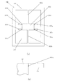
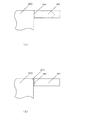
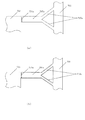
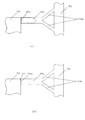
図1(a)は、本発明の一実施形態のマイクロ構造体などの構造体のエッチングマスクを示す上面図であり、図1(b)は補正エッチングマスクの一部の拡大図である。また、図2−1は、異方性エッチングによって単結晶シリコン基板をエッチングして作製するマイクロ構造体などの構造体を示す上面図であり、図2−2はその断面図である。また、図3−1と図3−2は、本実施形態の補正エッチングマスクの一部の拡大上面図であり、補正エッチングマスクの下の単結晶シリコン基板が異方性エッチングによってどの様にエッチングされるかを説明するための図である。 FIG. 1A is a top view showing an etching mask of a structure such as a microstructure according to an embodiment of the present invention, and FIG. 1B is an enlarged view of a part of the correction etching mask. FIG. 2-1 is a top view showing a structure such as a microstructure manufactured by etching a single crystal silicon substrate by anisotropic etching, and FIG. 2-2 is a cross-sectional view thereof. FIGS. 3A and 3B are enlarged top views of a part of the correction etching mask of the present embodiment, and how the single crystal silicon substrate under the correction etching mask is etched by anisotropic etching. It is a figure for demonstrating what is done.
本実施形態の構造体の作製方法では、支持体201と、弾性支持部202a、202bと、揺動軸であるねじり軸207回りに揺動可能な可動部203とを有する図2−1に示す様な構造体が目標形状である。弾性支持部202a、202bは、支持体201に対して可動部203を揺動軸回りに揺動可能に弾性的に連結している。この構造体は、反射面204を有し、図2−2に示す様な磁性体205及びコイル206を有しているので、反射面204で入射光を反射・偏向する光偏向器として利用することができる。
The structure manufacturing method of this embodiment is shown in FIG. 2A having a
本実施形態の構造体の作製方法では、(100)面を主面とする単結晶シリコン基板を異方性ウェットエッチングすることによって、目標形状が形成される。異方性ウェットエッチングとは、特定の結晶方位に対してエッチングが進まない性質を有するエッチング液を用いるエッチングであり、特定の結晶面を基準とした構造、即ちこうした結晶面で画された構造体を非常に高い加工精度で作製することができる。異方性エッチング液には、KOH(水酸化カリウム)、TMAH(水酸化テトラメチルアンモニウム水溶液)、EDP(エチレンジアミンピロカテコール+水)、NaOH(水酸化ナトリウム)、ヒドラジン等がある。 In the structure manufacturing method of this embodiment, a target shape is formed by performing anisotropic wet etching on a single crystal silicon substrate having a (100) plane as a main surface. Anisotropic wet etching is an etching that uses an etchant having a property that etching does not proceed with respect to a specific crystal orientation, and has a structure based on a specific crystal plane, that is, a structure defined by such a crystal plane. Can be manufactured with very high processing accuracy. Examples of the anisotropic etching solution include KOH (potassium hydroxide), TMAH (tetramethylammonium hydroxide aqueous solution), EDP (ethylenediamine pyrocatechol + water), NaOH (sodium hydroxide), hydrazine, and the like.
異方性エッチング溶液により単結晶シリコン基板をエッチングする場合、シリコン基板を目標形状に忠実にエッチングするために、目標形状である基本エッチングマスクと共に、目標形状の凸部を保護するための補正エッチングマスクが用いられる。つまり、補正エッチングマスクは、シリコン基板を目標形状に加工するまでエッチングしている間、目標形状の凸部がエッチングされてしまうのを防止する。図1の基本エッチングマスクは、支持体201、弾性支持部202a、202b、可動部203に夫々対応する部分101、102a、102b、103(以下において、こうしたマスク部分を支持体101などと記すこともある)を含む。また、補正エッチングマスクは、部分107a、107b、107c、107d(以下において、部分107aなどを補正エッチングマスク107aなどと記すこともある)を含む。こうして、図2−1に示す支持体201、弾性支持部202a、202b、可動部203が作製されるまで、図1の補正エッチングマスク107a、107b、107c、107dが可動部203の凸部コーナがエッチングされるのを防止する。
When etching a single crystal silicon substrate with anisotropic etching solution, in order to etch the silicon substrate faithfully to the target shape, along with the basic etching mask that is the target shape, a correction etching mask to protect the convex part of the target shape Is used. In other words, the correction etching mask prevents the convex portion of the target shape from being etched while etching until the silicon substrate is processed into the target shape. The basic etching mask of FIG. 1 has
本実施形態の構造体の作製方法を説明する。まず、単結晶シリコン基板100の両面に、マスク材料を成膜する。マスク材料は、シリコン基板が異方性エッチング溶液でエッチングされている間、消失しない材料であればよい。例えば、窒化シリコン膜や酸化シリコン膜等である。マスク材料をフォトリソグラフィ及びパターニングすることによって、図1に示す様なマスクパターンを形成することができる。マスクパターン形成後、シリコン基板100を異方性エッチング溶液に浸すことによってシリコン貫通部120が形成され、図2−1に示す様な最終形状を形成することができる。
A method for manufacturing the structure according to this embodiment will be described. First, a mask material is formed on both surfaces of the single
この際、シリコン基板100の側面がエッチング溶液に晒される場合には、側面にもマスク材料を成膜しておく。なお、マスクパターンは単結晶シリコン基板100の片面だけに形成し、その他の面はマスク材料を成膜しておいて、エッチングを実行することもできる。ただし、この場合は、エッチングのされ方が後述する図10に示すものとは異なる。また、一枚のシリコン基板上に、構造体を複数並べて作製することができる。その場合、各構造体は隣接しているので、シリコン基板の側面にマスク材料を成膜しておけばよい。
At this time, if the side surface of the
本実施形態の構造体の作製方法では、補正エッチングマスク107a、107b、107c、107dは、基本エッチングマスクである可動部103と連結している。補正エッチングマスク各々の可動部103との連結部には、1つ以上の貫通孔151a、152b、153c、154dがある。すなわち、基本エッチングマスクの所定の部分に接続する補正エッチングマスクの連結部に、局所的に機械的強度を低下させた強度低下部が形成されている。
In the structure manufacturing method of this embodiment, the
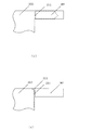
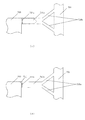
本実施形態の構造体の作製方法における補正エッチングマスクの作用・効果を説明する。図3−1と図3−2は、図1の補正エッチングマスクの部分107aにおけるエッチング過程を拡大して示し、図1の対応する部分を3百番台の数字で示す図である。図3−1(a)に示す様に、単結晶シリコン基板上に可動部の基本エッチングマスク303が形成される。更に、補正エッチングマスク307が形成され、可動部の基本エッチングマスク303の凸部コーナと連結している。補正エッチングマスク307の連結部には、強度低下部を構成する複数の貫通孔351が形成さている。
The operation and effect of the correction etching mask in the structure manufacturing method of this embodiment will be described. FIGS. 3A and 3B are enlarged views of the etching process in the correction
図3−1(b)の破線で示す様に、シリコン基板を異方性ウェットエッチング溶液に浸すと、エッチングが進み、補正エッチングマスク307の端の凸部において、マスク下のシリコンがエッチングされていく。更にエッチングが進むと、図3−2(c)の破線で示す様に、シリコン基板はエッチングされてしまい、補正エッチングマスク307下のシリコン部分がエッチングされる。最終的に、図3−2(d)に示す様に、可動部の基本エッチングマスク303下のシリコン部分が残り、最終形状となる。最終形状では、補正エッチングマスク下のシリコンをすべてエッチングする間に、サイドエッチングが進み、凸部が僅かにエッチングされて図3−2(d)の破線で示すサイドエッチング部311が形成される。補正エッチングマスクは、基本エッチングマスクに連結されているので、最終形状が作製されて補正エッチングマスクの下にシリコンがなくなっても、補正エッチングマスクの片端は基本エッチングマスクと連結している。
As shown by the broken line in FIG. 3B, when the silicon substrate is immersed in an anisotropic wet etching solution, the etching proceeds, and the silicon under the mask is etched at the convex portion at the end of the
このとき、補正エッチングマスク307において、貫通孔351の下のシリコンもなくなっている。そのため、補正エッチングマスク307の貫通孔351の箇所は、ミシン目状の形状となり、強度低下部となっている。
At this time, silicon under the through
強度低下部は、補正エッチングマスクのマスク材料の貫通孔の形態だけに限らない。図4や図5−1と図5−2に示す様な補正エッチングマスクのマスクの切れ込み152、552の形態や、図6や図7−1と図7−2に示す様な補正エッチングマスクのマスク材料の薄肉部153、653の形態であっても構わない。或いは、それらの組み合わせ等であっても構わない。
The strength reduction portion is not limited to the form of the through hole of the mask material of the correction etching mask. As shown in FIG. 4, FIG. 5-1, and FIG. 5-2, the
図4及び図5−1と図5−2は、1つ以上の切れ込み152、552で強度低下部を構成した変形形態を示す。図5−1と図5−2は、図4の補正エッチングマスクの部分におけるエッチング過程を拡大して示し、図4の対応する部分を5百番台の数字で示す図である。シリコン基板100を異方性ウェットエッチング溶液に浸すと、図5−1と図5−2の破線で示す様に、エッチングが進み、最終形状となる。ここでも、最終形状では、補正エッチングマスク下のシリコンをすべてエッチングする間に、サイドエッチングが進み、凸部が僅かにエッチングされて図5−2(d)の破線で示すサイドエッチング部511が形成される。
4 and 5-1 and FIG. 5-2 show a modification in which the strength reduction portion is configured by one or
図6及び図7−1と図7−2は、1つ以上の薄肉部153、653で強度低下部を構成した変形形態を示す。図7−1と図7−2は、図6の補正エッチングマスクの部分におけるエッチング過程を拡大して示し、図6の対応する部分を6百番台の数字で示す図である。シリコン基板100を異方性ウェットエッチング溶液に浸すと、図6−1と図6−2の破線で示す様に、エッチングが進み、最終形状となる。ここでも、最終形状では、補正エッチングマスク下のシリコンをすべてエッチングする間に、サイドエッチングが進み、凸部が僅かにエッチングされて図7−2(d)の破線で示すサイドエッチング部611が形成される。
6 and FIGS. 7-1 and FIG. 7-2 show a modification in which the strength-decreasing portion is constituted by one or more thin-
次に、本実施形態の補正エッチングマスクのマスク材料を、強度低下部の形成された連結部で切断する工程を説明する。補正エッチングマスクは最終的には除去される必要があるので、こうした工程を行う必要がある。勿論、エッチング工程の最終段階において、既に補正エッチングマスクが強度低下部のところで分離されてしまっていれば、こうした切断工程は不要となる。基本エッチングマスクについては、支障が無ければそのまま残しておいてもよいし、除去が必要なら、別途のエッチング工程で除去すればよい。補正エッチングマスクも、基本エッチングマスクの除去工程で一緒に除去してもよい。後述する図8に示す様な形態の補正エッチングマスクの場合は、基本エッチングマスクと一緒に別途のエッチング工程で除去する方がよい場合もある。 Next, a process of cutting the mask material of the correction etching mask of the present embodiment at the connecting portion where the strength reduction portion is formed will be described. Since the correction etching mask needs to be finally removed, it is necessary to perform such a process. Of course, if the correction etching mask has already been separated at the reduced strength portion in the final stage of the etching process, such a cutting process becomes unnecessary. The basic etching mask may be left as it is if there is no problem, or may be removed in a separate etching step if it is necessary to remove it. The correction etching mask may also be removed together in the basic etching mask removal process. In the case of a correction etching mask having a form as shown in FIG. 8 described later, it may be better to remove the correction etching mask together with the basic etching mask in a separate etching process.
上記補正エッチングマスクの切断の1つ目の方法は、異方性エッチングのための異方性エッチング溶液中において単結晶シリコン基板に揺動運動を与えることにより、応力が弱い強度低下部の形成された連結部で切断する方法である。
2つ目の方法は、異方性エッチングのための異方性エッチング溶液中において単結晶シリコン基板に回転運動を与えることにより、応力が弱い強度低下部の形成された連結部で切断する方法である。
3つ目の方法は、シリコン基板の水洗中において単結晶シリコン基板にウォータシャワを当てることにより、応力が弱い強度低下部の形成された連結部で切断する方法である。
4つ目の方法は、シリコン基板の乾燥中において単結晶シリコン基板にエアを当てることにより、応力が弱い強度低下部の形成された連結部で切断する方法である。
5つ目の方法は、異方性エッチングのための異方性エッチング溶液中或いはシリコン基板の水洗中において、単結晶シリコン基板に超音波振動を当てることにより、応力が弱い強度低下部の形成された連結部で切断する方法である。
The first method of cutting the correction etching mask is to form a reduced strength portion where the stress is weak by applying a swinging motion to the single crystal silicon substrate in an anisotropic etching solution for anisotropic etching. It is the method of cut | disconnecting with the connected part.
The second method is a method in which a single crystal silicon substrate is subjected to rotational movement in an anisotropic etching solution for anisotropic etching, thereby cutting at a connecting portion where a strength reduction portion where stress is weak is formed. is there.
The third method is a method in which a water crystal is applied to a single crystal silicon substrate during water washing of the silicon substrate to cut at a connecting portion in which a reduced strength portion having a low stress is formed.
The fourth method is a method in which air is applied to the single crystal silicon substrate during the drying of the silicon substrate to cut at the connecting portion where the strength reduction portion where the stress is weak is formed.
The fifth method is to form a strength reduction part where the stress is weak by applying ultrasonic vibration to the single crystal silicon substrate in the anisotropic etching solution for anisotropic etching or in the water washing of the silicon substrate. It is the method of cut | disconnecting with the connected part.
次に、他の実施の形態を説明する。
他の実施の形態では、基本エッチングマスクと補正エッチングマスクを以下のように作製する。単結晶シリコン基板上に、凸部コーナを有する第1の構造体(可動部)と第1の構造体と開口部を介して隣接する第2の構造体(支持体)とを少なくとも有する目標形状(揺動体装置)に対応するマスクを基本エッチングマスクとする。また、第1の構造体のエッチングマスクの凸部コーナから伸びて第2の構造体のエッチングマスクと連結するマスクを補正エッチングマスクとする。本実施形態においても、マスク形成工程において、第1の構造体の基本エッチングマスクと補正エッチングマスクとが連結する連結部の少なくとも一部に、局所的に機械的強度を低下させた強度低下部を形成する。また、補正エッチングマスクは、第1の構造体のエッチングマスクの凸部コーナから[110]方向に伸びると共に、[100]方向に分岐したそれぞれの補正エッチングマスクが第2の構造体のエッチングマスクと連結するY字形状を有してもよい。
Next, another embodiment will be described.
In another embodiment, a basic etching mask and a correction etching mask are produced as follows. A target shape having at least a first structure (movable part) having a convex corner and a second structure (support) adjacent to the first structure through an opening on a single crystal silicon substrate A mask corresponding to (oscillator device) is a basic etching mask. A mask that extends from the convex corner of the etching mask of the first structure and is connected to the etching mask of the second structure is used as a correction etching mask. Also in the present embodiment, in the mask formation step, at least a part of the connecting portion where the basic etching mask and the correction etching mask of the first structure are connected has a strength-decreasing portion in which the mechanical strength is locally reduced Form. The correction etching mask extends in the [110] direction from the convex corner of the etching mask of the first structure, and each correction etching mask branched in the [100] direction is connected to the etching mask of the second structure. You may have a Y-shape to connect.
以下図面を用いて説明する。
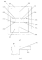
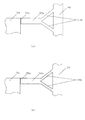
図8に示す補正エッチングマスク707a、707b、707c、707dは、基本エッチングマスク703の凸部コーナと連結しており、Siの結晶方位である[110]方向に伸びている。一方、補正エッチングマスクの他端710a、710b、710c、710dは、補正エッチングマスク707a、707b、707c、707dから[100]方向に分岐し、支持体701と連結する。補正エッチングマスク707a、707b、707c、707dは、可動部の基本エッチングマスク703の凸部コーナと連結し、且つ、一方向に伸びている長方形である。そして、補正エッチングマスク707a、707b、707c、707dは、これらとは別の方向に伸びている長方形である補正エッチングマスク710a、710b、710c、710dと連結している。補正エッチングマスク710a、710b、710c、710dは、全て支持体の基本エッチングマスク701と連結する。更に、補正エッチングマスク707a、707b、707c、707d各々の可動部703との連結部には、少なくも1つの貫通孔751a、752b、753c、754dがある。
This will be described below with reference to the drawings.
The
図9−1及び図9−2は、図8の補正エッチングマスクの一部の拡大図である。本実施形態でも、図8に示す様に、単結晶シリコン基板700上に、可動部の基本エッチングマスク703と支持体の基本エッチングマスク701と弾性支持部の基本エッチングマスク702a、702bが形成される。更に、補正エッチングマスクが形成され、可動部の基本エッチングマスク703と支持体の基本エッチングマスク701と連結している。
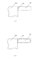
FIGS. 9A and 9B are enlarged views of a part of the correction etching mask of FIG. Also in this embodiment, as shown in FIG. 8, the
図9−1(b)に示す様に、シリコン基板700を異方性ウェットエッチング溶液に浸すと、エッチングが進むとともに、主に、補正エッチングマスク710a下のシリコンもエッチングされていく。更にエッチングが進むと、図9−2(c)に示す様に、補正エッチングマスク710a下のシリコン基板はエッチングされてしまい、補正エッチングマスク707a下のシリコン部分がエッチングされる。最終的に、図9−2(d)に示す様に、シリコン貫通部720が形成されて可動部の基本エッチングマスク703下のシリコン部分が残り、最終形状となる。最終形状では、補正エッチングマスク下のシリコンをすべてエッチングする間に、サイドエッチングが進み、凸部が僅かにエッチングされて図9−2(d)の破線で示すサイドエッチング部711が形成される。補正エッチングマスクは、基本エッチングマスクに連結されているので、最終形状が作製され補正エッチングマスクの下にシリコンがなくなっても、補正エッチングマスクの両端は基本エッチングマスクと連結している。
As shown in FIG. 9-1 (b), when the
このとき、補正エッチングマスク707aにおいて、貫通孔751aの下のシリコンもなくなっている。そのため、補正エッチングマスク707aの貫通孔751aの箇所は、ミシン目状の形状となり、強度低下部となっている。ここで、強度低下部は、可動部のみと連結されている上記図1の実施形態の補正エッチングマスクと同様である。すなわち、補正エッチングマスクのマスク材料の貫通孔だけでなく、補正エッチングマスクのマスクの切れ込みや、補正エッチングマスクのマスク材料の薄肉部、或いはそれらの組み合わせであっても構わない。
At this time, silicon under the through
図11及び図12−1と図12−2は、少なくも1つの切れ込み752で強度低下部を構成した変形形態を示す。図12−1と図12−2は、図11の補正エッチングマスクの部分におけるエッチング過程を拡大して示す。シリコン基板700を異方性ウェットエッチング溶液に浸すと、図12−1と図12−2の破線で示す様に、エッチングが進み、最終形状となる。ここでも、最終形状では、補正エッチングマスク下のシリコンをすべてエッチングする間に、サイドエッチングが進み、凸部が僅かにエッチングされて図12−2(d)の破線で示すサイドエッチング部711が形成される。
FIGS. 11 and 12-1 and FIG. 12-2 show a modification in which the strength-decreasing portion is configured by at least one notch 752. FIG. FIGS. 12A and 12B are enlarged views of the etching process in the correction etching mask portion of FIG. When the
図13及び図14−1と図14−2は、少なくも1つの薄肉部753で強度低下部を構成した変形形態を示す。図14−1と図14−2は、図13の補正エッチングマスクの部分におけるエッチング過程を拡大して示す。シリコン基板700を異方性ウェットエッチング溶液に浸すと、図14−1と図14−2の破線で示す様に、エッチングが進み、最終形状となる。ここでも、最終形状では、補正エッチングマスク下のシリコンをすべてエッチングする間に、サイドエッチングが進み、凸部が僅かにエッチングされて図14−2(d)の破線で示すサイドエッチング部711が形成される。
13 and 14-1 and FIG. 14-2 show a modified form in which the strength-decreasing portion is constituted by at least one thin-walled portion 753. FIG. FIGS. 14A and 14B are enlarged views of the etching process in the correction etching mask portion of FIG. When the
本実施形態でも、強度低下部の形成された連結部での切断方法については、可動部のみと連結されている補正エッチングマスクとほぼ同様である。ただし、本実施形態では、強度低下部の無い連結部がある。このことの影響について説明する。 Also in this embodiment, the cutting method at the connecting portion where the strength reduction portion is formed is almost the same as that of the correction etching mask connected to only the movable portion. However, in this embodiment, there exists a connection part without an intensity | strength reduction part. The effect of this will be described.
図10は、図8のA1−A2断面図である。ここでは、シリコン基板700の両面にマスクパターンが形成されている。図10(a)は、エッチングマスクが形成されたシリコン基板の断面図であり、図10(b)は、エッチングが終了した時のシリコン基板700の断面図である。図10(b)に示す様に、エッチング終了時の補正エッチングマスク707a、707b、707e、707f、710a、710b、710e、710f下のシリコンがエッチングされている。こうして、強度低下部751a、751b、751e、751fを持つ補正エッチングマスクが片支持状に近い状態になっている。従って、補正エッチングマスクは強度低下部で非常に壊れやすい。また、補正エッチングマスクは、その下のシリコンがエッチングされてシリコン基板がないと共に、補正エッチングマスクの厚みは、サブミクロンオーダーであり非常に薄いため、非常に壊れやすくなっている。また、成膜時にマスク材料には残留応力があるために、シリコン基板がエッチングされた後は、応力によって、補正エッチングマスクが変形しやすい。なお、図10において、701a、701b、701e、701f、703a、703bは、シリコン基板700の上下面上の基本エッチングマスクを示す。
10 is a cross-sectional view taken along line A1-A2 of FIG. Here, mask patterns are formed on both surfaces of the
図10(c)の様に、補正エッチングマスクがエッチング途中に壊れて、エッチングされるシリコン部分に付着した場合、付着したシリコンはエッチングされなくなる。また、他のエッチングマスク上に付着した場合は、付着した部分のマスクの厚みは二倍になってしまう。従って、エッチングマスクを剥離する工程において、付着した部分にマスク材料が残ってしまったり、剥離工程時間を二倍にしたりする必要がある。剥離時間を長くした場合、シリコン部分も削れてしまうことがある。この様に、最終形状が目標形状と異なる形状になる可能性がある。 As shown in FIG. 10C, when the correction etching mask is broken during etching and adheres to the silicon portion to be etched, the adhered silicon is not etched. Moreover, when it adheres on another etching mask, the thickness of the mask of the adhering part will be doubled. Therefore, in the process of peeling the etching mask, it is necessary to leave the mask material on the attached portion or double the peeling process time. If the peeling time is increased, the silicon portion may be removed. In this way, the final shape may be different from the target shape.
本実施形態の構造体の作製方法では、補正エッチングマスクを用いるが、非常に壊れやすくなっている補正エッチングマスクのマスク材料に前もって強度低下部を作製しておく。これにより、異方性エッチング溶液によりエッチングして目標形状を形成する工程で、全ての補正エッチングマスクのマスク材料の強度低下部において、マスク切断や分離除去が起こりやすい。しかし、ここでは、強度低下部は、可動部の基本エッチングマスクとの連結部に形成されているので、こうしたマスク切断や分離除去が起こっても、補正エッチングマスクは目標形状の可動部には付着しづらくなる。従って、正確に目標形状に形成される必要のある可動部は、たとえマスク切断や分離除去が起こっても、補正エッチングマスクの付着による影響を受けない可能性が高くなる。図10(c)はこうした状況を示している。こうして、形状に正確さが要求される重要な部分が目標形状と異なる形状となる事態を回避する可能性が高くすることができて、不良品率を低減することができる。つまり、本実施形態では、たとえエッチング途中で補正エッチングマスクが壊れても、可動部への影響があまり出ない可能性を高める様に補正エッチングマスクに強度低下部を設けている。 In the structure manufacturing method of the present embodiment, a correction etching mask is used. However, a reduced-strength portion is prepared in advance in the mask material of the correction etching mask that is very fragile. As a result, in the step of forming a target shape by etching with an anisotropic etching solution, mask cutting and separation / removal are likely to occur in the reduced strength portions of the mask material of all correction etching masks. However, here, the reduced strength part is formed at the connecting part of the movable part to the basic etching mask, so that the correction etching mask adheres to the movable part of the target shape even if such mask cutting or separation removal occurs. It becomes difficult. Therefore, the movable portion that needs to be accurately formed in the target shape is highly likely not to be affected by the adhesion of the correction etching mask even if mask cutting or separation / removal occurs. FIG. 10 (c) shows such a situation. In this way, it is possible to increase the possibility of avoiding a situation where an important part requiring accuracy in the shape is different from the target shape, and the defective product rate can be reduced. In other words, in the present embodiment, even if the correction etching mask is broken during the etching, the correction etching mask is provided with the strength reduction portion so as to increase the possibility that the movable portion is hardly affected.
上記のことは、可動部のみと連結されている補正エッチングマスクであっても、可動部と支持体の両方と連結されている補正エッチングマスクであっても、ほぼ同様である。すなわち、可動部の基本エッチングマスクと連結する補正エッチングマスクの連結部に強度低下部を形成しておけば、両者とも上記の理由で不良品率を低減することができる。 The above is substantially the same regardless of whether the correction etching mask is connected to only the movable part or the correction etching mask connected to both the movable part and the support. That is, if the strength reduction portion is formed in the connecting portion of the correction etching mask that is connected to the basic etching mask of the movable portion, both can reduce the defective product rate for the above reasons.
上記実施形態は、基本エッチングマスク及び補正エッチングマスクを単結晶シリコン基板の両面に同形状で上下整列して形成する構造体の作製方法とすることもできる。この作製方法によって、両面に同じ形状の構造体を作製することができる。両面に補正エッチングマスクが存在し、補正エッチングマスクが壊れる可能性は多少増えるが、従来例よりは不良品率を低減することができる。 The above embodiment can also be a method for manufacturing a structure in which a basic etching mask and a correction etching mask are formed in the same shape and vertically aligned on both surfaces of a single crystal silicon substrate. By this manufacturing method, structures having the same shape on both surfaces can be manufactured. Although there is a correction etching mask on both sides and the possibility that the correction etching mask is broken is somewhat increased, the defective product rate can be reduced as compared with the conventional example.
また、上記実施形態の構造体の作製方法により、支持体と、可動部と、支持体に対して可動部を揺動軸回りに揺動可能に弾性的に連結する弾性支持部と、可動部を駆動させる駆動手段とを有する揺動体装置を作製することができる。図2−2に示す様な磁性体205及びコイル206が駆動手段を構成する。この作製方法により作製される揺動体装置の不良品率を低減することができるので、比較的安価な揺動体装置を提供することができる。
Further, according to the structure manufacturing method of the above-described embodiment, the support, the movable portion, the elastic support portion that elastically couples the movable portion to the support body so as to swing about the swing axis, and the movable portion. It is possible to manufacture an oscillator device having a driving means for driving the. A
また、上記揺動体の可動部装置上に光偏向素子を設けて光偏向器を作製することもできる。光偏向器では、図2−2に示す様な反射面204で入射光を反射・偏向する。ここでも、光偏向器の不良品率を低減できるので、安価な光偏向器を提供することができる。
Further, an optical deflector can be manufactured by providing an optical deflection element on the movable part device of the oscillator. In the optical deflector, incident light is reflected and deflected by a reflecting
更に、光源と、上記光偏向器と、感光体などの光照射対象物とを有し、光偏向器が光源からの光を偏向し、光の少なくとも一部を感光体などの光照射対象物上に入射させる画像形成装置などの光学機器を作製することもできる。ここでも、安価な光偏向器を用いているので、比較的安価な光学機器を提供することができる。 Furthermore, it has a light source, the light deflector, and a light irradiation object such as a photoconductor, the light deflector deflects light from the light source, and at least part of the light is a light irradiation object such as a photoconductor. An optical device such as an image forming apparatus that is incident on the top can also be manufactured. Again, since an inexpensive optical deflector is used, a relatively inexpensive optical device can be provided.
また、本発明の補正エッチングマスクを形成するために、異方性エッチングによるエッチング工程の前工程においてフォトリソグラフィ工程で使用する石英ガラスなどで作製する工具、すなわちフォトマスクも提供することができる。 In addition, in order to form the correction etching mask of the present invention, a tool made of quartz glass or the like used in the photolithography process in the pre-process of the etching process by anisotropic etching, that is, a photomask can be provided.
以下、図に沿って、本発明の具体的な実施例を説明する。
(実施例1)
実施例1の光偏向器の構成、駆動方法、作製方法を図1、図2−1、図2−2、図3−1、図3−2を用いて説明する。図1(a)は、本実施例の光偏向器のエッチングマスクの上面図であり、図1(b)は本実施例のエッチングマスクを説明するための図1(a)の補正エッチングマスクの拡大図である。また、図2−1、図2−2は、異方性エッチングによって単結晶シリコン基板をエッチングして作製される光偏向器を説明する図である。
Hereinafter, specific examples of the present invention will be described with reference to the drawings.
(Example 1)
A configuration, a driving method, and a manufacturing method of the optical deflector according to the first embodiment will be described with reference to FIGS. 1, 2-1, 2-2, 3-1, and 3-2. FIG. 1A is a top view of an etching mask of the optical deflector of this embodiment, and FIG. 1B is a diagram of the correction etching mask of FIG. 1A for explaining the etching mask of this embodiment. It is an enlarged view. FIGS. 2A and 2B are diagrams illustrating an optical deflector manufactured by etching a single crystal silicon substrate by anisotropic etching.
図2−1、図2−2に示す様に、本実施例の光偏向器は、支持体201と、可動部203と、弾性支持部202a、202bを有する。弾性支持部202a、202bは、可動部203を支持体201に対してねじり軸207回りに揺動可能に弾性的に連結している。可動部203上には、反射面204が形成されている。本実施例では、反射面204の材料はアルミニウムであり、真空蒸着により形成されている。しかし、反射面204は別の材質、例えば金、銅等でもよく、更に保護膜或いは誘電体多層膜を形成してもよい。例えば、可動部203は、ねじり軸207に垂直な方向の長さが1.3mm、ねじり軸207に平行な方向の長さが1.5mm、厚さが0.2mmである。光偏向器のチップ全長は、例えば、10mmである。
As shown in FIGS. 2-1 and 2-2, the optical deflector of the present embodiment includes a
本実施例の光偏向器の駆動原理について説明する。図2−2に示す様に、可動部203は、硬磁性体205を有しており、これはねじり軸に対して垂直方向に磁化されている。コイル206に印加する電流は交流であり、交流の周波数に応じた磁場が発生し、この磁場が可動部203の硬磁性体205に力を及ぼす。こうして、可動部203にトルクが印加され、ねじり振動で光偏向器を駆動することができる。更には、本実施例の光偏向器が有する共振周波数と同じ交流電流をコイル206に流すことによって、低消費電力でねじり振動させることができる。
The driving principle of the optical deflector of this embodiment will be described. As shown in FIG. 2-2, the
本実施例の作製方法を図1を用いて説明する。単結晶シリコン基板100の両面に、窒化シリコン膜をLPCVD(Low Pressure CVD)によって約2000Å成膜する。窒化シリコン膜は、水酸化カリウム溶液に対して高い耐性を有するため、シリコン基板100が異方性エッチング溶液でエッチングされている間、消失しない。次に、図1に示すエッチングマスクパターンになる様に、フォトリソグラフィによって単結晶シリコン基板100の両面をパターニングする。その後、110℃に加熱した異方性エッチング溶液である水酸化カリウム溶液(30%重量濃度、)によって、パターニングしたシリコン単結晶基板100をエッチングする。エッチング終了後、エッチングマスクである窒化シリコン膜をドライエッチングにより剥離する。最後に、反射面204となるアルミニウムを成膜することによって、図2−1に示す様な最終形状を形成することができる。
A manufacturing method of this example will be described with reference to FIGS. A silicon nitride film is formed on both surfaces of the single
本実施例の構造体の作製方法では、補正エッチングマスク107a、107b、107c、107dは、夫々、基本エッチングマスクである可動部103の凸部コーナと連結している。補正エッチングマスク各々の可動部103との連結部には、少なくも1つの貫通孔151a、152b、153c、154dがある。
In the structure manufacturing method of this embodiment, the
本実施例のエッチング過程は、上述の実施形態の説明で図3−1、図3−2を参照しつつ述べた通りである。上述した様に、補正エッチングマスクは、基本エッチングマスクに連結されているので、最終形状が作製されて補正エッチングマスクの下にシリコンがなくなっても、補正エッチングマスクの片端は基本エッチングマスクと連結している。このとき、補正エッチングマスク307において、貫通孔351の箇所はミシン目状の形状となり、強度低下部となっている。この補正エッチングマスクのマスク材料を強度低下部で切断して除去する方法としては、幾つかの方法があることも上述した通りである。ただし、最終形状が作製された後に、上述した様に、補正エッチングマスクを含むエッチングマスクである窒化シリコン膜をドライエッチングにより剥離する方法を採用することもできる。
The etching process of this example is as described with reference to FIGS. 3-1 and 3-2 in the description of the above-described embodiment. As described above, since the correction etching mask is connected to the basic etching mask, one end of the correction etching mask is connected to the basic etching mask even when the final shape is formed and silicon is removed under the correction etching mask. ing. At this time, in the
従来は、エッチング途中に補正エッチングマスクが破壊され、弾性支持部202a、202bなどに付着した場合、弾性支持部などの形状が変化し、弾性支持部などが壊れやすくなってしまうという可能性があった。また、可動部203上に付着した場合、反射面に段差が発生してしまい、光偏向器の光学特性を劣化させるという可能性があった。
Conventionally, when the correction etching mask is broken during the etching and adheres to the
本実施例の構造体の作製方法では、非常に壊れやすくなっている補正エッチングマスクのマスク材料に前もって強度低下部を作製しておく。これにより、異方性エッチング溶液によりエッチングして目標形状を形成する工程において、全ての補正エッチングマスクのマスク材料の強度低下部においてマスク切断や分離除去が起こりやすい。よって、補正エッチングマスクは目標形状の可動部には付着しづらくなり、目標形状と異なる形状となる不良品率を低減することができる。 In the structure manufacturing method of this embodiment, the strength-decreasing portion is prepared in advance in the mask material of the correction etching mask that is very fragile. As a result, in the step of forming a target shape by etching with an anisotropic etching solution, mask cutting and separation / removal are likely to occur in the reduced strength portions of the mask material of all correction etching masks. Therefore, the correction etching mask is difficult to adhere to the movable portion having the target shape, and the defective product rate having a shape different from the target shape can be reduced.
(実施例2)
実施例2の構造体の作製方法を図8と図2−1、図2−2と図9−1、図9−2を用いて説明する。図8は、本実施例の光偏向器のエッチングマスクを示す上面図であり、図9−1、図9−2は本実施例のエッチングマスクを説明するための図8の補正エッチングマスクの拡大図である。実施例2の光偏向器の構成、駆動方法は、実施例1の光偏向器と略同様である。
(Example 2)
A method for manufacturing the structure according to the second embodiment will be described with reference to FIGS. 8 and 2-1, FIGS. 2-2, FIGS. 9-1 and 9-2. FIG. 8 is a top view showing an etching mask of the optical deflector of this embodiment, and FIGS. 9-1 and 9-2 are enlarged views of the correction etching mask of FIG. 8 for explaining the etching mask of this embodiment. FIG. The configuration and driving method of the optical deflector of the second embodiment are substantially the same as those of the optical deflector of the first embodiment.
本実施例の作製方法において、単結晶シリコン基板700の両面に、窒化シリコン膜をLPCVDによって約2000Å成膜する。窒化シリコン膜は、水酸化カリウム溶液に対して高い耐性を有するため、シリコン基板が異方性エッチング溶液でエッチングされている間、消失しない。次に、図8に示すエッチングマスクパターンになる様に、フォトリソグラフィによって単結晶シリコン基板の両面をパターニングする。その後、110℃に加熱した異方性エッチング溶液である水酸化カリウム溶液(30%重量濃度、)によって、パターニングしたシリコン単結晶基板をエッチングする。エッチング終了後、エッチングマスクである窒化シリコン膜をドライエッチングにより剥離する。最後に、反射面204となるアルミニウムを成膜することによって、図2−1に示す様な最終形状を形成することができる。
In the manufacturing method of this embodiment, about 2000 mm of silicon nitride films are formed on both surfaces of the single
本実施例の構造体の作製方法では、図8に示す様に、補正エッチングマスク707a、707b、707c、707dは、基本エッチングマスク703の凸部コーナと連結している。一方、補正エッチングマスクの他端710a、710b、710c、710dは、支持体701と連結する。補正エッチングマスク707a、707b、707c、707dは、可動部の基本エッチングマスク703の凸部コーナと連結し、且つ、一方向に伸びている長方形である。補正エッチングマスク707a、707b、707c、707dは、これらとは別の方向に伸びている長方形である補正エッチングマスク710a、710b、710c、710dとも連結している。二股に分岐した補正エッチングマスク710a、710b、710c、710dは、全て支持体の基本エッチングマスク701と連結する。補正エッチングマスク各々の可動部703との連結部には、少なくも1つの貫通孔751a、752b、753c、754dがある。
In the structure manufacturing method of this embodiment, as shown in FIG. 8, the
本実施例のエッチング過程は、上述の実施形態の説明で図9−1、図9−2を参照しつつ述べた通りである。上述した様に、補正エッチングマスクは、全端部で基本エッチングマスクに連結されているので、最終形状が作製されて補正エッチングマスクの下にシリコンがなくなっても、補正エッチングマスクの端は基本エッチングマスクと連結している。このとき、補正エッチングマスクにおいて、貫通孔の下のシリコンもなくなっているため、貫通孔の箇所は、ミシン目状の形状となり、強度低下部となっている。切断方法については、可動部のみと連結されている補正エッチングマスクとほぼ同様である。この補正エッチングマスクのマスク材料を強度低下部で切断して除去する方法としては幾つかの方法があることも、上述した通りである。ただし、本実施例では、補正エッチングマスクは、強度低下部の無い端部でも基本エッチングマスクに連結しているので、切断して除去しにくい場合もある。しかし、すべて除去できない場合でも、最終形状が作製された後に、上述した様に、補正エッチングマスクを含むエッチングマスクである窒化シリコン膜をドライエッチングにより剥離する工程を行えば、すべて除去できる。分離除去され易いように、補正エッチングマスクの全て連結部に、貫通孔などの強度低下部を形成することもできる。 The etching process of this example is as described with reference to FIGS. 9-1 and 9-2 in the description of the above embodiment. As described above, since the correction etching mask is connected to the basic etching mask at all ends, even if the final shape is produced and there is no silicon under the correction etching mask, the end of the correction etching mask is the basic etching. It is connected to the mask. At this time, in the correction etching mask, the silicon below the through hole is also removed, so that the position of the through hole has a perforated shape and is a reduced strength portion. The cutting method is almost the same as that of the correction etching mask connected to only the movable part. As described above, there are several methods for removing the mask material of the correction etching mask by cutting at the reduced strength portion. However, in this embodiment, since the correction etching mask is connected to the basic etching mask even at the end portion where there is no strength reduction portion, it may be difficult to cut and remove. However, even if not all can be removed, after the final shape is formed, as described above, all can be removed by performing a step of removing the silicon nitride film, which is an etching mask including the correction etching mask, by dry etching. In order to facilitate the separation and removal, strength-reduced portions such as through holes can be formed in all connecting portions of the correction etching mask.
本実施例の構造体の作製方法の効果についても、図10を参照しつつ述べた上述の実施形態の効果と同じである。本実施例でも、補正エッチングマスクは目標形状の可動部には付着しづらくなり、目標形状と異なる形状となる不良品率を低減することができる。 The effect of the structure manufacturing method of the present example is also the same as the effect of the above-described embodiment described with reference to FIG. Also in the present embodiment, the correction etching mask is difficult to adhere to the movable portion of the target shape, and the defective product rate having a shape different from the target shape can be reduced.
(実施例3)
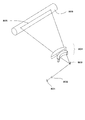
図15は、上記光偏向器を用いた光学機器の実施例を示す図である。ここでは、光学機器として画像形成装置を示している。図15において、803は本発明による光偏向器であり、本実施例では入射光を1次元に走査する。801はレーザ光源である。802はレンズ或いはレンズ群であり、804は書き込みレンズ或いはレンズ群である。805は感光体、806は走査軌跡である。
(Example 3)
FIG. 15 is a diagram showing an embodiment of an optical apparatus using the optical deflector. Here, an image forming apparatus is shown as an optical apparatus. In FIG. 15, 803 is an optical deflector according to the present invention, and in this embodiment, incident light is scanned one-dimensionally.
レーザ光源801から射出されたレーザ光は、光の偏向走査のタイミングと関係した所定の強度変調を受けて、光偏向器803により1次元に走査される。この走査されたレーザ光は、書き込みレンズ804により、感光体805上へ画像を形成する。感光体805は図示しない帯電器により一様に帯電されており、この上に光を走査することでその部分に静電潜像が形成される。次に、図示しない現像器により静電潜像の画像部分にトナー像が形成され、これを例えば図示しない用紙に転写・定着することで用紙上に画像が形成される。低い不良品率で作製できる本発明の光偏向器を利用した画像形成装置であるので、比較的安価に画像形成装置を提供できる。
The laser light emitted from the
本発明の光偏向器は、他の光学機器にも使用できて、これらの装置において、光源からの光ビームを偏向し、該光ビームの少なくとも一部を光照射対象物に入射させる。こうした光学機器としては、レーザビームプリンタなどの画像形成装置の他に、画像表示装置、バーコードリーダー等の光ビームを走査する機械装置などがある。 The light deflector of the present invention can be used for other optical devices. In these apparatuses, the light beam from the light source is deflected and at least a part of the light beam is incident on the light irradiation object. Examples of such optical equipment include an image display apparatus such as a laser beam printer, a mechanical apparatus that scans a light beam such as an image display apparatus, and a barcode reader.
100、300、500、600、700 単結晶シリコン基板
101、701、701a、701b、701e、701f 支持体の基本エッチングマスク
102a、102b、702a、702b 弾性支持部の基本エッチングマスク
103、303、503、603、703、703a、703b 可動部の基本エッチングマスク
107a、107b、107c、107d、307、507、607、707a、707b、707c、707d、707e、707f 可動部と連結している補正エッチングマスク
710a、710b、710c、710d、710e、710f 支持体と連結している補正エッチングマスク
151a、151b、151c、151d、351、751a、751b、751c、751d、751e、751f 強度低下部(補正エッチングマスクの貫通孔)
152a、152b、152c、152d、552、752a、752b、752c、752d 強度低下部(補正エッチングマスクの切れ込み)
153a、153b、153c、153d、653、753a、753b、753c、753d 強度低下部(補正エッチングマスクの薄肉部)
201 支持体
202a 202b 弾性支持部
203 可動部
204 光偏向素子(反射面)
205 駆動手段(永久磁石)
206 駆動手段(コイル)
207 揺動軸(ねじり軸)
801 光源(レーザ光源)
803 本発明の光偏向器
805 光照射対象物(感光体)
100, 300, 500, 600, 700 Monocrystalline silicon substrate
101, 701, 701a, 701b, 701e, 701f Support basic etching mask
102a, 102b, 702a, 702b Basic etching mask for elastic support
103, 303, 503, 603, 703, 703a, 703b Movable part basic etching mask
107a, 107b, 107c, 107d, 307, 507, 607, 707a, 707b, 707c, 707d, 707e, 707f Correction etching mask connected to the movable part
710a, 710b, 710c, 710d, 710e, 710f Correction etching mask connected to support
151a, 151b, 151c, 151d, 351, 751a, 751b, 751c, 751d, 751e, 751f Reduced strength portion (through hole of correction etching mask)
152a, 152b, 152c, 152d, 552, 752a, 752b, 752c, 752d Strength reduction part (cutting of correction etching mask)
153a, 153b, 153c, 153d, 653, 753a, 753b, 753c, 753d Strength reduction part (thin part of correction etching mask)
201 Support
202a 202b Elastic support
203 Moving parts
204 Optical deflection element (reflection surface)
205 Driving means (permanent magnet)
206 Drive means (coil)
207 Oscillating shaft (torsional shaft)
801 Light source (laser light source)
803 Optical deflector of the present invention
805 Light irradiation object (photoconductor)
Claims (11)
異方性エッチングにより、前記シリコン基板をエッチングして目標形状を形成する目標形状形成工程と、
を有し、
前記マスク形成工程において、局所的に機械的強度を低下させた強度低下部を前記補正エッチングマスクの連結部の少なくとも一部に形成することを特徴とする構造体の作製方法。 A mask forming step of forming a basic etching mask corresponding to a target shape and a correction etching mask having a connecting portion connected to the basic etching mask on a single crystal silicon substrate;
A target shape forming step of forming a target shape by etching the silicon substrate by anisotropic etching;
Have
In the mask formation step, a strength reduction portion in which mechanical strength is locally reduced is formed in at least a part of the connection portion of the correction etching mask.
前記基本エッチングマスクと前記補正エッチングマスクを有する前記単結晶シリコン基板を異方性エッチングし前記目標形状を形成する目標形状形成工程と、
を有し、
前記マスク形成工程において、前記第1の構造体の基本エッチングマスクと前記補正エッチングマスクとが連結する連結部の少なくとも一部に、局所的に機械的強度を低下させた強度低下部を形成することを特徴とする構造体の作製方法。 A basic etching mask corresponding to a target shape having at least a first structure having a convex corner and a second structure adjacent to the first structure via an opening on a single crystal silicon substrate; A mask forming step of forming a correction etching mask extending from a convex corner of the etching mask of the first structure and connecting with the etching mask of the second structure;
A target shape forming step of anisotropically etching the single crystal silicon substrate having the basic etching mask and the correction etching mask to form the target shape;
Have
In the mask forming step, a strength reduction portion in which mechanical strength is locally reduced is formed in at least a part of a connection portion where the basic etching mask of the first structure and the correction etching mask are connected. A method for manufacturing a structure characterized by the above.
局所的に機械的強度を低下させた強度低下部が、前記補正エッチングマスクの連結部の少なくとも一部に形成されていることを特徴とするエッチングマスク付きシリコン基板。 On a single crystal silicon substrate, a basic etching mask corresponding to a target shape, and a correction etching mask having a connecting portion connected to the basic etching mask,
A silicon substrate with an etching mask, characterized in that a strength-decreasing portion whose mechanical strength is locally reduced is formed in at least a part of the connecting portion of the correction etching mask.
請求項1乃至7のいずれか1項に記載の構造体の作製方法により作製されることを特徴とする揺動体装置。 A support, a movable part supported movably with respect to the support, an elastic support part elastically connecting the movable part to the support so as to swing about a swing axis, and the movable An oscillator device having a driving means for driving the unit,
8. An oscillator device produced by the method for producing a structure according to claim 1.
前記光偏向器が、光源からの光ビームを偏向し、該光ビームの少なくとも一部を光照射対象物に入射させることを特徴とする光学機器。 The optical deflector according to claim 10,
An optical apparatus, wherein the light deflector deflects a light beam from a light source and causes at least a part of the light beam to enter a light irradiation target.
Priority Applications (3)
| Application Number | Priority Date | Filing Date | Title |
|---|---|---|---|
| JP2007327510A JP2009148847A (en) | 2007-12-19 | 2007-12-19 | Manufacturing method for structure by anisotropic etching and silicon substrate with etching mask |
| US12/333,910 US20090161189A1 (en) | 2007-12-19 | 2008-12-12 | Method of manufacturing a structure based on anisotropic etching, and silicon substrate with etching mask |
| CN200810188516.8A CN101462692A (en) | 2007-12-19 | 2008-12-19 | Method of manufacturing a structure based on anisotropic etching, and silicon substrate with etching mask |
Applications Claiming Priority (1)
| Application Number | Priority Date | Filing Date | Title |
|---|---|---|---|
| JP2007327510A JP2009148847A (en) | 2007-12-19 | 2007-12-19 | Manufacturing method for structure by anisotropic etching and silicon substrate with etching mask |
Publications (2)
| Publication Number | Publication Date |
|---|---|
| JP2009148847A true JP2009148847A (en) | 2009-07-09 |
| JP2009148847A5 JP2009148847A5 (en) | 2011-02-10 |
Family
ID=40788273
Family Applications (1)
| Application Number | Title | Priority Date | Filing Date |
|---|---|---|---|
| JP2007327510A Withdrawn JP2009148847A (en) | 2007-12-19 | 2007-12-19 | Manufacturing method for structure by anisotropic etching and silicon substrate with etching mask |
Country Status (3)
| Country | Link |
|---|---|
| US (1) | US20090161189A1 (en) |
| JP (1) | JP2009148847A (en) |
| CN (1) | CN101462692A (en) |
Cited By (2)
| Publication number | Priority date | Publication date | Assignee | Title |
|---|---|---|---|---|
| US8614831B2 (en) | 2011-04-06 | 2013-12-24 | Seiko Epson Corporation | Actuator and optical scanner |
| US9293975B2 (en) | 2011-03-24 | 2016-03-22 | Seiko Epson Corporation | Actuator, optical scanner, and image forming apparatus |
Families Citing this family (3)
| Publication number | Priority date | Publication date | Assignee | Title |
|---|---|---|---|---|
| CN106767551A (en) * | 2016-11-18 | 2017-05-31 | 合肥工业大学 | The preparation method that a kind of micro-nano measuring apparatus use the highly sensitive elastic spring of high accuracy |
| DE102017217975A1 (en) * | 2017-10-10 | 2019-04-11 | Robert Bosch Gmbh | Micromechanical spring structure |
| JP7174634B2 (en) * | 2019-01-18 | 2022-11-17 | 東京エレクトロン株式会社 | Method for etching a film |
Family Cites Families (3)
| Publication number | Priority date | Publication date | Assignee | Title |
|---|---|---|---|---|
| US6803843B2 (en) * | 2001-02-22 | 2004-10-12 | Canon Kabushiki Kaisha | Movable-body apparatus, optical deflector, and method of fabricating the same |
| US6831765B2 (en) * | 2001-02-22 | 2004-12-14 | Canon Kabushiki Kaisha | Tiltable-body apparatus, and method of fabricating the same |
| JP3740444B2 (en) * | 2001-07-11 | 2006-02-01 | キヤノン株式会社 | Optical deflector, optical equipment using the same, torsional oscillator |
-
2007
- 2007-12-19 JP JP2007327510A patent/JP2009148847A/en not_active Withdrawn
-
2008
- 2008-12-12 US US12/333,910 patent/US20090161189A1/en not_active Abandoned
- 2008-12-19 CN CN200810188516.8A patent/CN101462692A/en active Pending
Cited By (2)
| Publication number | Priority date | Publication date | Assignee | Title |
|---|---|---|---|---|
| US9293975B2 (en) | 2011-03-24 | 2016-03-22 | Seiko Epson Corporation | Actuator, optical scanner, and image forming apparatus |
| US8614831B2 (en) | 2011-04-06 | 2013-12-24 | Seiko Epson Corporation | Actuator and optical scanner |
Also Published As
| Publication number | Publication date |
|---|---|
| US20090161189A1 (en) | 2009-06-25 |
| CN101462692A (en) | 2009-06-24 |
Similar Documents
| Publication | Publication Date | Title |
|---|---|---|
| US7719163B2 (en) | Actuator having fixed and movable comb electrodes | |
| JP2009128463A (en) | Method of manufacturing oscillating body apparatus, optical deflector composed of oscillating body apparatus manufactured by the method and optical equipment | |
| JP2009148847A (en) | Manufacturing method for structure by anisotropic etching and silicon substrate with etching mask | |
| US20100150612A1 (en) | Oscillator device and method of manufacturing the same | |
| JP4351586B2 (en) | Optical scanner having curved mirror and method for manufacturing the same | |
| JP6809018B2 (en) | Light deflector, light scanning device, image forming device and image projection device | |
| JP2008070863A (en) | Vibrating mirror, light writing device, and image forming apparatus | |
| JP5585478B2 (en) | MEMS element for optical deflection | |
| US8324113B2 (en) | Silicon processing method and silicon substrate with etching mask | |
| JP5147366B2 (en) | Method of manufacturing structure by anisotropic etching, and silicon substrate with etching mask | |
| JP2009031642A (en) | Rocking body device, light deflector and image forming apparatus using it | |
| US8081366B2 (en) | Oscillating device, light deflector, and image forming apparatus using the same | |
| JP5171489B2 (en) | Method of manufacturing structure by anisotropic etching, and silicon substrate with etching mask | |
| JP5353761B2 (en) | Manufacturing method of optical deflector | |
| JP2005279863A (en) | Manufacturing method of actuator and actuator | |
| JP2003315724A (en) | Vibrating mirror and method for manufacturing the same, optical scanner, and image forming device | |
| JP2006309098A (en) | Dimensional specification of mems scanning mirror with rib and tapered comb-teeth | |
| JP5624638B2 (en) | Silicon processing method and silicon substrate with etching mask | |
| JP2004198798A (en) | Oscillating body | |
| JP2007171780A (en) | Drive device and manufacturing method therefor, and display apparatus | |
| JP2015001543A (en) | Optical scanner, image display device, and head-mounted display | |
| JP7105934B2 (en) | MEMS mirror device and its manufacturing method | |
| JP2004347769A (en) | Oscillating mirror, optical write-in device and image forming apparatus | |
| JP6515638B2 (en) | Optical scanner, image display device and head mounted display | |
| JP2004252048A (en) | Vibration mirror, optical writing device and image forming device |
Legal Events
| Date | Code | Title | Description |
|---|---|---|---|
| A521 | Request for written amendment filed |
Free format text: JAPANESE INTERMEDIATE CODE: A523 Effective date: 20101217 |
|
| A621 | Written request for application examination |
Free format text: JAPANESE INTERMEDIATE CODE: A621 Effective date: 20101217 |
|
| A761 | Written withdrawal of application |
Free format text: JAPANESE INTERMEDIATE CODE: A761 Effective date: 20110624 |