JP2009147111A - 接合材、その製造方法および半導体装置 - Google Patents
接合材、その製造方法および半導体装置 Download PDFInfo
- Publication number
- JP2009147111A JP2009147111A JP2007322910A JP2007322910A JP2009147111A JP 2009147111 A JP2009147111 A JP 2009147111A JP 2007322910 A JP2007322910 A JP 2007322910A JP 2007322910 A JP2007322910 A JP 2007322910A JP 2009147111 A JP2009147111 A JP 2009147111A
- Authority
- JP
- Japan
- Prior art keywords
- bonding material
- layer
- melting point
- central layer
- bonding
- Prior art date
- Legal status (The legal status is an assumption and is not a legal conclusion. Google has not performed a legal analysis and makes no representation as to the accuracy of the status listed.)
- Pending
Links
Images


Classifications
-
- H—ELECTRICITY
- H01—ELECTRIC ELEMENTS
- H01L—SEMICONDUCTOR DEVICES NOT COVERED BY CLASS H10
- H01L24/00—Arrangements for connecting or disconnecting semiconductor or solid-state bodies; Methods or apparatus related thereto
- H01L24/01—Means for bonding being attached to, or being formed on, the surface to be connected, e.g. chip-to-package, die-attach, "first-level" interconnects; Manufacturing methods related thereto
- H01L24/26—Layer connectors, e.g. plate connectors, solder or adhesive layers; Manufacturing methods related thereto
- H01L24/28—Structure, shape, material or disposition of the layer connectors prior to the connecting process
- H01L24/29—Structure, shape, material or disposition of the layer connectors prior to the connecting process of an individual layer connector
-
- H—ELECTRICITY
- H01—ELECTRIC ELEMENTS
- H01L—SEMICONDUCTOR DEVICES NOT COVERED BY CLASS H10
- H01L2224/00—Indexing scheme for arrangements for connecting or disconnecting semiconductor or solid-state bodies and methods related thereto as covered by H01L24/00
- H01L2224/01—Means for bonding being attached to, or being formed on, the surface to be connected, e.g. chip-to-package, die-attach, "first-level" interconnects; Manufacturing methods related thereto
- H01L2224/26—Layer connectors, e.g. plate connectors, solder or adhesive layers; Manufacturing methods related thereto
- H01L2224/28—Structure, shape, material or disposition of the layer connectors prior to the connecting process
- H01L2224/29—Structure, shape, material or disposition of the layer connectors prior to the connecting process of an individual layer connector
- H01L2224/29001—Core members of the layer connector
- H01L2224/29075—Plural core members
- H01L2224/2908—Plural core members being stacked
- H01L2224/29083—Three-layer arrangements
-
- H—ELECTRICITY
- H01—ELECTRIC ELEMENTS
- H01L—SEMICONDUCTOR DEVICES NOT COVERED BY CLASS H10
- H01L2224/00—Indexing scheme for arrangements for connecting or disconnecting semiconductor or solid-state bodies and methods related thereto as covered by H01L24/00
- H01L2224/01—Means for bonding being attached to, or being formed on, the surface to be connected, e.g. chip-to-package, die-attach, "first-level" interconnects; Manufacturing methods related thereto
- H01L2224/26—Layer connectors, e.g. plate connectors, solder or adhesive layers; Manufacturing methods related thereto
- H01L2224/28—Structure, shape, material or disposition of the layer connectors prior to the connecting process
- H01L2224/29—Structure, shape, material or disposition of the layer connectors prior to the connecting process of an individual layer connector
- H01L2224/29001—Core members of the layer connector
- H01L2224/29099—Material
- H01L2224/291—Material with a principal constituent of the material being a metal or a metalloid, e.g. boron [B], silicon [Si], germanium [Ge], arsenic [As], antimony [Sb], tellurium [Te] and polonium [Po], and alloys thereof
- H01L2224/29101—Material with a principal constituent of the material being a metal or a metalloid, e.g. boron [B], silicon [Si], germanium [Ge], arsenic [As], antimony [Sb], tellurium [Te] and polonium [Po], and alloys thereof the principal constituent melting at a temperature of less than 400°C
- H01L2224/29111—Tin [Sn] as principal constituent
-
- H—ELECTRICITY
- H01—ELECTRIC ELEMENTS
- H01L—SEMICONDUCTOR DEVICES NOT COVERED BY CLASS H10
- H01L2224/00—Indexing scheme for arrangements for connecting or disconnecting semiconductor or solid-state bodies and methods related thereto as covered by H01L24/00
- H01L2224/01—Means for bonding being attached to, or being formed on, the surface to be connected, e.g. chip-to-package, die-attach, "first-level" interconnects; Manufacturing methods related thereto
- H01L2224/26—Layer connectors, e.g. plate connectors, solder or adhesive layers; Manufacturing methods related thereto
- H01L2224/28—Structure, shape, material or disposition of the layer connectors prior to the connecting process
- H01L2224/29—Structure, shape, material or disposition of the layer connectors prior to the connecting process of an individual layer connector
- H01L2224/29001—Core members of the layer connector
- H01L2224/29099—Material
- H01L2224/291—Material with a principal constituent of the material being a metal or a metalloid, e.g. boron [B], silicon [Si], germanium [Ge], arsenic [As], antimony [Sb], tellurium [Te] and polonium [Po], and alloys thereof
- H01L2224/29101—Material with a principal constituent of the material being a metal or a metalloid, e.g. boron [B], silicon [Si], germanium [Ge], arsenic [As], antimony [Sb], tellurium [Te] and polonium [Po], and alloys thereof the principal constituent melting at a temperature of less than 400°C
- H01L2224/29113—Bismuth [Bi] as principal constituent
-
- H—ELECTRICITY
- H01—ELECTRIC ELEMENTS
- H01L—SEMICONDUCTOR DEVICES NOT COVERED BY CLASS H10
- H01L2224/00—Indexing scheme for arrangements for connecting or disconnecting semiconductor or solid-state bodies and methods related thereto as covered by H01L24/00
- H01L2224/01—Means for bonding being attached to, or being formed on, the surface to be connected, e.g. chip-to-package, die-attach, "first-level" interconnects; Manufacturing methods related thereto
- H01L2224/26—Layer connectors, e.g. plate connectors, solder or adhesive layers; Manufacturing methods related thereto
- H01L2224/28—Structure, shape, material or disposition of the layer connectors prior to the connecting process
- H01L2224/29—Structure, shape, material or disposition of the layer connectors prior to the connecting process of an individual layer connector
- H01L2224/29001—Core members of the layer connector
- H01L2224/29099—Material
- H01L2224/291—Material with a principal constituent of the material being a metal or a metalloid, e.g. boron [B], silicon [Si], germanium [Ge], arsenic [As], antimony [Sb], tellurium [Te] and polonium [Po], and alloys thereof
- H01L2224/29117—Material with a principal constituent of the material being a metal or a metalloid, e.g. boron [B], silicon [Si], germanium [Ge], arsenic [As], antimony [Sb], tellurium [Te] and polonium [Po], and alloys thereof the principal constituent melting at a temperature of greater than or equal to 400°C and less than 950°C
- H01L2224/29118—Zinc [Zn] as principal constituent
-
- H—ELECTRICITY
- H01—ELECTRIC ELEMENTS
- H01L—SEMICONDUCTOR DEVICES NOT COVERED BY CLASS H10
- H01L2224/00—Indexing scheme for arrangements for connecting or disconnecting semiconductor or solid-state bodies and methods related thereto as covered by H01L24/00
- H01L2224/01—Means for bonding being attached to, or being formed on, the surface to be connected, e.g. chip-to-package, die-attach, "first-level" interconnects; Manufacturing methods related thereto
- H01L2224/26—Layer connectors, e.g. plate connectors, solder or adhesive layers; Manufacturing methods related thereto
- H01L2224/31—Structure, shape, material or disposition of the layer connectors after the connecting process
- H01L2224/32—Structure, shape, material or disposition of the layer connectors after the connecting process of an individual layer connector
- H01L2224/321—Disposition
- H01L2224/32151—Disposition the layer connector connecting between a semiconductor or solid-state body and an item not being a semiconductor or solid-state body, e.g. chip-to-substrate, chip-to-passive
- H01L2224/32221—Disposition the layer connector connecting between a semiconductor or solid-state body and an item not being a semiconductor or solid-state body, e.g. chip-to-substrate, chip-to-passive the body and the item being stacked
- H01L2224/32225—Disposition the layer connector connecting between a semiconductor or solid-state body and an item not being a semiconductor or solid-state body, e.g. chip-to-substrate, chip-to-passive the body and the item being stacked the item being non-metallic, e.g. insulating substrate with or without metallisation
-
- H—ELECTRICITY
- H01—ELECTRIC ELEMENTS
- H01L—SEMICONDUCTOR DEVICES NOT COVERED BY CLASS H10
- H01L2224/00—Indexing scheme for arrangements for connecting or disconnecting semiconductor or solid-state bodies and methods related thereto as covered by H01L24/00
- H01L2224/01—Means for bonding being attached to, or being formed on, the surface to be connected, e.g. chip-to-package, die-attach, "first-level" interconnects; Manufacturing methods related thereto
- H01L2224/42—Wire connectors; Manufacturing methods related thereto
- H01L2224/44—Structure, shape, material or disposition of the wire connectors prior to the connecting process
- H01L2224/45—Structure, shape, material or disposition of the wire connectors prior to the connecting process of an individual wire connector
- H01L2224/45001—Core members of the connector
- H01L2224/45099—Material
- H01L2224/451—Material with a principal constituent of the material being a metal or a metalloid, e.g. boron (B), silicon (Si), germanium (Ge), arsenic (As), antimony (Sb), tellurium (Te) and polonium (Po), and alloys thereof
- H01L2224/45117—Material with a principal constituent of the material being a metal or a metalloid, e.g. boron (B), silicon (Si), germanium (Ge), arsenic (As), antimony (Sb), tellurium (Te) and polonium (Po), and alloys thereof the principal constituent melting at a temperature of greater than or equal to 400°C and less than 950°C
- H01L2224/45124—Aluminium (Al) as principal constituent
-
- H—ELECTRICITY
- H01—ELECTRIC ELEMENTS
- H01L—SEMICONDUCTOR DEVICES NOT COVERED BY CLASS H10
- H01L2224/00—Indexing scheme for arrangements for connecting or disconnecting semiconductor or solid-state bodies and methods related thereto as covered by H01L24/00
- H01L2224/01—Means for bonding being attached to, or being formed on, the surface to be connected, e.g. chip-to-package, die-attach, "first-level" interconnects; Manufacturing methods related thereto
- H01L2224/42—Wire connectors; Manufacturing methods related thereto
- H01L2224/47—Structure, shape, material or disposition of the wire connectors after the connecting process
- H01L2224/48—Structure, shape, material or disposition of the wire connectors after the connecting process of an individual wire connector
- H01L2224/4805—Shape
- H01L2224/4809—Loop shape
- H01L2224/48091—Arched
-
- H—ELECTRICITY
- H01—ELECTRIC ELEMENTS
- H01L—SEMICONDUCTOR DEVICES NOT COVERED BY CLASS H10
- H01L2224/00—Indexing scheme for arrangements for connecting or disconnecting semiconductor or solid-state bodies and methods related thereto as covered by H01L24/00
- H01L2224/01—Means for bonding being attached to, or being formed on, the surface to be connected, e.g. chip-to-package, die-attach, "first-level" interconnects; Manufacturing methods related thereto
- H01L2224/42—Wire connectors; Manufacturing methods related thereto
- H01L2224/47—Structure, shape, material or disposition of the wire connectors after the connecting process
- H01L2224/48—Structure, shape, material or disposition of the wire connectors after the connecting process of an individual wire connector
- H01L2224/481—Disposition
- H01L2224/48151—Connecting between a semiconductor or solid-state body and an item not being a semiconductor or solid-state body, e.g. chip-to-substrate, chip-to-passive
- H01L2224/48221—Connecting between a semiconductor or solid-state body and an item not being a semiconductor or solid-state body, e.g. chip-to-substrate, chip-to-passive the body and the item being stacked
- H01L2224/48225—Connecting between a semiconductor or solid-state body and an item not being a semiconductor or solid-state body, e.g. chip-to-substrate, chip-to-passive the body and the item being stacked the item being non-metallic, e.g. insulating substrate with or without metallisation
- H01L2224/48227—Connecting between a semiconductor or solid-state body and an item not being a semiconductor or solid-state body, e.g. chip-to-substrate, chip-to-passive the body and the item being stacked the item being non-metallic, e.g. insulating substrate with or without metallisation connecting the wire to a bond pad of the item
-
- H—ELECTRICITY
- H01—ELECTRIC ELEMENTS
- H01L—SEMICONDUCTOR DEVICES NOT COVERED BY CLASS H10
- H01L2224/00—Indexing scheme for arrangements for connecting or disconnecting semiconductor or solid-state bodies and methods related thereto as covered by H01L24/00
- H01L2224/73—Means for bonding being of different types provided for in two or more of groups H01L2224/10, H01L2224/18, H01L2224/26, H01L2224/34, H01L2224/42, H01L2224/50, H01L2224/63, H01L2224/71
- H01L2224/732—Location after the connecting process
- H01L2224/73251—Location after the connecting process on different surfaces
- H01L2224/73265—Layer and wire connectors
-
- H—ELECTRICITY
- H01—ELECTRIC ELEMENTS
- H01L—SEMICONDUCTOR DEVICES NOT COVERED BY CLASS H10
- H01L2224/00—Indexing scheme for arrangements for connecting or disconnecting semiconductor or solid-state bodies and methods related thereto as covered by H01L24/00
- H01L2224/80—Methods for connecting semiconductor or other solid state bodies using means for bonding being attached to, or being formed on, the surface to be connected
- H01L2224/83—Methods for connecting semiconductor or other solid state bodies using means for bonding being attached to, or being formed on, the surface to be connected using a layer connector
- H01L2224/831—Methods for connecting semiconductor or other solid state bodies using means for bonding being attached to, or being formed on, the surface to be connected using a layer connector the layer connector being supplied to the parts to be connected in the bonding apparatus
- H01L2224/83101—Methods for connecting semiconductor or other solid state bodies using means for bonding being attached to, or being formed on, the surface to be connected using a layer connector the layer connector being supplied to the parts to be connected in the bonding apparatus as prepeg comprising a layer connector, e.g. provided in an insulating plate member
-
- H—ELECTRICITY
- H01—ELECTRIC ELEMENTS
- H01L—SEMICONDUCTOR DEVICES NOT COVERED BY CLASS H10
- H01L2924/00—Indexing scheme for arrangements or methods for connecting or disconnecting semiconductor or solid-state bodies as covered by H01L24/00
- H01L2924/30—Technical effects
- H01L2924/35—Mechanical effects
- H01L2924/351—Thermal stress
Abstract
【課題】接合性が被接合材に関わらず良好で、高温耐量の高い接合材を提供すること。また、この接合材を用いて接合された半導体装置の耐熱性を向上させること。
【解決手段】融点が、たとえば260℃以上と高い板状の中央層2の上下表面に、中央層2より融点が低く濡れ性の良好な表面層3を積層することで接合材1を得ることができる。また、この接合材1を介して半導体チップや絶縁基板などの被接合材を接合することで半導体装置を形成する。
【選択図】図1
【解決手段】融点が、たとえば260℃以上と高い板状の中央層2の上下表面に、中央層2より融点が低く濡れ性の良好な表面層3を積層することで接合材1を得ることができる。また、この接合材1を介して半導体チップや絶縁基板などの被接合材を接合することで半導体装置を形成する。
【選択図】図1
Description
この発明は、接合性が良好で融点が高い接合材、その製造方法およびこの接合材を用いて接合された半導体装置に関する。
従来、パワーデバイスは、電力変換用途のスイッチングデバイスとして用いられる。図3は、従来の半導体装置の構造について示す断面図である。図3に示すように、半導体装置10は、半導体チップ11と、配線基板12と、アルミワイヤ13と、ヒートシンク14と、ケース15と、を備えている。
配線基板12は、絶縁基板の表面に回路パターン12a,12bを形成した基板である。半導体チップ11の裏面は、図示省略した接合材を介して配線基板12の回路パターン12aと接合している。半導体チップ11の表面に設けられた図示省略した電極と回路パターン12bとはアルミワイヤ13によって電気的に接続されている。配線基板12の裏面には金属膜12cが設けられており、この金属膜12cが図示を省略した接合材を介してヒートシンク14と接合している。
ヒートシンク14は、良熱伝導体の材質で作られており、ベース部14aおよび放熱フィン部14bを有する。ベース部14aは、半導体チップ11で発生し、配線基板12を介して伝わる熱を放熱フィン部14bへ伝導する。放熱フィン部14bは、複数の放熱フィンを有し、ベース部14aから伝導された熱を放散する。ヒートシンク14の周縁にはケース15が接着されている。
上述したモジュール構造の半導体装置10では、半導体チップ11と絶縁基板12の表面に形成された回路パターン12aとの接合に、接合材として、比較的低い融点で固着工程をおこなえる半田が用いられている。このように、接合材として用いられる半田材は、実装を容易にすることはできるが、融点が200〜300℃程度である。したがって、半導体装置の動作寿命を推定する実機動作試験(パワーサイクル試験)などにより、半田層の内部に発生する亀裂が進展し、半導体装置の機能を喪失させることがある(たとえば、下記非特許文献1参照。)。
半田層の内部に発生する亀裂が進展する原因の一つは、半導体チップ11の素材であるシリコンの熱膨張係数(α≒3.0ppm/k)と、回路パターン12aの素材である、たとえば銅の熱膨張係数(α≒18.0ppm/k)と、が異なることによって熱応力が生じることである。また、特に錫(Sn)を多く含有し、鉛(Pb)を含有しない半田(以下、Pbフリー半田とする)においては、半田材の再結晶化によって組織の変化が起こり、半田層の内部に発生する亀裂が進展する。この組織変化の時間的な進行速度は、半田材の高温耐量と強い相関を有することが知られている。したがって、半導体装置を高温で安定して動作させるためには、接合材のさらなる高温耐量化が求められている。
また、図3に示す半導体装置は積層構造を有しており、放熱性を向上させるために面接合構造となっている。したがって、半導体装置に用いられる接合材には、構造の信頼性を確保するための高耐熱性と、実装をおこなうための接合性と、が必要とされる。半導体装置の製造工程の接合処理においては、還元炉などに通して、被接合材(部材)に挟まれた接合材が溶融することによって接合が進行する。また、還元炉の還元力の強弱により、箔形状または粉体にフラックスを融合したペースト形状の接合材が用いられる。箔形状の接合材の接合性は、還元炉内の雰囲気(たとえば、水素置換雰囲気などによる還元力)、溶融した金属の濡れ性および被接合材との組み合わせによる活性傾向により決定する。
ここで、接合材として錫(Sn)と亜鉛(Zn)の混合材(融点温度:160〜180℃)などの酸化傾向が強く濡れ性の悪い低温接合材を線形状にし、このSn−Zn混合材を濡れ性が良好で異なる組成の膜で被うことによって、半田付け温度を低くして、実装をおこなうための接合性を向上させた接合材が提案されている(たとえば、下記特許文献1参照。)。
また、一般に、Pbが含有されていない接合材としては、融点範囲が210〜240℃程度の、Snを多く含有するPbフリー半田が用いられているが、Pbを多く含有する高温半田の代替えとなる温度領域のものが必要とされている。最近では、融点範囲が約260℃以上である、ビスマス(Bi)組成の合金系の接合材が注目されている。なお、Biは、単相状態では融点が271℃である(たとえば、下記特許文献2または下記非特許文献2参照。)。
しかしながら、上述した特許文献1の技術では、接合材の融点が低いため、この接合材を用いて接合した半導体装置の耐熱性を向上させることができないという問題がある。一方、特許文献2または非特許文献2の技術では、Bi組成の合金系の接合材は、Snを多く含有するPbフリー半田と異なり、被接合材の材質との組み合わせによって、接合性の品質に顕著な差異が生じるという問題がある。また、実装の際の濡れ性が劣っているため、面接合構造の製品に適用するのが困難であるという問題がある。
この発明は、上述した従来技術による問題点を解消するため、接合性が被接合材に関わらず良好で、高温耐量の高い接合材およびその製造方法と、この接合材を用いて接合された半導体装置を提供することを目的とする。
上述した課題を解決し、目的を達成するため、請求項1の発明にかかる接合材は、板状の中央層の上下表面に表面層が積層された接合材であって、前記中央層は前記表面層より融点が高いことを特徴とする。
また、請求項2の発明にかかる接合材は、請求項1に記載の発明において、少なくとも、前記中央層と当該中央層の上下表面に積層された前記表面層との3層で形成されたことを特徴とする。
また、請求項3の発明にかかる接合材は、請求項1または2に記載の発明において、前記中央層は、融点が260℃以上であることを特徴とする。
また、請求項4の発明にかかる接合材は、請求項1〜3のいずれか一つに記載の発明において、前記中央層は、ビスマスの単相、またはビスマスを主成分とする、銀、銅、亜鉛、アンチモン、インジウム、錫、ニッケル、ゲルマニウム、テルル、リンなどとの合金からなることを特徴とする。
また、請求項5の発明にかかる接合材は、請求項1〜4のいずれか一つに記載の発明において、前記表面層は、錫の単相、インジウムの単相、または錫もしくはインジウムを主成分とする合金からなることを特徴とする。
また、請求項6の発明にかかる接合材の製造方法は、板状の中央層の上下表面に、当該中央層より融点の低い表面層を積層する積層工程と、前記中央層および前記表面層を、圧延することで一体化する圧延工程と、を含むことを特徴とする。
また、請求項7の発明にかかる接合材の製造方法は、板状の中央層の上下表面に、当該中央層より融点の低い表面層を、電鋳による膜形成によって形成することを特徴とする。
また、請求項8の発明にかかる接合材の製造方法は、板状の中央層の上下表面に、当該中央層より融点の低い表面層を、微細な粉体粒子を噴霧することで形成することを特徴とする。
また、請求項9の発明にかかる半導体装置は、前記1〜5に記載の接合材を用いて半導体チップと絶縁基板とが接合されたことを特徴とする。
上述の各発明によれば、融点の高い中央層の上下表面に、中央層より濡れ性が良好で中央層より融点の低い表面層が積層された接合材を得ることができる。このため、被接合材に挟まれた接合材に熱を加えると、中央層より先に、濡れ性の良好な表面層が溶融し、被接合材の表面と反応することで、固−液相界面を形成する。また、中央層の融点が260℃以上と高いため、接合材の高温耐量が向上する。
本発明にかかる接合材、その製造方法によれば、接合性が被接合材に関わらず良好で、高温耐量の高い接合材を提供することができる。また、この接合材を用いて接合された半導体装置の耐熱性を向上させることができるという効果を奏する。
以下に添付図面を参照して、この発明にかかる接合材、その製造方法およびこの接合材を用いて接合された半導体装置の好適な実施の形態を詳細に説明する。なお、以下の実施の形態の説明およびすべての添付図面において、同様の構成には同一の符号を付し、重複する説明を省略する。
(実施の形態)
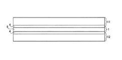
図1は、本実施の形態にかかる接合材の構造を示す断面図である。図1に示すように、本実施の形態にかかる接合材1は、板状に個片化された圧延材である。接合材1は、たとえば、ビスマス(Bi)が多く含有された中央層2のおもて面と裏面に、表面層3が積層されている。
図1は、本実施の形態にかかる接合材の構造を示す断面図である。図1に示すように、本実施の形態にかかる接合材1は、板状に個片化された圧延材である。接合材1は、たとえば、ビスマス(Bi)が多く含有された中央層2のおもて面と裏面に、表面層3が積層されている。
ここで、中央層2は、たとえば、融点が260℃以上の高融点の材質である。具体的には、Biを主成分として、銀(Ag)、銅(Cu)、亜鉛(Zn)、アンチモン(Sb)、インジウム(In)、錫(Sn)、ニッケル(Ni)、ゲルマニウム(Ge)、テルル(Te)、リン(P)等を添加した合金が好適であり、さらに具体的には、融点が260℃以上の、Bi、Bi−Ag、Bi−Cu系の2元組成の合金が材質として好ましい。または、融点が380℃以上のZn−Al系合金が材質として好ましい。
Bi系合金を中央層2とする場合、100Biは融点が271℃となる。また、Bi−Ag系合金を中央層2とする場合、組成がBi−2.5Agで融点が260℃程度と最小となる。また、Bi−Cu系合金を中央層2とする場合、組成がBi−0.5Cuで融点が260℃と最小となる。さらに、Zn−Al系合金を中央層2とする場合、組成がZn−6.0〜8.0Alで融点が370℃程度と最小となる。
また、表面層3は、Pbが含有されず、融点が260℃未満である材質が好ましい。たとえば、マクロな濡れ性を有するSnまたはInなどの単相材、もしくは、これらSn、Inと、電子材料として電極に用いられるCu、NiまたはAgなどの表面材との合金が好適である。具体的には、Sn−3.5Ag、Sn−3.0Ag−0.5Cu、Sn−8.0Zn−0.5Cu、100In、95In−5.0Sb等である。
つぎに、接合材の製造方法について説明する。図1に示すように、中央層2の上下表面に表面層3を積層し、冷間または温間で圧延し、板状のペレット材にすることで接合材1を形成する。また、この表面層3を、中央層2の上下の最表面に成膜することで形成してもよい。たとえば、スパッタ、電解または無電解などのめっき処理によって表面層3を成膜してもよいし、一般に用いられているめっき材質である半田めっき(SnまたはSn−Agを含有し、Pbを含まないめっき)を施して表面層3を成膜してもよい。
図2は、図1に示す接合材を用いて接合された半導体装置について示す断面図である。図2に示すように、図1に示す接合材1が、被接合材である半導体チップ11と絶縁基板12とによって挟まれた状態となっている。また、半導体チップ11および絶縁基板12と接合材1の接合界面付近に形成された反応相4は、接合材1の最表面と被接合材の最表面とが、液相−固相反応によって一体化して形成された反応層4である。また、接合材1の内部はバルク層5となる。
つぎに、半導体装置を図1に示す接合材を用いて接合する方法について説明する。接合材1が半導体チップ11および絶縁基板12に挟まれた状態のまま、還元炉に通し、接合材1と、半導体チップ11および絶縁基板12とを還元雰囲気で加熱溶融させて、接合する。加熱温度は、接合材1、半導体チップ11および絶縁基板12の表面が還元雰囲気内で還元される温度であり、たとえば、接合材1の中央層の融点より30〜40℃高い温度が好ましい。
たとえば、中央層が100Bi(融点:271℃)の場合、通常の水素雰囲気内であれば中央層の表面が十分に還元されるため、310〜320℃程度に加熱することで全体の溶融一体化が進行する。ここで、表面層がSn(融点:230℃)の場合、加熱処理の途中で、中央層よりも融点の低い表面層が先に溶融し、表面層と被接合材の表面が反応し、固−液相界面が形成される。
被接合材である半導体チップ11の最表面には、銅めっきなどの再配線層またはスパッタや蒸着などによるメタライズ層(Ni−Au、Ni−Ag等)が形成されている。また、絶縁基板12の最表面にも、成膜工程は異なるが、同様の層が形成されていることが多い。そして、これら被接合材におけるNi、Cu、Ag、Auなどの固相を保った表面と溶融した表面層3とによって、固−液相の境界を通して化学反応物が生成されることで、反応層4が形成される。
本実施の形態によれば、被接合材の表面と接合材の表面層とによって生成される化学反応物は、被接合材の表面と従来のSnを多く含有するPbフリー半田とによって生成される化学反応物と同様のものである。したがって、Snを多く含有するPbフリー半田と同様の接合性であることがわかる。また、接合材の表面層が溶融し、被接合材に流動する時の濡れ性が、接合材の中央層よりも優れており、被接合材との接合欠陥を避けることができる。このため、接合材の接合性が向上するため、緻密な面接合領域を形成することができる。これにより、面接合形式の被接合材の接合材として接合品質を向上させることができる。さらに、接合材の中央層の融点が、たとえば、260℃以上と高く、接合材の高温耐量を高くすることができるため、この接合材を用いて接合された半導体装置の耐熱性を向上させることができる。
なお、本実施の形態においては、中央層をBi系合金の材質とし、表面層をSn系合金の材質として説明したが、中央層の融点が高温(たとえば、260℃以上)であり、表面層の界面接合性が良好な材質であれば、これに限るものではない。
また、本実施の形態においては、中央層と、この中央層の上下表面に積層された表面層の3層構造について説明したが、少なくとも3層構造であればよく、中央層や表面層が複数の層からなる構造でもよい。
以上のように、本発明にかかる接合材、その製造方法および半導体装置は、高温で動作するパワーデバイスに有用であり、特に、電力変換用途のスイッチングデバイスに適している。
1 接合材
2 中央層
3 表面層
2 中央層
3 表面層
Claims (9)
- 板状の中央層の上下表面に表面層が積層された接合材であって、前記中央層は前記表面層より融点が高いことを特徴とする接合材。
- 少なくとも、前記中央層と当該中央層の上下表面に積層された前記表面層との3層で形成されたことを特徴とする請求項1に記載の接合材。
- 前記中央層は、融点が260℃以上であることを特徴とする請求項1または2に記載の接合材。
- 前記中央層は、ビスマスの単相、またはビスマスを主成分とする、銀、銅、亜鉛、アンチモン、インジウム、錫、ニッケル、ゲルマニウム、テルル、リンなどとの合金からなることを特徴とする請求項1〜3のいずれか一つに記載の接合材。
- 前記表面層は、錫の単相、インジウムの単相、または錫もしくはインジウムを主成分とする合金からなることを特徴とする請求項1〜4のいずれか一つに記載の接合材。
- 板状の中央層の上下表面に、当該中央層より融点の低い表面層を積層する積層工程と、
前記中央層および前記表面層を、圧延することで一体化する圧延工程と、
を含むことを特徴とする接合材の製造方法。 - 板状の中央層の上下表面に、当該中央層より融点の低い表面層を、電鋳による膜形成によって形成することを特徴とする接合材の製造方法。
- 板状の中央層の上下表面に、当該中央層より融点の低い表面層を、微細な粉体粒子を噴霧することで形成することを特徴とする接合材の製造方法。
- 前記1〜5のいずれか一つに記載の接合材を用いて半導体チップと絶縁基板とが接合されたことを特徴とする半導体装置。
Priority Applications (1)
| Application Number | Priority Date | Filing Date | Title |
|---|---|---|---|
| JP2007322910A JP2009147111A (ja) | 2007-12-14 | 2007-12-14 | 接合材、その製造方法および半導体装置 |
Applications Claiming Priority (1)
| Application Number | Priority Date | Filing Date | Title |
|---|---|---|---|
| JP2007322910A JP2009147111A (ja) | 2007-12-14 | 2007-12-14 | 接合材、その製造方法および半導体装置 |
Publications (1)
| Publication Number | Publication Date |
|---|---|
| JP2009147111A true JP2009147111A (ja) | 2009-07-02 |
Family
ID=40917384
Family Applications (1)
| Application Number | Title | Priority Date | Filing Date |
|---|---|---|---|
| JP2007322910A Pending JP2009147111A (ja) | 2007-12-14 | 2007-12-14 | 接合材、その製造方法および半導体装置 |
Country Status (1)
| Country | Link |
|---|---|
| JP (1) | JP2009147111A (ja) |
Cited By (10)
| Publication number | Priority date | Publication date | Assignee | Title |
|---|---|---|---|---|
| JP2009269075A (ja) * | 2008-05-09 | 2009-11-19 | Sumitomo Metal Mining Co Ltd | 応力緩和層を有する積層はんだ材の製造方法および製造装置 |
| WO2011036829A1 (ja) * | 2009-09-24 | 2011-03-31 | パナソニック株式会社 | 半導体装置及びその製造方法 |
| WO2011125140A1 (ja) * | 2010-04-05 | 2011-10-13 | 株式会社日立製作所 | 接続材料半導体装置及びその製造方法 |
| JP2012099465A (ja) * | 2010-10-29 | 2012-05-24 | General Electric Co <Ge> | ターゲットと軸受スリーブとを結合したx線管 |
| WO2012164865A1 (ja) * | 2011-06-03 | 2012-12-06 | パナソニック株式会社 | 接合構造体 |
| JPWO2012053178A1 (ja) * | 2010-10-22 | 2014-02-24 | パナソニック株式会社 | 半導体接合構造体および半導体接合構造体の製造方法 |
| JP2014136236A (ja) * | 2013-01-16 | 2014-07-28 | Sumitomo Metal Mining Co Ltd | PbフリーIn系はんだ合金 |
| JP6871524B1 (ja) * | 2020-03-23 | 2021-05-12 | 千住金属工業株式会社 | 積層接合材料、半導体パッケージおよびパワーモジュール |
| WO2022230697A1 (ja) | 2021-04-28 | 2022-11-03 | 千住金属工業株式会社 | 積層接合材料、半導体パッケージおよびパワーモジュール |
| JP2022549450A (ja) * | 2019-10-23 | 2022-11-25 | アルファ・アセンブリー・ソリューションズ・インコーポレイテッド | 電子アセンブリのための工学材料 |
-
2007
- 2007-12-14 JP JP2007322910A patent/JP2009147111A/ja active Pending
Cited By (19)
| Publication number | Priority date | Publication date | Assignee | Title |
|---|---|---|---|---|
| JP2009269075A (ja) * | 2008-05-09 | 2009-11-19 | Sumitomo Metal Mining Co Ltd | 応力緩和層を有する積層はんだ材の製造方法および製造装置 |
| WO2011036829A1 (ja) * | 2009-09-24 | 2011-03-31 | パナソニック株式会社 | 半導体装置及びその製造方法 |
| WO2011125140A1 (ja) * | 2010-04-05 | 2011-10-13 | 株式会社日立製作所 | 接続材料半導体装置及びその製造方法 |
| JP2011218364A (ja) * | 2010-04-05 | 2011-11-04 | Hitachi Ltd | 接続材料半導体装置及びその製造方法 |
| JPWO2012053178A1 (ja) * | 2010-10-22 | 2014-02-24 | パナソニック株式会社 | 半導体接合構造体および半導体接合構造体の製造方法 |
| JP5546067B2 (ja) * | 2010-10-22 | 2014-07-09 | パナソニック株式会社 | 半導体接合構造体および半導体接合構造体の製造方法 |
| JP2012099465A (ja) * | 2010-10-29 | 2012-05-24 | General Electric Co <Ge> | ターゲットと軸受スリーブとを結合したx線管 |
| WO2012164865A1 (ja) * | 2011-06-03 | 2012-12-06 | パナソニック株式会社 | 接合構造体 |
| JP2014136236A (ja) * | 2013-01-16 | 2014-07-28 | Sumitomo Metal Mining Co Ltd | PbフリーIn系はんだ合金 |
| JP2022549450A (ja) * | 2019-10-23 | 2022-11-25 | アルファ・アセンブリー・ソリューションズ・インコーポレイテッド | 電子アセンブリのための工学材料 |
| JP6871524B1 (ja) * | 2020-03-23 | 2021-05-12 | 千住金属工業株式会社 | 積層接合材料、半導体パッケージおよびパワーモジュール |
| JP2021150559A (ja) * | 2020-03-23 | 2021-09-27 | 千住金属工業株式会社 | 積層接合材料、半導体パッケージおよびパワーモジュール |
| WO2021193420A1 (ja) | 2020-03-23 | 2021-09-30 | 千住金属工業株式会社 | 積層接合材料、半導体パッケージおよびパワーモジュール |
| KR20220123723A (ko) * | 2020-03-23 | 2022-09-08 | 센주긴조쿠고교 가부시키가이샤 | 적층 접합 재료, 반도체 패키지 및 파워 모듈 |
| KR102454265B1 (ko) | 2020-03-23 | 2022-10-14 | 센주긴조쿠고교 가부시키가이샤 | 적층 접합 재료, 반도체 패키지 및 파워 모듈 |
| TWI807282B (zh) * | 2020-03-23 | 2023-07-01 | 日商千住金屬工業股份有限公司 | 積層接合材料、半導體封裝及功率模組 |
| US11712760B2 (en) | 2020-03-23 | 2023-08-01 | Senju Metal Industry Co., Ltd. | Layered bonding material, semiconductor package, and power module |
| EP4071257A4 (en) * | 2020-03-23 | 2023-11-29 | Senju Metal Industry Co., Ltd. | LAYERED BONDING MATERIAL, SEMICONDUCTOR PACKAGE AND POWER MODULE |
| WO2022230697A1 (ja) | 2021-04-28 | 2022-11-03 | 千住金属工業株式会社 | 積層接合材料、半導体パッケージおよびパワーモジュール |
Similar Documents
| Publication | Publication Date | Title |
|---|---|---|
| JP2009147111A (ja) | 接合材、その製造方法および半導体装置 | |
| JP6111764B2 (ja) | パワーモジュール用基板の製造方法 | |
| TWI641300B (zh) | 接合體及功率模組用基板 | |
| JP5672324B2 (ja) | 接合体の製造方法及びパワーモジュール用基板の製造方法 | |
| Suganuma et al. | Ultra heat-shock resistant die attachment for silicon carbide with pure zinc | |
| JP7198224B2 (ja) | 拡散はんだ付けのための無鉛はんだ膜及びその製造のための方法 | |
| JP6281468B2 (ja) | 半導体装置とその製造方法 | |
| JP2007281412A (ja) | パワー半導体モジュール | |
| CN109755208B (zh) | 一种接合材料、半导体装置及其制造方法 | |
| CN112338387A (zh) | 半导体装置用软钎焊材料 | |
| US10370303B2 (en) | Process for producing bonded body and process for producing power module substrate | |
| TWI529880B (zh) | 半導體元件,半導體封裝結構及其製造方法 | |
| WO2018168858A1 (ja) | はんだ材 | |
| JP2009129983A (ja) | 接合体及びその製造方法、並びにパワー半導体モジュール及びその製造方法 | |
| JP2012119609A (ja) | 半導体素子の接合構造体および半導体素子の接合構造体の製造方法 | |
| JP5292977B2 (ja) | 接合材、半導体装置およびその製造方法 | |
| JP6819299B2 (ja) | 接合体、パワーモジュール用基板、接合体の製造方法及びパワーモジュール用基板の製造方法 | |
| JP2008300792A (ja) | 半導体装置およびその製造方法 | |
| Lin et al. | Fluxless bonding of bismuth telluride chips to alumina using Ag–In system for high temperature thermoelectric devices | |
| TWI708754B (zh) | 接合體,電源模組用基板,電源模組,接合體的製造方法及電源模組用基板的製造方法 | |
| CN108701659B (zh) | 接合体、功率模块用基板、功率模块、接合体的制造方法及功率模块用基板的制造方法 | |
| JP2015057847A (ja) | パワーモジュール用基板の製造方法 | |
| CN112951786A (zh) | 焊料材料、层结构及其形成方法、芯片封装及其形成方法、芯片布置及其形成方法 | |
| JP6156693B2 (ja) | 半導体装置の製造方法 | |
| JP2015123485A (ja) | 接合方法および電力用半導体装置 |
Legal Events
| Date | Code | Title | Description |
|---|---|---|---|
| A711 | Notification of change in applicant |
Free format text: JAPANESE INTERMEDIATE CODE: A712 Effective date: 20091112 |
|
| RD03 | Notification of appointment of power of attorney |
Free format text: JAPANESE INTERMEDIATE CODE: A7423 Effective date: 20091112 |
|
| RD04 | Notification of resignation of power of attorney |
Free format text: JAPANESE INTERMEDIATE CODE: A7424 Effective date: 20091112 |