JP2009060102A - アルミニウム酸化物層の形成方法及びそれを利用した電荷トラップ型メモリ素子の製造方法 - Google Patents
アルミニウム酸化物層の形成方法及びそれを利用した電荷トラップ型メモリ素子の製造方法 Download PDFInfo
- Publication number
- JP2009060102A JP2009060102A JP2008215719A JP2008215719A JP2009060102A JP 2009060102 A JP2009060102 A JP 2009060102A JP 2008215719 A JP2008215719 A JP 2008215719A JP 2008215719 A JP2008215719 A JP 2008215719A JP 2009060102 A JP2009060102 A JP 2009060102A
- Authority
- JP
- Japan
- Prior art keywords
- layer
- oxide layer
- aluminum oxide
- amorphous
- forming
- Prior art date
- Legal status (The legal status is an assumption and is not a legal conclusion. Google has not performed a legal analysis and makes no representation as to the accuracy of the status listed.)
- Pending
Links
- TWNQGVIAIRXVLR-UHFFFAOYSA-N oxo(oxoalumanyloxy)alumane Chemical compound O=[Al]O[Al]=O TWNQGVIAIRXVLR-UHFFFAOYSA-N 0.000 title claims abstract description 103
- 238000000034 method Methods 0.000 title claims abstract description 61
- 238000004519 manufacturing process Methods 0.000 title claims abstract description 25
- 239000013078 crystal Substances 0.000 claims description 41
- 238000003860 storage Methods 0.000 claims description 18
- 230000000903 blocking effect Effects 0.000 claims description 15
- 229910052581 Si3N4 Inorganic materials 0.000 claims description 13
- 238000002425 crystallisation Methods 0.000 claims description 13
- 230000008025 crystallization Effects 0.000 claims description 13
- HQVNEWCFYHHQES-UHFFFAOYSA-N silicon nitride Chemical compound N12[Si]34N5[Si]62N3[Si]51N64 HQVNEWCFYHHQES-UHFFFAOYSA-N 0.000 claims description 13
- 238000000280 densification Methods 0.000 claims description 12
- 230000015572 biosynthetic process Effects 0.000 claims description 11
- 239000002096 quantum dot Substances 0.000 claims description 10
- XUIMIQQOPSSXEZ-UHFFFAOYSA-N Silicon Chemical compound [Si] XUIMIQQOPSSXEZ-UHFFFAOYSA-N 0.000 claims description 9
- 229910052710 silicon Inorganic materials 0.000 claims description 9
- 239000010703 silicon Substances 0.000 claims description 9
- 229910052751 metal Inorganic materials 0.000 claims description 8
- 239000002184 metal Substances 0.000 claims description 8
- 230000005641 tunneling Effects 0.000 claims description 7
- 229910021420 polycrystalline silicon Inorganic materials 0.000 claims description 5
- 229920005591 polysilicon Polymers 0.000 claims description 5
- 229910005191 Ga 2 O 3 Inorganic materials 0.000 claims description 4
- 239000011232 storage material Substances 0.000 claims description 4
- 229910021193 La 2 O 3 Inorganic materials 0.000 claims description 3
- 239000000203 mixture Substances 0.000 claims description 3
- 239000010410 layer Substances 0.000 description 208
- WGLPBDUCMAPZCE-UHFFFAOYSA-N Trioxochromium Chemical compound O=[Cr](=O)=O WGLPBDUCMAPZCE-UHFFFAOYSA-N 0.000 description 57
- 229910000423 chromium oxide Inorganic materials 0.000 description 57
- 238000010438 heat treatment Methods 0.000 description 18
- 239000012535 impurity Substances 0.000 description 16
- 239000000758 substrate Substances 0.000 description 14
- 238000002474 experimental method Methods 0.000 description 10
- 238000002441 X-ray diffraction Methods 0.000 description 8
- 239000000463 material Substances 0.000 description 8
- 229910018072 Al 2 O 3 Inorganic materials 0.000 description 7
- 125000006850 spacer group Chemical group 0.000 description 6
- 239000004065 semiconductor Substances 0.000 description 5
- 238000005530 etching Methods 0.000 description 4
- 230000014759 maintenance of location Effects 0.000 description 4
- 238000005259 measurement Methods 0.000 description 4
- 230000006911 nucleation Effects 0.000 description 3
- 238000010899 nucleation Methods 0.000 description 3
- 238000012545 processing Methods 0.000 description 3
- 238000000231 atomic layer deposition Methods 0.000 description 2
- 238000005229 chemical vapour deposition Methods 0.000 description 2
- 239000011651 chromium Substances 0.000 description 2
- 238000000151 deposition Methods 0.000 description 2
- 230000006870 function Effects 0.000 description 2
- 238000004518 low pressure chemical vapour deposition Methods 0.000 description 2
- 239000012528 membrane Substances 0.000 description 2
- 150000004767 nitrides Chemical class 0.000 description 2
- PNEYBMLMFCGWSK-UHFFFAOYSA-N Alumina Chemical class [O-2].[O-2].[O-2].[Al+3].[Al+3] PNEYBMLMFCGWSK-UHFFFAOYSA-N 0.000 description 1
- VYPSYNLAJGMNEJ-UHFFFAOYSA-N Silicium dioxide Chemical compound O=[Si]=O VYPSYNLAJGMNEJ-UHFFFAOYSA-N 0.000 description 1
- 230000005540 biological transmission Effects 0.000 description 1
- 239000004020 conductor Substances 0.000 description 1
- 238000013500 data storage Methods 0.000 description 1
- 230000003247 decreasing effect Effects 0.000 description 1
- 230000007547 defect Effects 0.000 description 1
- 230000000694 effects Effects 0.000 description 1
- 230000010354 integration Effects 0.000 description 1
- 239000011229 interlayer Substances 0.000 description 1
- 238000003475 lamination Methods 0.000 description 1
- 239000002105 nanoparticle Substances 0.000 description 1
- 230000003647 oxidation Effects 0.000 description 1
- 238000007254 oxidation reaction Methods 0.000 description 1
- 230000003071 parasitic effect Effects 0.000 description 1
- 238000011160 research Methods 0.000 description 1
- 229910052814 silicon oxide Inorganic materials 0.000 description 1
- 238000004544 sputter deposition Methods 0.000 description 1
- 230000008646 thermal stress Effects 0.000 description 1
Images


Classifications
-
- H—ELECTRICITY
- H01—ELECTRIC ELEMENTS
- H01L—SEMICONDUCTOR DEVICES NOT COVERED BY CLASS H10
- H01L21/00—Processes or apparatus adapted for the manufacture or treatment of semiconductor or solid state devices or of parts thereof
- H01L21/02—Manufacture or treatment of semiconductor devices or of parts thereof
- H01L21/04—Manufacture or treatment of semiconductor devices or of parts thereof the devices having potential barriers, e.g. a PN junction, depletion layer or carrier concentration layer
- H01L21/18—Manufacture or treatment of semiconductor devices or of parts thereof the devices having potential barriers, e.g. a PN junction, depletion layer or carrier concentration layer the devices having semiconductor bodies comprising elements of Group IV of the Periodic Table or AIIIBV compounds with or without impurities, e.g. doping materials
- H01L21/30—Treatment of semiconductor bodies using processes or apparatus not provided for in groups H01L21/20 - H01L21/26
- H01L21/31—Treatment of semiconductor bodies using processes or apparatus not provided for in groups H01L21/20 - H01L21/26 to form insulating layers thereon, e.g. for masking or by using photolithographic techniques; After treatment of these layers; Selection of materials for these layers
- H01L21/314—Inorganic layers
- H01L21/316—Inorganic layers composed of oxides or glassy oxides or oxide based glass
- H01L21/31604—Deposition from a gas or vapour
- H01L21/31616—Deposition of Al2O3
- H01L21/3162—Deposition of Al2O3 on a silicon body
-
- H—ELECTRICITY
- H01—ELECTRIC ELEMENTS
- H01L—SEMICONDUCTOR DEVICES NOT COVERED BY CLASS H10
- H01L21/00—Processes or apparatus adapted for the manufacture or treatment of semiconductor or solid state devices or of parts thereof
- H01L21/02—Manufacture or treatment of semiconductor devices or of parts thereof
- H01L21/02104—Forming layers
- H01L21/02107—Forming insulating materials on a substrate
- H01L21/02109—Forming insulating materials on a substrate characterised by the type of layer, e.g. type of material, porous/non-porous, pre-cursors, mixtures or laminates
- H01L21/02112—Forming insulating materials on a substrate characterised by the type of layer, e.g. type of material, porous/non-porous, pre-cursors, mixtures or laminates characterised by the material of the layer
- H01L21/02172—Forming insulating materials on a substrate characterised by the type of layer, e.g. type of material, porous/non-porous, pre-cursors, mixtures or laminates characterised by the material of the layer the material containing at least one metal element, e.g. metal oxides, metal nitrides, metal oxynitrides or metal carbides
- H01L21/02175—Forming insulating materials on a substrate characterised by the type of layer, e.g. type of material, porous/non-porous, pre-cursors, mixtures or laminates characterised by the material of the layer the material containing at least one metal element, e.g. metal oxides, metal nitrides, metal oxynitrides or metal carbides characterised by the metal
- H01L21/02178—Forming insulating materials on a substrate characterised by the type of layer, e.g. type of material, porous/non-porous, pre-cursors, mixtures or laminates characterised by the material of the layer the material containing at least one metal element, e.g. metal oxides, metal nitrides, metal oxynitrides or metal carbides characterised by the metal the material containing aluminium, e.g. Al2O3
-
- H—ELECTRICITY
- H01—ELECTRIC ELEMENTS
- H01L—SEMICONDUCTOR DEVICES NOT COVERED BY CLASS H10
- H01L21/00—Processes or apparatus adapted for the manufacture or treatment of semiconductor or solid state devices or of parts thereof
- H01L21/02—Manufacture or treatment of semiconductor devices or of parts thereof
- H01L21/02104—Forming layers
- H01L21/02107—Forming insulating materials on a substrate
- H01L21/02225—Forming insulating materials on a substrate characterised by the process for the formation of the insulating layer
- H01L21/0226—Forming insulating materials on a substrate characterised by the process for the formation of the insulating layer formation by a deposition process
- H01L21/02263—Forming insulating materials on a substrate characterised by the process for the formation of the insulating layer formation by a deposition process deposition from the gas or vapour phase
-
- H—ELECTRICITY
- H01—ELECTRIC ELEMENTS
- H01L—SEMICONDUCTOR DEVICES NOT COVERED BY CLASS H10
- H01L21/00—Processes or apparatus adapted for the manufacture or treatment of semiconductor or solid state devices or of parts thereof
- H01L21/02—Manufacture or treatment of semiconductor devices or of parts thereof
- H01L21/02104—Forming layers
- H01L21/02107—Forming insulating materials on a substrate
- H01L21/02296—Forming insulating materials on a substrate characterised by the treatment performed before or after the formation of the layer
- H01L21/02318—Forming insulating materials on a substrate characterised by the treatment performed before or after the formation of the layer post-treatment
- H01L21/02356—Forming insulating materials on a substrate characterised by the treatment performed before or after the formation of the layer post-treatment treatment to change the morphology of the insulating layer, e.g. transformation of an amorphous layer into a crystalline layer
-
- H—ELECTRICITY
- H01—ELECTRIC ELEMENTS
- H01L—SEMICONDUCTOR DEVICES NOT COVERED BY CLASS H10
- H01L21/00—Processes or apparatus adapted for the manufacture or treatment of semiconductor or solid state devices or of parts thereof
- H01L21/02—Manufacture or treatment of semiconductor devices or of parts thereof
- H01L21/02104—Forming layers
- H01L21/02107—Forming insulating materials on a substrate
- H01L21/02296—Forming insulating materials on a substrate characterised by the treatment performed before or after the formation of the layer
- H01L21/02318—Forming insulating materials on a substrate characterised by the treatment performed before or after the formation of the layer post-treatment
- H01L21/02362—Forming insulating materials on a substrate characterised by the treatment performed before or after the formation of the layer post-treatment formation of intermediate layers, e.g. capping layers or diffusion barriers
-
- H—ELECTRICITY
- H01—ELECTRIC ELEMENTS
- H01L—SEMICONDUCTOR DEVICES NOT COVERED BY CLASS H10
- H01L21/00—Processes or apparatus adapted for the manufacture or treatment of semiconductor or solid state devices or of parts thereof
- H01L21/02—Manufacture or treatment of semiconductor devices or of parts thereof
- H01L21/04—Manufacture or treatment of semiconductor devices or of parts thereof the devices having potential barriers, e.g. a PN junction, depletion layer or carrier concentration layer
- H01L21/18—Manufacture or treatment of semiconductor devices or of parts thereof the devices having potential barriers, e.g. a PN junction, depletion layer or carrier concentration layer the devices having semiconductor bodies comprising elements of Group IV of the Periodic Table or AIIIBV compounds with or without impurities, e.g. doping materials
- H01L21/28—Manufacture of electrodes on semiconductor bodies using processes or apparatus not provided for in groups H01L21/20 - H01L21/268
- H01L21/28008—Making conductor-insulator-semiconductor electrodes
- H01L21/28017—Making conductor-insulator-semiconductor electrodes the insulator being formed after the semiconductor body, the semiconductor being silicon
- H01L21/28026—Making conductor-insulator-semiconductor electrodes the insulator being formed after the semiconductor body, the semiconductor being silicon characterised by the conductor
- H01L21/28123—Lithography-related aspects, e.g. sub-lithography lengths; Isolation-related aspects, e.g. to solve problems arising at the crossing with the side of the device isolation; Planarisation aspects
- H01L21/28141—Lithography-related aspects, e.g. sub-lithography lengths; Isolation-related aspects, e.g. to solve problems arising at the crossing with the side of the device isolation; Planarisation aspects insulating part of the electrode is defined by a sidewall spacer, e.g. dummy spacer, or a similar technique, e.g. oxidation under mask, plating
-
- H—ELECTRICITY
- H01—ELECTRIC ELEMENTS
- H01L—SEMICONDUCTOR DEVICES NOT COVERED BY CLASS H10
- H01L21/00—Processes or apparatus adapted for the manufacture or treatment of semiconductor or solid state devices or of parts thereof
- H01L21/02—Manufacture or treatment of semiconductor devices or of parts thereof
- H01L21/04—Manufacture or treatment of semiconductor devices or of parts thereof the devices having potential barriers, e.g. a PN junction, depletion layer or carrier concentration layer
- H01L21/18—Manufacture or treatment of semiconductor devices or of parts thereof the devices having potential barriers, e.g. a PN junction, depletion layer or carrier concentration layer the devices having semiconductor bodies comprising elements of Group IV of the Periodic Table or AIIIBV compounds with or without impurities, e.g. doping materials
- H01L21/30—Treatment of semiconductor bodies using processes or apparatus not provided for in groups H01L21/20 - H01L21/26
- H01L21/31—Treatment of semiconductor bodies using processes or apparatus not provided for in groups H01L21/20 - H01L21/26 to form insulating layers thereon, e.g. for masking or by using photolithographic techniques; After treatment of these layers; Selection of materials for these layers
- H01L21/314—Inorganic layers
- H01L21/316—Inorganic layers composed of oxides or glassy oxides or oxide based glass
- H01L21/31604—Deposition from a gas or vapour
-
- H—ELECTRICITY
- H01—ELECTRIC ELEMENTS
- H01L—SEMICONDUCTOR DEVICES NOT COVERED BY CLASS H10
- H01L29/00—Semiconductor devices specially adapted for rectifying, amplifying, oscillating or switching and having potential barriers; Capacitors or resistors having potential barriers, e.g. a PN-junction depletion layer or carrier concentration layer; Details of semiconductor bodies or of electrodes thereof ; Multistep manufacturing processes therefor
- H01L29/40—Electrodes ; Multistep manufacturing processes therefor
- H01L29/401—Multistep manufacturing processes
- H01L29/4011—Multistep manufacturing processes for data storage electrodes
- H01L29/40117—Multistep manufacturing processes for data storage electrodes the electrodes comprising a charge-trapping insulator
-
- H—ELECTRICITY
- H01—ELECTRIC ELEMENTS
- H01L—SEMICONDUCTOR DEVICES NOT COVERED BY CLASS H10
- H01L21/00—Processes or apparatus adapted for the manufacture or treatment of semiconductor or solid state devices or of parts thereof
- H01L21/02—Manufacture or treatment of semiconductor devices or of parts thereof
- H01L21/02104—Forming layers
- H01L21/02107—Forming insulating materials on a substrate
- H01L21/02109—Forming insulating materials on a substrate characterised by the type of layer, e.g. type of material, porous/non-porous, pre-cursors, mixtures or laminates
- H01L21/02112—Forming insulating materials on a substrate characterised by the type of layer, e.g. type of material, porous/non-porous, pre-cursors, mixtures or laminates characterised by the material of the layer
- H01L21/02172—Forming insulating materials on a substrate characterised by the type of layer, e.g. type of material, porous/non-porous, pre-cursors, mixtures or laminates characterised by the material of the layer the material containing at least one metal element, e.g. metal oxides, metal nitrides, metal oxynitrides or metal carbides
- H01L21/02175—Forming insulating materials on a substrate characterised by the type of layer, e.g. type of material, porous/non-porous, pre-cursors, mixtures or laminates characterised by the material of the layer the material containing at least one metal element, e.g. metal oxides, metal nitrides, metal oxynitrides or metal carbides characterised by the metal
- H01L21/02181—Forming insulating materials on a substrate characterised by the type of layer, e.g. type of material, porous/non-porous, pre-cursors, mixtures or laminates characterised by the material of the layer the material containing at least one metal element, e.g. metal oxides, metal nitrides, metal oxynitrides or metal carbides characterised by the metal the material containing hafnium, e.g. HfO2
Landscapes
- Engineering & Computer Science (AREA)
- Microelectronics & Electronic Packaging (AREA)
- Power Engineering (AREA)
- General Physics & Mathematics (AREA)
- Manufacturing & Machinery (AREA)
- Computer Hardware Design (AREA)
- Physics & Mathematics (AREA)
- Condensed Matter Physics & Semiconductors (AREA)
- Chemical & Material Sciences (AREA)
- Crystallography & Structural Chemistry (AREA)
- Ceramic Engineering (AREA)
- Non-Volatile Memory (AREA)
- Semiconductor Memories (AREA)
- Formation Of Insulating Films (AREA)
Abstract
【課題】アルミニウム酸化物層の形成方法及びそれを利用した電荷トラップ型メモリ素子の製造方法を提供する。
【解決手段】下部膜上に非晶質アルミニウム酸化物層を形成する第1ステップと、非晶質アルミニウム酸化物層上に結晶質補助層を形成する第2ステップと、非晶質アルミニウム酸化物層を結晶化する第3ステップと、を含むことを特徴とするアルファアルミニウム酸化物層の形成方法及びそれを利用したメモリ素子の製造方法である。前記第2ステップは、非晶質アルミニウム酸化物層上に非晶質補助層を形成するステップと、非晶質補助層を結晶化するステップと、を含む。
【選択図】図2
【解決手段】下部膜上に非晶質アルミニウム酸化物層を形成する第1ステップと、非晶質アルミニウム酸化物層上に結晶質補助層を形成する第2ステップと、非晶質アルミニウム酸化物層を結晶化する第3ステップと、を含むことを特徴とするアルファアルミニウム酸化物層の形成方法及びそれを利用したメモリ素子の製造方法である。前記第2ステップは、非晶質アルミニウム酸化物層上に非晶質補助層を形成するステップと、非晶質補助層を結晶化するステップと、を含む。
【選択図】図2
Description
本発明は、半導体素子の製造方法に係り、特にアルミニウム酸化物層の形成方法及びそれを利用した電荷トラップ型メモリ素子の製造方法に関する。
長時間安全に保存すべきデータの量が増加し、メモリスティックのようにある場所で作業した結果を他の場所に移動するのに使われるデータ保存手段が普及されつつ、不揮発性メモリ素子、特に電気的にデータの保存及び消去が可能であり、かつ電源が供給されずにも保存されたデータをそのまま保存できる不揮発性メモリ素子についての関心が高くなっている。
現在広く使われている高容量の不揮発性メモリ素子は、NAND型フラッシュメモリ素子である。前記NAND型メモリセルは、電荷が保存される、すなわちデータが保存されるフローティングゲートと、それを制御するコントロールゲートとが順次に積層された構造を有することが一般的である。
しかし、従来のNAND型フラッシュメモリ素子は、フローティングゲート物質としてドーピングされたポリシリコンのような導電物質を使用するため、高集積化時に隣接したメモリセル間の寄生キャパシタンスが大きくなるという問題がある。
これにより、最近には、フラッシュメモリ素子のかかる問題を解消するために、SONOS(Silicon−Oxide−Nitride−Oxide−Semiconductor)あるいはMONOS(Metal−Oxide−Nitride−Oxide−Semiconductor)のようなMOIOS(Metal−Oxide−Insulator−Oxide−Semiconductor)メモリ素子と呼ばれる不揮発性メモリ素子が提案され、これについての研究が活発に進められている。
SONOSメモリ素子の場合、コントロールゲート物質としてシリコンを使用する一方、MONOSメモリ素子は、コントロールゲート物質として金属を使用する。
MOIOSメモリ素子は、電荷を保存する手段としてポリシリコンを使用するフローティングゲートの代わりに、シリコン窒化膜(Si3N4)のような電荷トラップ層を使用する。すなわち、MOIOSメモリ素子は、メモリセルの構成として基板とコントロールゲートとの間に順次に積層された酸化膜、窒化膜及び酸化膜を備える。MOIOSメモリ素子は、前記窒化膜に電荷がトラップされるにつれて、しきい電圧が移動する特性を利用するメモリ素子である。
これまで紹介されたSONOSメモリ素子のような従来のMOIOSメモリ素子において、シリコン窒化膜とシリコン酸化膜との誘電率は低い。そのため、従来のMOIOSメモリ素子は、動作電圧が高く、データの記録(プログラミング)及び消去速度が遅く、保存されたデータを保存する時間であるリテンション時間が短くなる。
リテンション時間を確保するための方案の一つは、アルファ相の結晶構造を有するAl2O3層をブロッキング層として使用することである。
アルファ相の結晶構造を有するAl2O3層は、非晶質Al2O3層を1200℃以上の温度で熱処理して形成できるが、問題は、この過程でシリコン基板が熱的ストレスのために曲がりうるということである。そのため、アルファ相の結晶構造を有するAl2O3層をブロッキング層として使用しがたい。
本発明が解決しようとする課題は、基板の損傷のないアルミニウム酸化物層の形成方法を提供するところにある。
本発明が解決しようとする他の課題は、かかるアルミニウム酸化物層の形成方法を利用して電荷保有能力を向上させる電荷トラップ型メモリ素子の製造方法を提供するところにある。
前記課題を解決するために、本発明は、下部膜上に非晶質アルミニウム酸化物層を形成する第1ステップと、前記非晶質アルミニウム酸化物層上に結晶質補助層を形成する第2ステップと、前記非晶質アルミニウム酸化物層を結晶化する第3ステップと、を含むことを特徴とするアルファアルミニウム酸化物層の形成方法を提供する。
前記結晶質補助層を除去する第4ステップをさらに含む。
前記下部膜は、電荷保存物質で形成できる。このとき、前記電荷保存物質は、シリコン窒化物でありうる。
前記結晶質補助層を形成する前に、前記非晶質アルミニウム酸化物層に対する緻密化工程を実施する。
前記第2ステップは、前記非晶質アルミニウム酸化物層上に非晶質補助層を形成するステップと、前記非晶質補助層を結晶化するステップと、を含む。
前記非晶質補助層を形成する前に、前記非晶質アルミニウム酸化物層に対する緻密化工程を実施する。
前記非晶質補助層の結晶化及び前記非晶質アルミニウム酸化物層の結晶化は、1000℃より低い温度で同時に実施する。
前記結晶質補助層は、アルファ相の結晶構造を有するCr2O3層、アルファFeO3層、Ga2O3層、Rh2O3層、Ti2O3層、V2O3層、ガンマAl2S3層及びCo2As3層のうちいずれか一つでありうる。
前記非晶質補助層の結晶化は、前記非晶質アルミニウム酸化物層の結晶化温度より低い温度で実施する。
前記非晶質補助層の結晶化は、800℃以下で実施する。
前記第4ステップで、前記補助層の一部の厚さは残す。
前記他の課題を解決するために、本発明は、トンネリング膜、電荷保存層、ブロッキング絶縁層及びゲート電極を備える電荷トラップ型メモリ素子の製造方法において、前記ブロッキング絶縁層は、アルファ相の結晶構造を有するアルミニウム酸化物層であって、前記電荷保存層を下部膜として使用して前述したアルファアルミニウム酸化物層の形成方法で形成することを特徴とする電荷トラップ型メモリ素子の製造方法を提供する。
前記電荷保存層は、シリコン窒化膜、金属ナノドット及びシリコンナノドットのうちいずれか一つを含む。
前記電荷保存層は、シリコン窒化膜、金属ナノドット及びシリコンナノドットのうち少なくとも二つを含む複層または混合された構造で形成される。また、前記電荷保存層は、ドーピングされたポリシリコン膜、シリコン窒化膜、HfO2膜、La2O3膜及びZrO2膜のうちいずれか一つまたはそれらの混合物のうちいずれか一つでありうる。
前記ゲート電極は、仕事関数が4.0eV以上である電極でありうる。
前記ゲート電極は、TaN電極でありうる。
本発明によるメモリ素子の製造方法は、補助層(アルファ相クロム酸化物層)を利用してアルファ相の結晶構造を有するアルミニウム酸化物層を形成する。前記補助膜を利用することによって、アルファ相の結晶構造を有するアルミニウム酸化物層の形成温度を約1000℃またはそれより低い温度に低めることができる。したがって、本発明を利用すれば、アルファ相の結晶構造を有するアルミニウム酸化物層を形成する時に発生する副作用、例えば基板が熱的ストレスのために曲がることを防止できる。また、このように形成されたアルファ相の結晶構造を有するアルミニウム酸化物層を電荷トラップ型メモリ素子に適用することによって、該メモリ素子の電荷保有能力を向上させる。
以下、本発明の実施形態によるアルファ相の結晶構造を有するアルミニウム酸化物層の形成方法、及びそれを利用した電荷トラップ型メモリ素子の製造方法を、添付された図面を参照して詳細に説明する。この過程で、図面に示した層や領域の厚さは、明細書の明確性のために多少誇張されて示したものである。
本発明は、アルミニウム酸化物のうち、最も大きいエネルギーバンドギャップと最も低い欠陥密度とを有するアルファ相の結晶質アルミニウム酸化物(α−Al2O3)層を形成する方法を、電荷トラップ型メモリ素子の製造工程、特にブロッキング酸化物層の形成工程に適用して、電荷トラップ型メモリ素子の電荷保有能力を向上させようとするものである。
まず、アルファ相の結晶構造を有するアルミニウム酸化物(α−Al2O3)層(以下、アルファアルミニウム酸化物層)の形成方法を説明する。
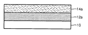
図1に示すように、下部膜10上に非晶質アルミニウム酸化物層12aを形成する。非晶質アルミニウム酸化物層12aは、例えばAl2O3層でありうる。非晶質アルミニウム酸化物層12aは、ALD(Atomic Layer Deposition)、スパッタリングまたはCVD(Chemical Vapor Deposition)法のような色々な蒸着方法で形成できる。非晶質アルミニウム酸化物層12a上に非晶質クロム酸化物層14aを形成する。非晶質クロム酸化物層14aは、例えばCr2O3層でありうる。非晶質クロム酸化物層14aは、非晶質アルミニウム酸化物層12aを形成する方法と同じ方法で形成できる。
次いで、非晶質クロム酸化物層14aを熱処理(以下、第1熱処理)して結晶化する。前記第1熱処理は、非晶質アルミニウム酸化物層12aの結晶化に影響を与えない温度で実施できる。例えば、前記第1熱処理は、600ないし900℃で実施できるが、非晶質アルミニウム酸化物層12aに影響を与えないために700℃以下で実施することが望ましい。前記第1熱処理により、非晶質クロム酸化物層14aは、図2に示したようにアルファ相の結晶構造を有するクロム酸化物層14となる。
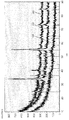
図8は、前記第1熱処理により形成された結晶質のクロム酸化物層14がアルファ相の結晶構造を有することを確認するために実施したX線回折分析実験の結果を示すグラフである。
図8において、第1グラフG1は、非晶質クロム酸化物層14aに対する結果である。そして、第2グラフG2は、非晶質クロム酸化物層14aを形成した後、600℃で熱処理した結果物に対するX線回折分析結果を表す。また、第3グラフG3は、非晶質クロム酸化物層14aを形成した後、700℃で熱処理した結果物に対するX線回折分析結果を表す。
第1グラフG1と第2及び第3グラフG2,G3とを比較すれば、第2及び第3グラフG2,G3に第1グラフG1で見られない色々なピークが表れることが見られる。かかるピークは、アルファ相の結晶構造を有するクロム酸化物層で発見されるところ、かかる結果から、非晶質クロム酸化物層14aを700℃以下の温度で熱処理して得た結晶質のクロム酸化物層14の結晶構造はアルファ相であるということが分かる。
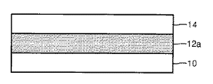
次いで、非晶質クロム酸化物層14aを熱処理してアルファ相の結晶構造を有するクロム酸化物層14を形成した後、非晶質アルミニウム酸化物層12aをアルファ相の結晶構造で結晶化するための熱処理(以下、第2熱処理)を実施する。このとき、アルファ相の結晶構造を有するクロム酸化物層14の存在によりナノサイズのアルファ相の核生成が誘発されるので、前記第2熱処理温度は、約1000℃であればよい。前記第2熱処理の結果、図3に示したようにアルファアルミニウム酸化物層12が形成される。次いで、アルファ相の結晶構造を有するクロム酸化物層14を除去する。クロム酸化物層14の厚さが薄い場合、除去しなくてもよい。
本発明者は、前記第2熱処理により形成された結晶質のアルミニウム酸化物層12がアルファ相の結晶構造を有することを確認するための実験を実施し、図9は、その結果を示す。
図9において、第1グラフG11は、非晶質クロム酸化物層14aなしに非晶質アルミニウム酸化物層12aのみを備える試片を1100℃で熱処理した結果物に対するX線回折分析結果を表す。第1グラフG11のピークP1は、非晶質クロム酸化物層14aのない状態で1100℃で熱処理されて形成された結晶質のアルミニウム酸化物層はガンマ相の結晶構造を有していることを表す。
図9において、第2グラフG22は、非晶質アルミニウム酸化物層12a上に非晶質クロム酸化物層14aを形成した後、その結果物を700℃で熱処理した後に測定したX線回折分析結果を表す。そして、第3グラフG33は、非晶質アルミニウム酸化物層12a上に非晶質クロム酸化物層14aを形成した後、非晶質クロム酸化物層14a及び非晶質アルミニウム酸化物層12aを結晶化するために、それぞれ700℃及び1050℃で熱処理した後に測定した結果を表す。また、第4グラフG44は、非晶質アルミニウム酸化物層12a上に非晶質クロム酸化物層14aを形成した後、その結果物を1050℃で熱処理した後に測定した結果を表す。
第1グラフG11と第2ないし第4グラフG22ないしG44とを比較すれば、第2ないし第4グラフG22ないしG44には、第1グラフG11に表れるピークP1が表れないことで、第2ないし第4グラフG22ないしG44に該当する試片の場合、ガンマ相の結晶構造を有するアルミニウム酸化物層の形成が抑制されることが分かる。
かかる結果は、非晶質アルミニウム酸化物層12a上にアルファ相の結晶構造を有するクロム酸化物層14が存在する場合、アルファ相のクロム酸化物層14からアルファ相の核生成が誘発され、これによって後続の熱処理により結晶化されるアルミニウム酸化物層の結晶構造は、ガンマ相でないアルファ相であることを表す。
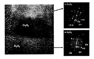
図10は、非晶質アルミニウム酸化物層上に非晶質クロム酸化物層を蒸着した後、その結果物を900℃で熱処理して結晶化したサンプルに対する透過電子顕微鏡(Transmission Electron Microscope:TEM)写真を示す。
図10に示すように、アルファ相の結晶構造を有するクロム酸化物層及びアルミニウム酸化物層が形成されたことが分かる。
図11は、ガンマ相の結晶構造を有するアルミニウム酸化物層に対するアルファ相の結晶構造を有するクロム酸化物層の影響を確認するために実施した実験の結果を表す。実験は、1100℃で熱処理した結晶質のアルミニウム酸化物層上に非晶質クロム酸化物層を蒸着した後、結晶化のためにその結果物を900℃で熱処理した。
図11に示すように、ピークP2の位置から見るとき、1100℃の熱処理により既にガンマ相に結晶化されたアルミニウム酸化物層の結晶構造は、アルファ相のクロム酸化物層を利用しても、アルファ相に変化せず、ガンマ相を維持することが分かる。
一方、前述した図1ないし図3に示したアルファアルミニウム酸化物層の形成方法が半導体素子の製造方法に適用される場合、例えば、電荷トラップ型メモリ素子の製造方法に適用される場合、前記アルファアルミニウム酸化物層の形成方法は、前記電荷トラップ型メモリ素子の製造方法においてブロッキング絶縁層の形成過程に適用される。
また、アルファ相の結晶構造を有するクロム酸化物層14の代わりに、アルファ相の核生成を誘発する他の物質層が使われるが、例えば、アルファFeO3層、Ga2O3層、Rh2O3層、Ti2O3層、V2O3層、ガンマAl2S3層、Co2As3層などが使われる。アルファ相の結晶構造を有するクロム酸化物層14及びそれらの代替物質層は、アルファアルミニウム酸化物層12を形成するとき、その結晶化温度を低める役割を行うところ、結晶化温度下降層または結晶化温度を低める結晶質補助層といえる。したがって、非晶質クロム酸化物層14aは、非晶質温度下降層または非晶質補助層といえる。
また、非晶質アルミニウム酸化物層12aは、非晶質クロム酸化物層14aの形成前や後に緻密化工程を実施できる。前記緻密化工程は、非晶質クロム酸化物層14aを形成する前に実施することがさらに望ましい。そして、前記緻密化工程は、非晶質アルミニウム酸化物層12aの結晶化に影響を与えないほどの温度、例えば800℃以下で実施できる。
本発明者は、アルファアルミニウム酸化物層12の形成に対する緻密化工程の影響を確認するための実験を実施した。この実験は、非晶質クロム酸化物層14aを形成する前に、非晶質アルミニウム酸化物層12aに対する緻密化工程を実施することを除いては、図9の結果を得るための実験と同一に進めた。そして、非晶質アルミニウム酸化物層の緻密化のための熱処理は、800℃で実施した。
図12は、前記緻密化工程の影響を確認するための実験の結果を表す。
図12において、第1グラフGG1は、非晶質クロム酸化物層14aなしに非晶質アルミニウム酸化物層12aのみを備える試片を1100℃で熱処理した結果物に対するX線回折分析結果を表す。第1グラフGG1のピークP11は、非晶質クロム酸化物層14aのない状態で1100℃で熱処理されて形成された結晶質のアルミニウム酸化物層はガンマ相の結晶構造を有していることを表す。
図12において、第2グラフGG2は、非晶質アルミニウム酸化物層12a上に非晶質クロム酸化物層14aを形成した後、その結果物を700℃で熱処理した後に測定したX線回折分析結果を表す。そして、第3グラフGG3は、非晶質アルミニウム酸化物層12a上に非晶質クロム酸化物層14aを形成した後、非晶質クロム酸化物層14a及び非晶質アルミニウム酸化物層12aを結晶化するために、それぞれ700℃及び1050℃で熱処理した後に測定した結果を表す。また、第4グラフGG4は、非晶質アルミニウム酸化物層12a上に非晶質クロム酸化物層14aを形成した後、その結果物を1050℃で熱処理した後に測定した結果を表す。
第1グラフGG1と第2ないし第4グラフGG2ないしGG4とを比較し、また、図9の第2ないし第4グラフG22ないしG44と図12の第2ないし第4グラフGG2ないしGG4とを比較すれば、図12の第2ないし第4グラフGG2ないしGG4は、結晶質のアルミニウム酸化物層にガンマ相の結晶構造とアルファ相の結晶構造とが混ざっていることが分かる。
次いで、図4ないし図7を参照して、本発明の実施形態による電荷トラップ型メモリ素子の製造方法を説明する。
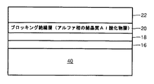
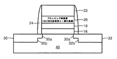
図4に示すように、基板40上にトンネリング膜16を形成する。基板40は、シリコン基板で形成できる。トンネリング膜16は、熱酸化方法で形成できる。トンネリング膜16上に電荷保存層18を形成する。電荷保存層18は、LPCVD(Low Pressure Chemical Vapor Deposition)法または他の積層方法で形成できる。電荷保存層18は、シリコン窒化物層、例えばSi3N4層、金属ナノドット及びシリコンナノドットのうちいずれか一つを含む。また、電荷保存層18は、シリコン窒化物層、金属ナノドット及びシリコンナノドットのうち少なくとも二つを含む複層または混合された構造で形成できる。また、電荷保存層18は、ドーピングされたポリシリコン膜、シリコン窒化膜、HfO2膜、La2O3膜及びZrO2膜のうちいずれか一つまたはそれらの混合物のうちいずれか一つでありうる。
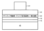
電荷保存層18を形成した後、その上にブロッキング絶縁層20を形成する。ブロッキング絶縁層20は、アルファアルミニウム酸化物層でありうる。このとき、ブロッキング絶縁層20は、前述した図1ないし図3で説明した方法で形成できる。かかるブロッキング絶縁層20上にゲート電極22を形成する。このとき、ブロッキング絶縁層20上に形成されたアルファ相の結晶質クロム酸化物層を除去した後、ゲート電極22を形成することが望ましいが、前記結晶質のクロム酸化物層の厚さが薄い場合、前記結晶質のクロム酸化物層上にゲート電極22を形成してもよい。ゲート電極22は、仕事関数が4.0eV以上でありうるが、例えばTaN電極でありうる。
図5に示すように、ゲート電極22上にマスクMを形成した後、マスクMの周囲のゲート電極22及びその下部の積層物20,18,16を順次にエッチングする。
図6は、前記エッチングの結果を表す。図6に示すように、前記エッチングによりトンネリング膜16、電荷保存層18、ブロッキング絶縁層20及びゲート電極22で構成されるゲート積層物GSが形成されたことが分かる。前記エッチングにより露出された基板40に導電性不純物を注入して、基板40に第1及び第2の浅い不純物領域30a,32aを形成する。次いで、マスクMを除去する。マスクMは、第1及び第2の浅い不純物領域30a,32aを形成する前に除去してもよい。
図7に示すように、ゲート積層物GSの側面にゲートスペーサ24を形成する。ゲートスペーサ24は、基板40上にゲート積層物GSを覆う原料物質膜を形成した後、前記原料物質膜を基板40が露出されるまで異方性エッチングして形成できる。ゲートスペーサ24の形成後、基板40に導電性不純物を注入して、第1及び第2の浅い不純物領域30a,32aにそれぞれ第1及び第2の深い不純物領域30b,32bを形成する。その結果、基板40にLDD(Lightly Doped Drain)構造の第1及び第2不純物領域30,32が形成される。第1及び第2不純物領域30,32のうち一つはソース領域、残りはドレイン領域である。
一方、後続工程でゲート積層物GSは層間絶縁層で覆われることに鑑みれば、ゲートスペーサ24の形成は選択的でありうる。ゲートスペーサ24の形成を省略する場合、第1及び第2不純物領域30,32は、第1及び第2の浅い不純物領域30a,32aと同じになる。
前記説明で多くの事項が具体的に記載されているが、それらは、発明の範囲を限定するというより、望ましい実施形態の例示として解釈されねばならない。例えば、当業者ならば、非晶質クロム酸化物層を結晶化して、アルファ相の結晶質クロム酸化物層を非晶質アルミニウム酸化物層上に形成する代わり、アルファ相の結晶質クロム酸化物層を非晶質アルミニウム酸化物層上に直接蒸着できるであろう。また、アルファ相の結晶質クロム酸化物層の代わりにアルファ核の生成が可能ならば、金属層を形成することもできるであろう。
本発明は、電荷トラップ型メモリ素子の製造に適用可能である。本発明によって製造された電荷トラップ型メモリ素子は、携帯用メモリスティックやデジタル家電製品、MP3、携帯電話、カムコーダ、GPS、コンピュータなど不揮発性メモリ素子が必要なあらゆる電子製品に適用可能である。
10 下部膜
12 アルファアルミニウム酸化物層
12a 非晶質アルミニウム酸化物層
14 結晶質のクロム酸化物層
14a 非晶質クロム酸化物層
16 トンネリング膜
18 電荷保存層
20 ブロッキング絶縁層
22 ゲート電極
24 ゲートスペーサ
30 第1不純物領域
30a 第1の浅い不純物領域
30b 第1の深い不純物領域
32 第2不純物領域
32a 第2の浅い不純物領域
32b 第2の深い不純物領域
40 基板
GS ゲート積層物
12 アルファアルミニウム酸化物層
12a 非晶質アルミニウム酸化物層
14 結晶質のクロム酸化物層
14a 非晶質クロム酸化物層
16 トンネリング膜
18 電荷保存層
20 ブロッキング絶縁層
22 ゲート電極
24 ゲートスペーサ
30 第1不純物領域
30a 第1の浅い不純物領域
30b 第1の深い不純物領域
32 第2不純物領域
32a 第2の浅い不純物領域
32b 第2の深い不純物領域
40 基板
GS ゲート積層物
Claims (19)
- 下部膜上に非晶質アルミニウム酸化物層を形成する第1ステップと、
前記非晶質アルミニウム酸化物層上に結晶質補助層を形成する第2ステップと、
前記非晶質アルミニウム酸化物層を結晶化する第3ステップと、を含むことを特徴とするアルファアルミニウム酸化物層の形成方法。 - 前記結晶質補助層を除去する第4ステップをさらに含むことを特徴とする請求項1に記載のアルファアルミニウム酸化物層の形成方法。
- 前記下部膜は、電荷保存物質で形成することを特徴とする請求項1に記載のアルファアルミニウム酸化物層の形成方法。
- 前記電荷保存物質は、シリコン窒化物であることを特徴とする請求項3に記載のアルファアルミニウム酸化物層の形成方法。
- 前記第2ステップは、
前記非晶質アルミニウム酸化物層上に非晶質補助層を形成するステップと、
前記非晶質補助層を結晶化するステップと、を含むことを特徴とする請求項1に記載のアルファアルミニウム酸化物層の形成方法。 - 前記結晶質補助層を形成する前に、前記非晶質アルミニウム酸化物層に対する緻密化工程を実施することを特徴とする請求項1に記載のアルファアルミニウム酸化物層の形成方法。
- 前記非晶質補助層を形成する前に、前記非晶質アルミニウム酸化物層に対する緻密化工程を実施することを特徴とする請求項5に記載のアルファアルミニウム酸化物層の形成方法。
- 前記非晶質補助層の結晶化及び前記非晶質アルミニウム酸化物層の結晶化は、1000℃より低い温度で同時に実施することを特徴とする請求項5に記載のアルファアルミニウム酸化物層の形成方法。
- 前記結晶質補助層は、アルファ相の結晶構造を有するCr2O3層、アルファFeO3層、Ga2O3層、Rh2O3層、Ti2O3層、V2O3層、ガンマAl2S3層及びCo2As3層のうちいずれか一つであることを特徴とする請求項1に記載のアルファアルミニウム酸化物層の形成方法。
- 前記非晶質補助層の結晶化は、前記非晶質アルミニウム酸化物層の結晶化温度より低い温度で実施することを特徴とする請求項5に記載のアルファアルミニウム酸化物層の形成方法。
- 前記非晶質補助層の結晶化は、800℃以下で実施することを特徴とする請求項10に記載のアルファアルミニウム酸化物層の形成方法。
- 前記第4ステップで、前記補助層の一部の厚さは残すことを特徴とする請求項2に記載のアルファアルミニウム酸化物層の形成方法。
- 前記結晶質補助層は、アルファ相の結晶構造を有するCr2O3層、アルファFeO3層、Ga2O3層、Rh2O3層、Ti2O3層、V2O3層、ガンマAl2S3層及びCo2As3層のうちいずれか一つであることを特徴とする請求項5に記載のアルファアルミニウム酸化物層の形成方法。
- トンネリング膜、電荷保存層、ブロッキング絶縁層及びゲート電極を備える電荷トラップ型メモリ素子の製造方法において、
前記ブロッキング絶縁層は、
アルファ相の結晶構造を有するアルミニウム酸化物層であって、前記電荷保存層を下部膜として使用して請求項1に記載の方法で形成することを特徴とする電荷トラップ型メモリ素子の製造方法。 - 前記電荷保存層は、シリコン窒化膜、金属ナノドット及びシリコンナノドットのうちいずれか一つを含むことを特徴とする請求項14に記載の電荷トラップ型メモリ素子の製造方法。
- 前記電荷保存層は、シリコン窒化膜、金属ナノドット及びシリコンナノドットのうち少なくとも二つを含む複層または混合された構造で形成されたことを特徴とする請求項14に記載の電荷トラップ型メモリ素子の製造方法。
- 前記電荷保存層は、ドーピングされたポリシリコン膜、シリコン窒化膜、HfO2膜、La2O3膜及びZrO2膜のうちいずれか一つまたはそれらの混合物のうちいずれか一つであることを特徴とする請求項14に記載の電荷トラップ型メモリ素子の製造方法。
- 前記ゲート電極は、仕事関数が4.0eV以上であることを特徴とする請求項14に記載の電荷トラップ型メモリ素子の製造方法。
- 前記ゲート電極は、TaN電極であることを特徴とする請求項18に記載の電荷トラップ型メモリ素子の製造方法。
Applications Claiming Priority (1)
| Application Number | Priority Date | Filing Date | Title |
|---|---|---|---|
| KR1020070087290A KR101281682B1 (ko) | 2007-08-29 | 2007-08-29 | 알루미늄 산화물층 형성방법 및 이를 이용한 전하 트랩형메모리 소자의 제조 방법 |
Publications (1)
| Publication Number | Publication Date |
|---|---|
| JP2009060102A true JP2009060102A (ja) | 2009-03-19 |
Family
ID=40408141
Family Applications (1)
| Application Number | Title | Priority Date | Filing Date |
|---|---|---|---|
| JP2008215719A Pending JP2009060102A (ja) | 2007-08-29 | 2008-08-25 | アルミニウム酸化物層の形成方法及びそれを利用した電荷トラップ型メモリ素子の製造方法 |
Country Status (4)
| Country | Link |
|---|---|
| US (1) | US8043952B2 (ja) |
| JP (1) | JP2009060102A (ja) |
| KR (1) | KR101281682B1 (ja) |
| CN (1) | CN101378013A (ja) |
Cited By (5)
| Publication number | Priority date | Publication date | Assignee | Title |
|---|---|---|---|---|
| JP2018154552A (ja) * | 2014-09-12 | 2018-10-04 | ホンコン バプテスト ユニバーシティ | サファイア薄膜コーティングされたフレキシブル基板 |
| US10941480B2 (en) | 2011-12-23 | 2021-03-09 | Hkbu R&D Licensing Limited | Sapphire thin film coated flexible substrate |
| US11028471B2 (en) | 2011-12-23 | 2021-06-08 | Hkbu R&D Licensing Limited | Sapphire thin film coated substrate |
| US11535926B2 (en) | 2011-12-23 | 2022-12-27 | Hkbu R&D Licensing Limited | Sapphire thin film coated substrate |
| US11713503B2 (en) | 2011-12-23 | 2023-08-01 | Hong Kong Baptist University | Sapphire coated substrate with a flexible, anti-scratch and multi-layer coating |
Families Citing this family (15)
| Publication number | Priority date | Publication date | Assignee | Title |
|---|---|---|---|---|
| JP5245287B2 (ja) | 2007-05-18 | 2013-07-24 | ソニー株式会社 | 半導体装置の製造方法、薄膜トランジスタ基板の製造方法および表示装置の製造方法 |
| US10446681B2 (en) | 2017-07-10 | 2019-10-15 | Micron Technology, Inc. | NAND memory arrays, and devices comprising semiconductor channel material and nitrogen |
| US10276411B2 (en) | 2017-08-18 | 2019-04-30 | Applied Materials, Inc. | High pressure and high temperature anneal chamber |
| US10559466B2 (en) | 2017-12-27 | 2020-02-11 | Micron Technology, Inc. | Methods of forming a channel region of a transistor and methods used in forming a memory array |
| US10297611B1 (en) | 2017-12-27 | 2019-05-21 | Micron Technology, Inc. | Transistors and arrays of elevationally-extending strings of memory cells |
| EP3768874A4 (en) | 2018-03-19 | 2022-03-30 | Applied Materials, Inc. | METHODS FOR DEPOSITING COATINGS ON AEROSPACE ELEMENTS |
| EP3784815A4 (en) | 2018-04-27 | 2021-11-03 | Applied Materials, Inc. | PROTECTION OF COMPONENTS AGAINST CORROSION |
| US11009339B2 (en) | 2018-08-23 | 2021-05-18 | Applied Materials, Inc. | Measurement of thickness of thermal barrier coatings using 3D imaging and surface subtraction methods for objects with complex geometries |
| WO2020219332A1 (en) | 2019-04-26 | 2020-10-29 | Applied Materials, Inc. | Methods of protecting aerospace components against corrosion and oxidation |
| US11794382B2 (en) | 2019-05-16 | 2023-10-24 | Applied Materials, Inc. | Methods for depositing anti-coking protective coatings on aerospace components |
| US11697879B2 (en) | 2019-06-14 | 2023-07-11 | Applied Materials, Inc. | Methods for depositing sacrificial coatings on aerospace components |
| US11466364B2 (en) * | 2019-09-06 | 2022-10-11 | Applied Materials, Inc. | Methods for forming protective coatings containing crystallized aluminum oxide |
| US11519066B2 (en) | 2020-05-21 | 2022-12-06 | Applied Materials, Inc. | Nitride protective coatings on aerospace components and methods for making the same |
| EP4175772A1 (en) | 2020-07-03 | 2023-05-10 | Applied Materials, Inc. | Methods for refurbishing aerospace components |
| US11538919B2 (en) | 2021-02-23 | 2022-12-27 | Micron Technology, Inc. | Transistors and arrays of elevationally-extending strings of memory cells |
Family Cites Families (7)
| Publication number | Priority date | Publication date | Assignee | Title |
|---|---|---|---|---|
| KR100371142B1 (ko) * | 1998-12-30 | 2003-03-31 | 주식회사 하이닉스반도체 | 반도체소자의캐패시터형성방법 |
| KR20030002035A (ko) * | 2001-06-30 | 2003-01-08 | 주식회사 하이닉스반도체 | 원자층증착법에 의한 박막의 형성 방법 및 그를 이용한캐패시터의 제조 방법 |
| US7122415B2 (en) * | 2002-09-12 | 2006-10-17 | Promos Technologies, Inc. | Atomic layer deposition of interpoly oxides in a non-volatile memory device |
| JP4619637B2 (ja) * | 2003-09-09 | 2011-01-26 | 財団法人国際科学振興財団 | 半導体装置及びその製造方法 |
| KR100580771B1 (ko) * | 2004-10-01 | 2006-05-15 | 주식회사 하이닉스반도체 | 플래쉬 메모리소자의 형성방법 |
| KR100772109B1 (ko) * | 2006-06-30 | 2007-11-01 | 주식회사 하이닉스반도체 | 반도체 소자의 소자분리막 형성방법 |
| TWI316746B (en) * | 2006-10-03 | 2009-11-01 | Macronix Int Co Ltd | Non-volatile memory and method of manufacturing the same |
-
2007
- 2007-08-29 KR KR1020070087290A patent/KR101281682B1/ko active IP Right Grant
-
2008
- 2008-05-22 US US12/153,655 patent/US8043952B2/en active Active
- 2008-07-29 CN CNA2008101280729A patent/CN101378013A/zh active Pending
- 2008-08-25 JP JP2008215719A patent/JP2009060102A/ja active Pending
Cited By (5)
| Publication number | Priority date | Publication date | Assignee | Title |
|---|---|---|---|---|
| US10941480B2 (en) | 2011-12-23 | 2021-03-09 | Hkbu R&D Licensing Limited | Sapphire thin film coated flexible substrate |
| US11028471B2 (en) | 2011-12-23 | 2021-06-08 | Hkbu R&D Licensing Limited | Sapphire thin film coated substrate |
| US11535926B2 (en) | 2011-12-23 | 2022-12-27 | Hkbu R&D Licensing Limited | Sapphire thin film coated substrate |
| US11713503B2 (en) | 2011-12-23 | 2023-08-01 | Hong Kong Baptist University | Sapphire coated substrate with a flexible, anti-scratch and multi-layer coating |
| JP2018154552A (ja) * | 2014-09-12 | 2018-10-04 | ホンコン バプテスト ユニバーシティ | サファイア薄膜コーティングされたフレキシブル基板 |
Also Published As
| Publication number | Publication date |
|---|---|
| US8043952B2 (en) | 2011-10-25 |
| KR20090022170A (ko) | 2009-03-04 |
| CN101378013A (zh) | 2009-03-04 |
| KR101281682B1 (ko) | 2013-07-03 |
| US20090061613A1 (en) | 2009-03-05 |
Similar Documents
| Publication | Publication Date | Title |
|---|---|---|
| JP2009060102A (ja) | アルミニウム酸化物層の形成方法及びそれを利用した電荷トラップ型メモリ素子の製造方法 | |
| JP4552973B2 (ja) | 半導体装置の製造方法 | |
| JP4792132B2 (ja) | 誘電体ならびに半導体装置の製造方法、プログラム、および、記録媒体 | |
| JP4465413B1 (ja) | 誘電体膜、誘電体膜の製造方法、半導体装置、および、記録媒体 | |
| TWI609480B (zh) | Non-volatile semiconductor memory and non-volatile semiconductor memory manufacturing method | |
| US11515419B2 (en) | Ferroelectric semiconductor device and method of manufacturing the same | |
| JP2020155644A (ja) | 半導体記憶装置 | |
| JP2005005715A (ja) | Sonosメモリ素子およびその製造方法 | |
| JP2006203200A (ja) | 高誘電率の絶縁膜を含む半導体素子及びその製造方法 | |
| US20080169501A1 (en) | Flash memory device with hybrid structure charge trap layer and method of manufacturing same | |
| JP2015053474A (ja) | 半導体装置およびその製造方法 | |
| CN106783867B (zh) | 存储器电荷存储结构中的吸气剂 | |
| TWI776983B (zh) | 半導體裝置及其製造方法 | |
| JP7357901B2 (ja) | トランジスタおよび不揮発性メモリ | |
| JP2009055030A (ja) | 結晶質アルミニウム酸化物層のエネルギーバンドギャップを高める方法及びエネルギーバンドギャップの高い結晶質アルミニウム酸化物層を備える電荷トラップメモリ素子の製造方法 | |
| JP2008227492A (ja) | 電荷トラップ型メモリ素子 | |
| JP2002261175A (ja) | 不揮発性半導体記憶装置およびその製造方法 | |
| JP4177803B2 (ja) | 半導体装置の製造方法 | |
| JP2009049409A (ja) | 不揮発性メモリ素子及びその製造方法 | |
| TWI316746B (en) | Non-volatile memory and method of manufacturing the same | |
| TWI822805B (zh) | 半導體元件及其製造方法 | |
| JP2009049418A (ja) | 電荷トラップ層を有する不揮発性メモリ素子及びその製造方法 | |
| KR101065060B1 (ko) | 전하 트랩형 비휘발성 메모리 | |
| JP2006222434A (ja) | シリコンリッチ酸化ケイ素膜を備えるメモリ素子の構造及びその製造方法 | |
| TWI395298B (zh) | 非揮發性記憶體及其製造方法 |