JP2008517465A - 半導体組立てと試験設備用のダイ・レベル追跡遂行機構 - Google Patents
半導体組立てと試験設備用のダイ・レベル追跡遂行機構 Download PDFInfo
- Publication number
- JP2008517465A JP2008517465A JP2007536813A JP2007536813A JP2008517465A JP 2008517465 A JP2008517465 A JP 2008517465A JP 2007536813 A JP2007536813 A JP 2007536813A JP 2007536813 A JP2007536813 A JP 2007536813A JP 2008517465 A JP2008517465 A JP 2008517465A
- Authority
- JP
- Japan
- Prior art keywords
- die
- string
- source object
- strings
- units
- Prior art date
- Legal status (The legal status is an assumption and is not a legal conclusion. Google has not performed a legal analysis and makes no representation as to the accuracy of the status listed.)
- Withdrawn
Links
Images


Classifications
-
- G—PHYSICS
- G06—COMPUTING OR CALCULATING; COUNTING
- G06Q—INFORMATION AND COMMUNICATION TECHNOLOGY [ICT] SPECIALLY ADAPTED FOR ADMINISTRATIVE, COMMERCIAL, FINANCIAL, MANAGERIAL OR SUPERVISORY PURPOSES; SYSTEMS OR METHODS SPECIALLY ADAPTED FOR ADMINISTRATIVE, COMMERCIAL, FINANCIAL, MANAGERIAL OR SUPERVISORY PURPOSES, NOT OTHERWISE PROVIDED FOR
- G06Q10/00—Administration; Management
- G06Q10/06—Resources, workflows, human or project management; Enterprise or organisation planning; Enterprise or organisation modelling
-
- H—ELECTRICITY
- H01—ELECTRIC ELEMENTS
- H01L—SEMICONDUCTOR DEVICES NOT COVERED BY CLASS H10
- H01L21/00—Processes or apparatus adapted for the manufacture or treatment of semiconductor or solid state devices or of parts thereof
- H01L21/02—Manufacture or treatment of semiconductor devices or of parts thereof
- H01L21/04—Manufacture or treatment of semiconductor devices or of parts thereof the devices having potential barriers, e.g. a PN junction, depletion layer or carrier concentration layer
- H01L21/18—Manufacture or treatment of semiconductor devices or of parts thereof the devices having potential barriers, e.g. a PN junction, depletion layer or carrier concentration layer the devices having semiconductor bodies comprising elements of Group IV of the Periodic Table or AIIIBV compounds with or without impurities, e.g. doping materials
- H01L21/30—Treatment of semiconductor bodies using processes or apparatus not provided for in groups H01L21/20 - H01L21/26
- H01L21/302—Treatment of semiconductor bodies using processes or apparatus not provided for in groups H01L21/20 - H01L21/26 to change their surface-physical characteristics or shape, e.g. etching, polishing, cutting
- H01L21/304—Mechanical treatment, e.g. grinding, polishing, cutting
-
- G—PHYSICS
- G06—COMPUTING OR CALCULATING; COUNTING
- G06Q—INFORMATION AND COMMUNICATION TECHNOLOGY [ICT] SPECIALLY ADAPTED FOR ADMINISTRATIVE, COMMERCIAL, FINANCIAL, MANAGERIAL OR SUPERVISORY PURPOSES; SYSTEMS OR METHODS SPECIALLY ADAPTED FOR ADMINISTRATIVE, COMMERCIAL, FINANCIAL, MANAGERIAL OR SUPERVISORY PURPOSES, NOT OTHERWISE PROVIDED FOR
- G06Q10/00—Administration; Management
- G06Q10/08—Logistics, e.g. warehousing, loading or distribution; Inventory or stock management
-
- H—ELECTRICITY
- H01—ELECTRIC ELEMENTS
- H01L—SEMICONDUCTOR DEVICES NOT COVERED BY CLASS H10
- H01L21/00—Processes or apparatus adapted for the manufacture or treatment of semiconductor or solid state devices or of parts thereof
Landscapes
- Engineering & Computer Science (AREA)
- Business, Economics & Management (AREA)
- Economics (AREA)
- Physics & Mathematics (AREA)
- General Physics & Mathematics (AREA)
- Strategic Management (AREA)
- Human Resources & Organizations (AREA)
- Entrepreneurship & Innovation (AREA)
- General Business, Economics & Management (AREA)
- Quality & Reliability (AREA)
- Theoretical Computer Science (AREA)
- Tourism & Hospitality (AREA)
- Development Economics (AREA)
- Marketing (AREA)
- Operations Research (AREA)
- Computer Hardware Design (AREA)
- Manufacturing & Machinery (AREA)
- Microelectronics & Electronic Packaging (AREA)
- Condensed Matter Physics & Semiconductors (AREA)
- Power Engineering (AREA)
- Educational Administration (AREA)
- Game Theory and Decision Science (AREA)
- General Factory Administration (AREA)
- Testing Or Measuring Of Semiconductors Or The Like (AREA)
Applications Claiming Priority (2)
| Application Number | Priority Date | Filing Date | Title |
|---|---|---|---|
| US61880504P | 2004-10-15 | 2004-10-15 | |
| PCT/US2005/036548 WO2006044399A1 (en) | 2004-10-15 | 2005-10-12 | Die-level traceability mechanism for semiconductor assembly and test facility |
Publications (2)
| Publication Number | Publication Date |
|---|---|
| JP2008517465A true JP2008517465A (ja) | 2008-05-22 |
| JP2008517465A5 JP2008517465A5 (enExample) | 2008-11-27 |
Family
ID=35754092
Family Applications (1)
| Application Number | Title | Priority Date | Filing Date |
|---|---|---|---|
| JP2007536813A Withdrawn JP2008517465A (ja) | 2004-10-15 | 2005-10-12 | 半導体組立てと試験設備用のダイ・レベル追跡遂行機構 |
Country Status (7)
| Country | Link |
|---|---|
| US (2) | US7343214B2 (enExample) |
| EP (1) | EP1810326A1 (enExample) |
| JP (1) | JP2008517465A (enExample) |
| KR (1) | KR20070085369A (enExample) |
| CN (1) | CN101040290A (enExample) |
| TW (1) | TW200629026A (enExample) |
| WO (1) | WO2006044399A1 (enExample) |
Families Citing this family (9)
| Publication number | Priority date | Publication date | Assignee | Title |
|---|---|---|---|---|
| GB0800227D0 (en) * | 2008-01-07 | 2008-02-13 | Metryx Ltd | Method of controlling semiconductor device fabrication |
| TWI442401B (zh) * | 2009-12-30 | 2014-06-21 | Macronix Int Co Ltd | 共享輸入封裝之三維晶片選取 |
| CN102640253B (zh) | 2010-10-04 | 2014-06-18 | 晟碟半导体(上海)有限公司 | 分立组件后向可追溯性和半导体装置前向可追溯性 |
| US9559113B2 (en) | 2014-05-01 | 2017-01-31 | Macronix International Co., Ltd. | SSL/GSL gate oxide in 3D vertical channel NAND |
| KR20160018227A (ko) * | 2014-08-08 | 2016-02-17 | 에스케이하이닉스 주식회사 | 웨이퍼 처리 시스템 및 이를 이용한 웨이퍼 처리 방법 |
| US10419410B2 (en) * | 2016-12-15 | 2019-09-17 | Seagate Technology Llc | Automatic generation of unique identifiers for distributed directory management users |
| KR102653937B1 (ko) | 2018-07-17 | 2024-04-02 | 삼성전자주식회사 | 반도체 장치의 테스트 방법및 반도체 장치의 테스트 시스템 |
| US11063000B2 (en) * | 2019-01-29 | 2021-07-13 | Infineon Technologies Ag | Semiconductor package authentication feature |
| US11450616B2 (en) | 2020-07-29 | 2022-09-20 | Nxp Usa, Inc. | Using a backside mask layer for forming a unique die mark identifier pattern |
Family Cites Families (83)
| Publication number | Priority date | Publication date | Assignee | Title |
|---|---|---|---|---|
| US103628A (en) * | 1870-05-31 | Lemuel w | ||
| US21265A (en) * | 1858-08-24 | Improvement in rotary harrows | ||
| US225385A (en) * | 1880-03-09 | Service-pipe box | ||
| US4767A (en) * | 1846-09-19 | Pike-engine | ||
| US132060A (en) * | 1872-10-08 | Improvement in windmills | ||
| US6404A (en) * | 1849-05-01 | shaw and ezra gould | ||
| US744A (en) * | 1838-05-17 | Mode of cutting off steam in steam-engines | ||
| US158795A (en) * | 1875-01-19 | Improvement in clover-harvesters | ||
| US95172A (en) * | 1869-09-21 | Improved shoemakers tool | ||
| US5090A (en) * | 1847-05-01 | Improvement in diffusers for water-wheels | ||
| US26949A (en) * | 1860-01-24 | William lewis | ||
| US42780A (en) * | 1864-05-17 | Improvement in wood-splitting machines | ||
| US17708A (en) * | 1857-06-30 | Coloring yarn ijst the bobbin | ||
| US251472A (en) * | 1881-12-27 | sohmetzer | ||
| US106931A (en) * | 1870-08-30 | Improvement in machine for rounding fellies for wheels | ||
| US110270A (en) * | 1870-12-20 | Improvement in machines for making cigars | ||
| US187737A (en) * | 1877-02-27 | Improvement in mowing-machines | ||
| US183884A (en) * | 1876-10-31 | Improvement in gas-carbureters | ||
| US81756A (en) * | 1868-09-01 | Improved traveling-trunk | ||
| US62609A (en) * | 1867-03-05 | Improved life-pbeservdfg beeth | ||
| US38779A (en) * | 1863-06-02 | Improvement in thrashing-machines | ||
| US34785A (en) * | 1862-03-25 | Improvement in heaters | ||
| US76897A (en) * | 1868-04-21 | Improved composition foe blacking leatheb | ||
| US87113A (en) * | 1869-02-23 | Improvement in reel and swift | ||
| US224540A (en) * | 1880-02-17 | Caleb h | ||
| US176872A (en) * | 1876-05-02 | Improvement in gang-planks | ||
| US124437A (en) * | 1872-03-12 | Improvement in type writing-machines | ||
| US36677A (en) * | 1862-10-14 | Improvement in hoop-skirts | ||
| US157762A (en) * | 1874-12-15 | Improvement in bird-cages | ||
| US203591A (en) * | 1878-05-14 | Improvement in tools for trimming and finishing the edges of dash-boards | ||
| US256463A (en) * | 1882-04-18 | Journal-bearing | ||
| US141605A (en) * | 1873-08-05 | Improvement in packages for fruit | ||
| US5129974A (en) * | 1990-08-23 | 1992-07-14 | Colorcode Unlimited Corporation | Microlabelling system and method of making thin labels |
| JPH07123101B2 (ja) * | 1990-09-14 | 1995-12-25 | 株式会社東芝 | 半導体装置 |
| US5625816A (en) * | 1994-04-05 | 1997-04-29 | Advanced Micro Devices, Inc. | Method and system for generating product performance history |
| US6941556B1 (en) * | 1995-03-24 | 2005-09-06 | Sun Microsystems, Inc. | Method and system for type identification for multiple object interfaces in a distributed object environment |
| US5726920A (en) * | 1995-09-29 | 1998-03-10 | Advanced Micro Devices, Inc. | Watchdog system having data differentiating means for use in monitoring of semiconductor wafer testing line |
| US5751581A (en) * | 1995-11-13 | 1998-05-12 | Advanced Micro Devices | Material movement server |
| US5838361A (en) | 1996-01-11 | 1998-11-17 | Micron Technology, Inc. | Laser marking techniques |
| DE19640425A1 (de) | 1996-09-30 | 1998-04-02 | Siemens Ag | Verfahren zur Waferidentifizierung in der Chipfertigung und Vorrichtung zur Durchführung des Verfahrens |
| US6259960B1 (en) * | 1996-11-01 | 2001-07-10 | Joel Ltd. | Part-inspecting system |
| US6100486A (en) | 1998-08-13 | 2000-08-08 | Micron Technology, Inc. | Method for sorting integrated circuit devices |
| US6065113A (en) * | 1997-03-07 | 2000-05-16 | Texas Instruments Incorporated | Circuits, systems, and methods for uniquely identifying a microprocessor at the instruction set level employing one-time programmable register |
| US5856923A (en) | 1997-03-24 | 1999-01-05 | Micron Technology, Inc. | Method for continuous, non lot-based integrated circuit manufacturing |
| JPH1126333A (ja) * | 1997-06-27 | 1999-01-29 | Oki Electric Ind Co Ltd | 半導体装置及びその情報管理システム |
| US6446017B1 (en) * | 1997-08-21 | 2002-09-03 | Micron Technology, Inc. | Method and system for tracking manufacturing data for integrated circuit parts |
| JP3394895B2 (ja) | 1997-09-08 | 2003-04-07 | 沖電気工業株式会社 | 半導体記憶装置およびその製造方法 |
| US6128588A (en) * | 1997-10-01 | 2000-10-03 | Sony Corporation | Integrated wafer fab time standard (machine tact) database |
| US6216055B1 (en) * | 1997-12-16 | 2001-04-10 | Texas Instruments Incorporated | Partial semiconductor wafer processing |
| KR19990065486A (ko) * | 1998-01-14 | 1999-08-05 | 윤종용 | 반도체 제조설비 관리시스템의 공정조건 관리방법 |
| US6049624A (en) * | 1998-02-20 | 2000-04-11 | Micron Technology, Inc. | Non-lot based method for assembling integrated circuit devices |
| US6268641B1 (en) | 1998-03-30 | 2001-07-31 | Kabushiki Kaisha Toshiba | Semiconductor wafer having identification indication and method of manufacturing the same |
| WO2000014790A1 (en) * | 1998-09-03 | 2000-03-16 | Hitachi, Ltd. | Inspection system and method for producing electronic device by using the same |
| JP4951811B2 (ja) | 1999-03-24 | 2012-06-13 | 富士通セミコンダクター株式会社 | 半導体装置の製造方法 |
| US6337122B1 (en) | 2000-01-11 | 2002-01-08 | Micron Technology, Inc. | Stereolithographically marked semiconductors devices and methods |
| JP3555859B2 (ja) | 2000-03-27 | 2004-08-18 | 広島日本電気株式会社 | 半導体生産システム及び半導体装置の生産方法 |
| US6792563B1 (en) * | 2000-04-28 | 2004-09-14 | Intel Corporation | Method and apparatus for bus activity tracking |
| US6673692B2 (en) | 2000-06-28 | 2004-01-06 | Micron Technology, Inc. | Method and apparatus for marking microelectronic dies and microelectronic devices |
| JP3578057B2 (ja) | 2000-07-06 | 2004-10-20 | 株式会社日立製作所 | Id管理システム |
| US6568593B2 (en) * | 2000-07-14 | 2003-05-27 | Trumpf Gmbh + Co. | System and method for identification of tools and parts of tools for a fabricating machine |
| US6351684B1 (en) * | 2000-09-19 | 2002-02-26 | Advanced Micro Devices, Inc. | Mask identification database server |
| JP2002184872A (ja) | 2000-12-15 | 2002-06-28 | Hitachi Ltd | 認識番号を有する半導体装置、その製造方法及び電子装置 |
| JP2002190509A (ja) | 2000-12-22 | 2002-07-05 | Mitsubishi Electric Corp | 検査解析方法及び半導体装置 |
| US7031791B1 (en) * | 2001-02-27 | 2006-04-18 | Cypress Semiconductor Corp. | Method and system for a reject management protocol within a back-end integrated circuit manufacturing process |
| TW594590B (en) * | 2001-03-16 | 2004-06-21 | Taiwan Semiconductor Mfg | Split lot ID encoding system and method |
| US7100826B1 (en) * | 2001-03-26 | 2006-09-05 | Advanced Micro Devices, Inc. | Barcode marking of wafer products for inventory control |
| US6792365B2 (en) * | 2001-08-10 | 2004-09-14 | Micron Technology, Inc. | Sequential unique marking |
| US6555400B2 (en) * | 2001-08-22 | 2003-04-29 | Micron Technology, Inc. | Method for substrate mapping |
| JP2003115424A (ja) | 2001-10-03 | 2003-04-18 | Nec Corp | 半導体装置およびその識別方法、並びに半導体装置の製造装置 |
| EP1391853A1 (fr) | 2001-11-30 | 2004-02-25 | STMicroelectronics S.A. | Diversification d'un identifiant unique d'un circuit intégré |
| US6616034B2 (en) * | 2001-12-10 | 2003-09-09 | Fortrend Taiwan Scientific Corporation | Radio frequency identification device |
| US7035877B2 (en) | 2001-12-28 | 2006-04-25 | Kimberly-Clark Worldwide, Inc. | Quality management and intelligent manufacturing with labels and smart tags in event-based product manufacturing |
| US20030141605A1 (en) | 2002-01-25 | 2003-07-31 | Silicon Integrated Systems Corp. | Method of forming identifying mark on semiconductor wafer |
| JP4256115B2 (ja) | 2002-05-28 | 2009-04-22 | 富士通マイクロエレクトロニクス株式会社 | マーク認識方法及び半導体装置の製造方法 |
| US6952623B2 (en) | 2002-07-02 | 2005-10-04 | Texas Instruments, Inc. | Permanent chip ID using FeRAM |
| US20040034785A1 (en) | 2002-08-15 | 2004-02-19 | Horng-Ming Tai | Hardware and firmware encryption mechanism using unique chip die identification |
| US6974761B2 (en) | 2002-09-27 | 2005-12-13 | Oki Electric Industry Co. | Method of forming a semiconductor laser chip having a marker |
| US6839601B1 (en) | 2002-11-26 | 2005-01-04 | Advanced Micro Devices, Inc. | Fabrication architecture including enterprise resource planning integration |
| US6812477B2 (en) | 2002-12-04 | 2004-11-02 | Texas Instruments Incorporated | Integrated circuit identification |
| US7015795B2 (en) | 2002-12-30 | 2006-03-21 | Potomac Photonics, Inc. | Self-identifying integrated circuits and method for fabrication thereof |
| US6959229B2 (en) | 2003-03-07 | 2005-10-25 | Sdi Industries, Inc. | RFID control system |
| US20040251472A1 (en) | 2003-06-11 | 2004-12-16 | Broadcom Corporation | Memory cell for modification of revision identifier in an integrated circuit chip |
| US7415317B2 (en) | 2004-02-25 | 2008-08-19 | Micron Technology, Inc. | Method and system for correlating and combining production and non-production data for analysis |
-
2005
- 2005-10-12 WO PCT/US2005/036548 patent/WO2006044399A1/en not_active Ceased
- 2005-10-12 CN CNA2005800352387A patent/CN101040290A/zh active Pending
- 2005-10-12 EP EP05804118A patent/EP1810326A1/en not_active Withdrawn
- 2005-10-12 KR KR1020077011038A patent/KR20070085369A/ko not_active Withdrawn
- 2005-10-12 US US11/247,196 patent/US7343214B2/en not_active Expired - Fee Related
- 2005-10-12 JP JP2007536813A patent/JP2008517465A/ja not_active Withdrawn
- 2005-10-14 TW TW094136036A patent/TW200629026A/zh unknown
-
2007
- 2007-10-31 US US11/982,163 patent/US20080071413A1/en not_active Abandoned
Also Published As
| Publication number | Publication date |
|---|---|
| TW200629026A (en) | 2006-08-16 |
| US20080071413A1 (en) | 2008-03-20 |
| US20060085089A1 (en) | 2006-04-20 |
| CN101040290A (zh) | 2007-09-19 |
| US7343214B2 (en) | 2008-03-11 |
| WO2006044399A1 (en) | 2006-04-27 |
| KR20070085369A (ko) | 2007-08-27 |
| EP1810326A1 (en) | 2007-07-25 |
Similar Documents
| Publication | Publication Date | Title |
|---|---|---|
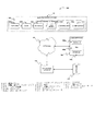
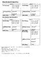
| US20080071413A1 (en) | Die-level traceability mechanism for semiconductor assembly and test facility | |
| US11853389B2 (en) | Methods and apparatus for sorting data | |
| US8881246B2 (en) | System and method for providing secured integrated engineering analysis | |
| EP1732016B1 (en) | Information processing apparatus, information processing method, and information processing program | |
| US6756796B2 (en) | Method of search and identify reference die | |
| US5448488A (en) | Computer-controlled individual chip management system for processing wafers | |
| JP2003324043A (ja) | レシピ配布管理データベースを備えた半導体ウェハ製造実行システム | |
| EP3432165A1 (en) | Database search system and method | |
| US8015040B2 (en) | Methods, systems, and computer program products for product randomization and analysis in a manufacturing environment | |
| US8825190B2 (en) | Priority calculation device, program, priority calculation system, and priority calculation method | |
| US7035705B2 (en) | System and method for process contamination prevention for semiconductor manufacturing | |
| US6929962B1 (en) | System and method for wafer acceptance test configuration | |
| TW542989B (en) | System and method to reduce bond program errors of integrated circuit bonders | |
| JP2008517465A5 (enExample) | ||
| US20040158344A1 (en) | Mask management device in semiconductor wafer production process | |
| US6694210B1 (en) | Process recipe modification in an integrated circuit fabrication apparatus | |
| CN111724143A (zh) | 基于rpa的流程元素定位方法及装置、计算设备、存储介质 | |
| US6909934B1 (en) | Efficient method of dynamic formulation of chamber selections for multiple chamber tools | |
| US20030220706A1 (en) | Wafer map host system | |
| CN101751402B (zh) | 地图信息管理方法及系统 | |
| US7433750B2 (en) | Data tracking method and system applied in semiconductor manufacturing | |
| JP2005071371A (ja) | コンピュータ支援設計ツールにおける設計要素を解析するシステムおよび方法 | |
| US6789235B1 (en) | Bond program verification system | |
| JP7055911B1 (ja) | 工事情報表示装置、工事情報表示方法及び工事情報表示プログラム | |
| US20160070250A1 (en) | Production management apparatus, production management method and recording medium |
Legal Events
| Date | Code | Title | Description |
|---|---|---|---|
| A521 | Request for written amendment filed |
Free format text: JAPANESE INTERMEDIATE CODE: A523 Effective date: 20081010 |
|
| A621 | Written request for application examination |
Free format text: JAPANESE INTERMEDIATE CODE: A621 Effective date: 20081010 |
|
| A761 | Written withdrawal of application |
Free format text: JAPANESE INTERMEDIATE CODE: A761 Effective date: 20100426 |