JP2008282902A - 配線基板及びその製造方法 - Google Patents
配線基板及びその製造方法 Download PDFInfo
- Publication number
- JP2008282902A JP2008282902A JP2007124276A JP2007124276A JP2008282902A JP 2008282902 A JP2008282902 A JP 2008282902A JP 2007124276 A JP2007124276 A JP 2007124276A JP 2007124276 A JP2007124276 A JP 2007124276A JP 2008282902 A JP2008282902 A JP 2008282902A
- Authority
- JP
- Japan
- Prior art keywords
- wiring board
- wiring
- hole
- electronic component
- plating layer
- Prior art date
- Legal status (The legal status is an assumption and is not a legal conclusion. Google has not performed a legal analysis and makes no representation as to the accuracy of the status listed.)
- Granted
Links
Images
Classifications
-
- H—ELECTRICITY
- H10—SEMICONDUCTOR DEVICES; ELECTRIC SOLID-STATE DEVICES NOT OTHERWISE PROVIDED FOR
- H10W—GENERIC PACKAGES, INTERCONNECTIONS, CONNECTORS OR OTHER CONSTRUCTIONAL DETAILS OF DEVICES COVERED BY CLASS H10
- H10W90/00—Package configurations
- H10W90/701—Package configurations characterised by the relative positions of pads or connectors relative to package parts
- H10W90/721—Package configurations characterised by the relative positions of pads or connectors relative to package parts of bump connectors
- H10W90/724—Package configurations characterised by the relative positions of pads or connectors relative to package parts of bump connectors between a chip and a stacked insulating package substrate, interposer or RDL
Landscapes
- Wire Bonding (AREA)
Abstract
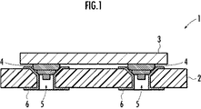
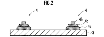
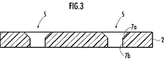
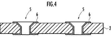
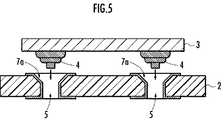
【解決手段】電子部品3に形成された金バンプ4と、配線パターンを備える配線基板2に形成され金バンプ4が嵌合された貫通孔5と、貫通孔5の内側面を被覆して形成されると共に金バンプ4と配線パターンとを接続する金属メッキ層6とを備える。貫通孔5は、外側ほど大径の開口部7aを備える。電子部品3は能動素子、受動素子または配線パターンを備える配線基板である。電子部品3に金バンプ4を形成する。配線パターンを備える配線基板2に貫通孔5を形成する。貫通孔5の内側面を被覆する金属メッキ層6を形成し、金属メッキ層6と配線パターンとを接続する。電子部品3を配線基板2に重ね合わせ押圧して、金バンプ4を貫通孔5に嵌合させ、電子部品3を配線パターンに接続する。
【選択図】 図1
Description
Claims (5)
- 少なくとも1つの配線パターンと、該配線パターンに接続された電子部品とを備える配線基板において、
該電子部品の該配線基板に対向する面に形成された少なくとも1つの金バンプと、該配線基板の該電子部品との接続を必要とする位置に形成され該金バンプが嵌合された貫通孔と、該貫通孔の内側面を被覆して形成されると共に該金バンプと該配線パターンとを接続する金属メッキ層とを備えることを特徴とする配線基板。 - 請求項1記載の配線基板において、前記貫通孔は、前記金バンプに対向する側に、外側ほど大径となっている開口部を備えていることを特徴とする配線基板。
- 請求項1または請求項2記載の配線基板において、前記電子部品は能動素子または受動素子であることを特徴とする配線基板。
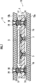
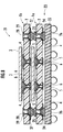
- 請求項1または請求項2記載の配線基板において、前記電子部品は配線パターンを備える配線基板であることを特徴とする配線基板。
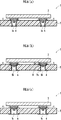
- 電子部品の配線基板に対向する面に少なくとも1つの金バンプを形成する工程と、
少なくとも1つの配線パターンを備える配線基板の該電子部品との接続を必要とする位置に貫通孔を形成する工程と、
該貫通孔の内側面を被覆する金属メッキ層を形成し、該金属メッキ層と該配線パターンとを接続する工程と、
該電子部品を該配線基板に重ね合わせて押圧することにより、該金バンプを該貫通孔に嵌合させ、該電子部品を該配線パターンに接続する工程とを備えることを特徴とする配線基板の製造方法。
Priority Applications (1)
| Application Number | Priority Date | Filing Date | Title |
|---|---|---|---|
| JP2007124276A JP4759753B2 (ja) | 2007-05-09 | 2007-05-09 | 配線基板及びその製造方法 |
Applications Claiming Priority (1)
| Application Number | Priority Date | Filing Date | Title |
|---|---|---|---|
| JP2007124276A JP4759753B2 (ja) | 2007-05-09 | 2007-05-09 | 配線基板及びその製造方法 |
Publications (2)
| Publication Number | Publication Date |
|---|---|
| JP2008282902A true JP2008282902A (ja) | 2008-11-20 |
| JP4759753B2 JP4759753B2 (ja) | 2011-08-31 |
Family
ID=40143491
Family Applications (1)
| Application Number | Title | Priority Date | Filing Date |
|---|---|---|---|
| JP2007124276A Expired - Fee Related JP4759753B2 (ja) | 2007-05-09 | 2007-05-09 | 配線基板及びその製造方法 |
Country Status (1)
| Country | Link |
|---|---|
| JP (1) | JP4759753B2 (ja) |
Cited By (2)
| Publication number | Priority date | Publication date | Assignee | Title |
|---|---|---|---|---|
| JP2010187133A (ja) * | 2009-02-10 | 2010-08-26 | Seiko Epson Corp | 電子部品の実装構造、及び電子部品の実装方法 |
| WO2020255745A1 (ja) * | 2019-06-19 | 2020-12-24 | Tdk株式会社 | センサー用パッケージ基板及びこれを備えるセンサーモジュール、並びに、センサー用パッケージ基板の製造方法 |
Citations (5)
| Publication number | Priority date | Publication date | Assignee | Title |
|---|---|---|---|---|
| JPH05129370A (ja) * | 1991-11-07 | 1993-05-25 | Fujitsu General Ltd | チツプ部品取付構造 |
| JPH08222599A (ja) * | 1995-02-13 | 1996-08-30 | Mitsubishi Electric Corp | 電子部品の実装方法 |
| JP2002033349A (ja) * | 2001-06-07 | 2002-01-31 | Matsushita Electric Ind Co Ltd | 半導体素子の実装方法、及び回路基板 |
| JP2002076055A (ja) * | 2000-08-22 | 2002-03-15 | Hitachi Ltd | 半導体装置の実装方法および実装構造 |
| JP2004247621A (ja) * | 2003-02-17 | 2004-09-02 | Renesas Technology Corp | 半導体装置およびその製造方法 |
-
2007
- 2007-05-09 JP JP2007124276A patent/JP4759753B2/ja not_active Expired - Fee Related
Patent Citations (5)
| Publication number | Priority date | Publication date | Assignee | Title |
|---|---|---|---|---|
| JPH05129370A (ja) * | 1991-11-07 | 1993-05-25 | Fujitsu General Ltd | チツプ部品取付構造 |
| JPH08222599A (ja) * | 1995-02-13 | 1996-08-30 | Mitsubishi Electric Corp | 電子部品の実装方法 |
| JP2002076055A (ja) * | 2000-08-22 | 2002-03-15 | Hitachi Ltd | 半導体装置の実装方法および実装構造 |
| JP2002033349A (ja) * | 2001-06-07 | 2002-01-31 | Matsushita Electric Ind Co Ltd | 半導体素子の実装方法、及び回路基板 |
| JP2004247621A (ja) * | 2003-02-17 | 2004-09-02 | Renesas Technology Corp | 半導体装置およびその製造方法 |
Cited By (5)
| Publication number | Priority date | Publication date | Assignee | Title |
|---|---|---|---|---|
| JP2010187133A (ja) * | 2009-02-10 | 2010-08-26 | Seiko Epson Corp | 電子部品の実装構造、及び電子部品の実装方法 |
| WO2020255745A1 (ja) * | 2019-06-19 | 2020-12-24 | Tdk株式会社 | センサー用パッケージ基板及びこれを備えるセンサーモジュール、並びに、センサー用パッケージ基板の製造方法 |
| JP2021001732A (ja) * | 2019-06-19 | 2021-01-07 | Tdk株式会社 | センサー用パッケージ基板及びこれを備えるセンサーモジュール、並びに、センサー用パッケージ基板の製造方法 |
| JP7207192B2 (ja) | 2019-06-19 | 2023-01-18 | Tdk株式会社 | センサー用パッケージ基板及びこれを備えるセンサーモジュール、並びに、センサー用パッケージ基板の製造方法 |
| US12240751B2 (en) | 2019-06-19 | 2025-03-04 | Tdk Corporation | Sensor package substrate, sensor module having the same, and sensor package substrate manufacturing method |
Also Published As
| Publication number | Publication date |
|---|---|
| JP4759753B2 (ja) | 2011-08-31 |
Similar Documents
| Publication | Publication Date | Title |
|---|---|---|
| JP2595909B2 (ja) | 半導体装置 | |
| TWI458415B (zh) | 多層印刷配線板及其製造方法 | |
| JP5018483B2 (ja) | 電子デバイスパッケージ、モジュール、および電子機器 | |
| JP5018826B2 (ja) | 電子デバイスおよびその製造方法 | |
| KR100459971B1 (ko) | 반도체 장치 및 그 제조 방법, 제조 장치, 회로 기판 및전자기기 | |
| JP4431123B2 (ja) | 電子装置用基板およびその製造方法、並びに電子装置およびその製造方法 | |
| TWI459871B (zh) | Built-in parts wiring board, built-in parts wiring board manufacturing methods | |
| KR101696705B1 (ko) | 칩 내장형 pcb 및 그 제조 방법과, 그 적층 패키지 | |
| US7749806B2 (en) | Fabricating process of a chip package structure | |
| KR20060063654A (ko) | 칩 내장 기판의 제조 방법 | |
| US20100059876A1 (en) | Electronic component package and method of manufacturing the same | |
| JPWO2001026147A1 (ja) | 半導体装置及びその製造方法、回路基板並びに電子機器 | |
| JP2008226945A (ja) | 半導体装置およびその製造方法 | |
| JP2011249759A (ja) | 電子素子内蔵印刷回路基板及びその製造方法 | |
| JP2009141169A (ja) | 半導体装置 | |
| TW201413842A (zh) | 層疊封裝結構及其製作方法 | |
| JP2008288489A (ja) | チップ内蔵基板の製造方法 | |
| JP2017034059A (ja) | プリント配線板、半導体パッケージおよびプリント配線板の製造方法 | |
| JP2009200313A (ja) | Pga型配線基板及びその製造方法 | |
| US8125081B2 (en) | Semiconductor device, printed wiring board for mounting the semiconductor device and connecting structure for these | |
| JP2009267163A (ja) | 配線基板、半導体装置、ならびに半導体装置の製造方法 | |
| JP2006134912A (ja) | 半導体モジュールおよびその製造方法、ならびにフィルムインターポーザ | |
| JP2009135391A (ja) | 電子装置およびその製造方法 | |
| US7759795B2 (en) | Printed circuit board having reliable bump interconnection structure, method of fabricating the same, and semiconductor package using the same | |
| JP4759753B2 (ja) | 配線基板及びその製造方法 |
Legal Events
| Date | Code | Title | Description |
|---|---|---|---|
| A621 | Written request for application examination |
Free format text: JAPANESE INTERMEDIATE CODE: A621 Effective date: 20090127 |
|
| A977 | Report on retrieval |
Free format text: JAPANESE INTERMEDIATE CODE: A971007 Effective date: 20110217 |
|
| A131 | Notification of reasons for refusal |
Free format text: JAPANESE INTERMEDIATE CODE: A131 Effective date: 20110222 |
|
| A521 | Request for written amendment filed |
Free format text: JAPANESE INTERMEDIATE CODE: A523 Effective date: 20110411 |
|
| TRDD | Decision of grant or rejection written | ||
| A01 | Written decision to grant a patent or to grant a registration (utility model) |
Free format text: JAPANESE INTERMEDIATE CODE: A01 Effective date: 20110510 |
|
| A61 | First payment of annual fees (during grant procedure) |
Free format text: JAPANESE INTERMEDIATE CODE: A61 Effective date: 20110513 |
|
| FPAY | Renewal fee payment (event date is renewal date of database) |
Free format text: PAYMENT UNTIL: 20140617 Year of fee payment: 3 |
|
| R150 | Certificate of patent or registration of utility model |
Free format text: JAPANESE INTERMEDIATE CODE: R150 Ref document number: 4759753 Country of ref document: JP Free format text: JAPANESE INTERMEDIATE CODE: R150 |
|
| R250 | Receipt of annual fees |
Free format text: JAPANESE INTERMEDIATE CODE: R250 |
|
| R250 | Receipt of annual fees |
Free format text: JAPANESE INTERMEDIATE CODE: R250 |
|
| R250 | Receipt of annual fees |
Free format text: JAPANESE INTERMEDIATE CODE: R250 |
|
| R250 | Receipt of annual fees |
Free format text: JAPANESE INTERMEDIATE CODE: R250 |
|
| R250 | Receipt of annual fees |
Free format text: JAPANESE INTERMEDIATE CODE: R250 |
|
| R250 | Receipt of annual fees |
Free format text: JAPANESE INTERMEDIATE CODE: R250 |
|
| LAPS | Cancellation because of no payment of annual fees |