JP2008226389A - 半導体記憶装置 - Google Patents
半導体記憶装置 Download PDFInfo
- Publication number
- JP2008226389A JP2008226389A JP2007066084A JP2007066084A JP2008226389A JP 2008226389 A JP2008226389 A JP 2008226389A JP 2007066084 A JP2007066084 A JP 2007066084A JP 2007066084 A JP2007066084 A JP 2007066084A JP 2008226389 A JP2008226389 A JP 2008226389A
- Authority
- JP
- Japan
- Prior art keywords
- memory device
- semiconductor memory
- mode
- relief
- circuit
- Prior art date
- Legal status (The legal status is an assumption and is not a legal conclusion. Google has not performed a legal analysis and makes no representation as to the accuracy of the status listed.)
- Pending
Links
Images


Classifications
-
- G—PHYSICS
- G11—INFORMATION STORAGE
- G11C—STATIC STORES
- G11C29/00—Checking stores for correct operation ; Subsequent repair; Testing stores during standby or offline operation
- G11C29/70—Masking faults in memories by using spares or by reconfiguring
- G11C29/78—Masking faults in memories by using spares or by reconfiguring using programmable devices
- G11C29/84—Masking faults in memories by using spares or by reconfiguring using programmable devices with improved access time or stability
-
- G—PHYSICS
- G11—INFORMATION STORAGE
- G11C—STATIC STORES
- G11C29/00—Checking stores for correct operation ; Subsequent repair; Testing stores during standby or offline operation
- G11C29/70—Masking faults in memories by using spares or by reconfiguring
- G11C29/78—Masking faults in memories by using spares or by reconfiguring using programmable devices
- G11C29/785—Masking faults in memories by using spares or by reconfiguring using programmable devices with redundancy programming schemes
- G11C29/787—Masking faults in memories by using spares or by reconfiguring using programmable devices with redundancy programming schemes using a fuse hierarchy
Abstract
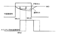
【解決手段】 救済回路を備える半導体記憶装置において、前記救済回路が、複数種の不良に対応する複数の救済モードのうちのひとつを選択するためのモードフューズを備え、複数種類のマージン性不良を救済できる半導体記憶装置を提供する。すなわち物理的に壊れている場合は冗長置換で救済し、マージン不良の場合は、タイミング調整で救済する。
【選択図】図1
Description
12 行デコーダ
13 列デコーダ
14 行デコーダ制御調整回路
15 列デコーダ制御調整回路
16 行救済判定回路
17 列救済判定回路
18 制御回路
161,171 アドレスフューズ群
162,172 モード・調整フューズ群
41 第1のクロックドインバータ
42 第2のクロックドインバータ
43 遅延回路
51 YSW起動回路
52 MA起動回路
53,54 遅延回路
61−1〜61−n 排他的論理和ゲート
62 イネーブル線
63 アンドゲート
64 アドレス比較回路
65−1,65−2 アンドゲート
66 モード選択・調整回路
Claims (6)
- 救済回路を備える半導体記憶装置において、
前記救済回路が、複数種の不良に対応する複数の救済モードのうちのひとつを選択するためのモードフューズを備えていることを特徴とする半導体記憶装置。 - 請求項1に記載された半導体記憶装置において、
前記救済回路が、救済対象アドレスを指定するためのアドレスフューズと、該アドレスフューズにより指定されるアドレスと入力アドレスとを比較して比較結果を出力する比較部とを含むアドレス比較回路と、
前記モードフューズを含み、前記比較結果を受けて前記モードフューズにより選択される救済モードに応じた救済信号を出力する調整回路と、
を有することを特徴とする半導体記憶装置。 - 請求項2に記載された半導体記憶装置において、
前記モードフューズが、マージン性不良を救済するための信号タイミングの調整を行うタイミング調整フューズを兼ねていることを特徴とする半導体記憶装置。 - 請求項2又は3に記載の半導体記憶装置において、
伝送遅延時間の異なる2つの経路と、前記救済信号に応じて前記2つの経路の一方の経路を導通させるゲート回路とをさらに備えることを特徴とする半導体記憶装置。 - 請求項1乃至4のいずれか一つに記載の半導体記憶装置において、
前記救済モードには、メインアンプ起動タイミング不良、書き込みマージン不足による不良及び読み出しマージン不足による不良のうちの少なくとも一つの不良を救済するモードが含まれることを特徴とする半導体記憶装置。 - 請求項1又は2に記載の半導体記憶装置において、
前記救済モードには、物理的不良を救済するモードが含まれることを特徴とする半導体記憶装置。
Priority Applications (2)
| Application Number | Priority Date | Filing Date | Title |
|---|---|---|---|
| JP2007066084A JP2008226389A (ja) | 2007-03-15 | 2007-03-15 | 半導体記憶装置 |
| US12/076,063 US7826295B2 (en) | 2007-03-15 | 2008-03-13 | Semiconductor memory device including a repair circuit which includes mode fuses |
Applications Claiming Priority (1)
| Application Number | Priority Date | Filing Date | Title |
|---|---|---|---|
| JP2007066084A JP2008226389A (ja) | 2007-03-15 | 2007-03-15 | 半導体記憶装置 |
Publications (2)
| Publication Number | Publication Date |
|---|---|
| JP2008226389A true JP2008226389A (ja) | 2008-09-25 |
| JP2008226389A5 JP2008226389A5 (ja) | 2010-10-14 |
Family
ID=39762504
Family Applications (1)
| Application Number | Title | Priority Date | Filing Date |
|---|---|---|---|
| JP2007066084A Pending JP2008226389A (ja) | 2007-03-15 | 2007-03-15 | 半導体記憶装置 |
Country Status (2)
| Country | Link |
|---|---|
| US (1) | US7826295B2 (ja) |
| JP (1) | JP2008226389A (ja) |
Cited By (1)
| Publication number | Priority date | Publication date | Assignee | Title |
|---|---|---|---|---|
| EP2161331A1 (en) | 2008-09-03 | 2010-03-10 | Nishikawa Rubber Co., Ltd. | Thermostable duplex-specific nuclease |
Families Citing this family (2)
| Publication number | Priority date | Publication date | Assignee | Title |
|---|---|---|---|---|
| US8516408B2 (en) * | 2009-05-26 | 2013-08-20 | Lsi Corporation | Optimization of circuits having repeatable circuit instances |
| KR101877818B1 (ko) * | 2012-05-30 | 2018-07-13 | 에스케이하이닉스 주식회사 | 리페어 제어 회로 및 이를 이용한 반도체 집적회로 |
Citations (4)
| Publication number | Priority date | Publication date | Assignee | Title |
|---|---|---|---|---|
| JPH10177792A (ja) * | 1996-09-03 | 1998-06-30 | Townsend & Townsend & Crew Llp | センスアンプタイミング回路 |
| JP2002074961A (ja) * | 2000-08-28 | 2002-03-15 | Mitsubishi Electric Corp | 半導体記憶装置 |
| JP2002216481A (ja) * | 2001-01-19 | 2002-08-02 | Hitachi Ltd | 半導体集積回路装置 |
| JP2004164737A (ja) * | 2002-11-12 | 2004-06-10 | Hitachi Ltd | 半導体集積回路装置と救済方法 |
Family Cites Families (6)
| Publication number | Priority date | Publication date | Assignee | Title |
|---|---|---|---|---|
| US6324103B2 (en) * | 1998-11-11 | 2001-11-27 | Hitachi, Ltd. | Semiconductor integrated circuit device, memory module, storage device and the method for repairing semiconductor integrated circuit device |
| JP2002208294A (ja) * | 2001-01-12 | 2002-07-26 | Toshiba Corp | リダンダンシーシステムを有する半導体記憶装置 |
| US7152187B2 (en) * | 2003-11-26 | 2006-12-19 | Texas Instruments Incorporated | Low-power SRAM E-fuse repair methodology |
| KR100817069B1 (ko) * | 2006-10-26 | 2008-03-27 | 삼성전자주식회사 | 퓨즈 박스의 퓨즈 배치 방법 및 그 방법을 사용하는 반도체메모리 장치 |
| KR20080090664A (ko) * | 2007-04-05 | 2008-10-09 | 삼성전자주식회사 | 포스트 패키지 리페어 제어회로를 구비하는 반도체메모리장치 및 포스트 패키지 리페어 방법 |
| KR20090084531A (ko) * | 2008-02-01 | 2009-08-05 | 삼성전자주식회사 | 퓨즈 회로 및 이를 포함하는 반도체 메모리 장치 |
-
2007
- 2007-03-15 JP JP2007066084A patent/JP2008226389A/ja active Pending
-
2008
- 2008-03-13 US US12/076,063 patent/US7826295B2/en not_active Expired - Fee Related
Patent Citations (4)
| Publication number | Priority date | Publication date | Assignee | Title |
|---|---|---|---|---|
| JPH10177792A (ja) * | 1996-09-03 | 1998-06-30 | Townsend & Townsend & Crew Llp | センスアンプタイミング回路 |
| JP2002074961A (ja) * | 2000-08-28 | 2002-03-15 | Mitsubishi Electric Corp | 半導体記憶装置 |
| JP2002216481A (ja) * | 2001-01-19 | 2002-08-02 | Hitachi Ltd | 半導体集積回路装置 |
| JP2004164737A (ja) * | 2002-11-12 | 2004-06-10 | Hitachi Ltd | 半導体集積回路装置と救済方法 |
Cited By (1)
| Publication number | Priority date | Publication date | Assignee | Title |
|---|---|---|---|---|
| EP2161331A1 (en) | 2008-09-03 | 2010-03-10 | Nishikawa Rubber Co., Ltd. | Thermostable duplex-specific nuclease |
Also Published As
| Publication number | Publication date |
|---|---|
| US20080225620A1 (en) | 2008-09-18 |
| US7826295B2 (en) | 2010-11-02 |
Similar Documents
| Publication | Publication Date | Title |
|---|---|---|
| US7224596B2 (en) | Apparatus and method for repairing semiconductor memory device | |
| US8315116B2 (en) | Repair circuit and repair method of semiconductor memory apparatus | |
| US7257037B2 (en) | Redundancy circuit in semiconductor memory device | |
| US7221604B2 (en) | Memory structure with repairing function and repairing method thereof | |
| US8601327B2 (en) | Semiconductor memory device | |
| JPH0358399A (ja) | 半導体記憶装置 | |
| JP4824083B2 (ja) | 半導体メモリ | |
| US20050232036A1 (en) | Semiconductor memory device and method of driving the same | |
| JP2008226389A (ja) | 半導体記憶装置 | |
| US20180308563A1 (en) | Memory device including repair circuit and operation method thereof | |
| JP4891748B2 (ja) | 半導体集積回路およびそのテスト方法 | |
| US8059477B2 (en) | Redundancy circuit of semiconductor memory | |
| US9589668B2 (en) | Semiconductor memory device for performing test operation of circuits related to repair scheme and operating method thereof | |
| KR100944325B1 (ko) | 리페어 퓨즈 장치 | |
| US6535436B2 (en) | Redundant circuit and method for replacing defective memory cells in a memory device | |
| JP4125542B2 (ja) | 半導体記憶装置およびその製造方法 | |
| JP2005285281A (ja) | 半導体記憶装置及び半導体記憶装置の製造方法 | |
| US20040208065A1 (en) | Row redundancy memory repair scheme with shift ot eliminate timing penalty | |
| US20040076042A1 (en) | High performance memory column group repair scheme with small area penalty | |
| JP2003100094A (ja) | 半導体記憶装置 | |
| JP5074968B2 (ja) | 集積回路及びメモリテスト方法 | |
| KR100871691B1 (ko) | 병렬 비트 테스트 방법 및 그 방법을 사용하는 반도체메모리 장치 | |
| KR20030058256A (ko) | 플래시 메모리 소자 및 그의 리페어 방법 | |
| KR20090013620A (ko) | 리페어 회로 | |
| KR20070038672A (ko) | 반도체 메모리 장치의 칼럼 리페어 회로 |
Legal Events
| Date | Code | Title | Description |
|---|---|---|---|
| A621 | Written request for application examination |
Free format text: JAPANESE INTERMEDIATE CODE: A621 Effective date: 20100215 |
|
| A521 | Written amendment |
Free format text: JAPANESE INTERMEDIATE CODE: A523 Effective date: 20100825 |
|
| A977 | Report on retrieval |
Free format text: JAPANESE INTERMEDIATE CODE: A971007 Effective date: 20120302 |
|
| A131 | Notification of reasons for refusal |
Free format text: JAPANESE INTERMEDIATE CODE: A131 Effective date: 20120314 |
|
| A711 | Notification of change in applicant |
Free format text: JAPANESE INTERMEDIATE CODE: A711 Effective date: 20140214 |
|
| A02 | Decision of refusal |
Free format text: JAPANESE INTERMEDIATE CODE: A02 Effective date: 20140507 |