JP2007522673A - 処理済みフォトレジストを使用して半導体素子を形成する方法 - Google Patents
処理済みフォトレジストを使用して半導体素子を形成する方法 Download PDFInfo
- Publication number
- JP2007522673A JP2007522673A JP2006553127A JP2006553127A JP2007522673A JP 2007522673 A JP2007522673 A JP 2007522673A JP 2006553127 A JP2006553127 A JP 2006553127A JP 2006553127 A JP2006553127 A JP 2006553127A JP 2007522673 A JP2007522673 A JP 2007522673A
- Authority
- JP
- Japan
- Prior art keywords
- layer
- photoresist layer
- photoresist
- patterned
- patterned photoresist
- Prior art date
- Legal status (The legal status is an assumption and is not a legal conclusion. Google has not performed a legal analysis and makes no representation as to the accuracy of the status listed.)
- Pending
Links
- 229920002120 photoresistant polymer Polymers 0.000 title claims abstract description 98
- 238000000034 method Methods 0.000 title claims abstract description 48
- 239000004065 semiconductor Substances 0.000 title claims abstract description 31
- 230000008569 process Effects 0.000 claims abstract description 24
- 238000000059 patterning Methods 0.000 claims abstract description 7
- 238000005530 etching Methods 0.000 claims description 23
- 238000009966 trimming Methods 0.000 claims description 13
- 238000003682 fluorination reaction Methods 0.000 claims description 12
- 239000000758 substrate Substances 0.000 claims description 11
- 230000026030 halogenation Effects 0.000 claims description 6
- 238000005658 halogenation reaction Methods 0.000 claims description 6
- 239000000463 material Substances 0.000 claims description 5
- 238000004519 manufacturing process Methods 0.000 claims description 4
- 238000006243 chemical reaction Methods 0.000 claims description 3
- 230000002829 reductive effect Effects 0.000 claims description 3
- QVGXLLKOCUKJST-UHFFFAOYSA-N atomic oxygen Chemical compound [O] QVGXLLKOCUKJST-UHFFFAOYSA-N 0.000 claims description 2
- 239000004020 conductor Substances 0.000 claims description 2
- 239000001301 oxygen Substances 0.000 claims description 2
- 229910052760 oxygen Inorganic materials 0.000 claims description 2
- 238000005660 chlorination reaction Methods 0.000 claims 4
- 238000001020 plasma etching Methods 0.000 claims 2
- 239000000126 substance Substances 0.000 claims 2
- 238000001311 chemical methods and process Methods 0.000 claims 1
- 239000011810 insulating material Substances 0.000 claims 1
- 238000010849 ion bombardment Methods 0.000 claims 1
- 238000010297 mechanical methods and process Methods 0.000 claims 1
- 230000005226 mechanical processes and functions Effects 0.000 claims 1
- 230000000704 physical effect Effects 0.000 claims 1
- 230000001737 promoting effect Effects 0.000 claims 1
- 230000001629 suppression Effects 0.000 claims 1
- 229910052731 fluorine Inorganic materials 0.000 abstract description 30
- 239000011737 fluorine Substances 0.000 abstract description 30
- 229910052736 halogen Inorganic materials 0.000 abstract description 5
- 150000002367 halogens Chemical class 0.000 abstract description 5
- ZAMOUSCENKQFHK-UHFFFAOYSA-N Chlorine atom Chemical compound [Cl] ZAMOUSCENKQFHK-UHFFFAOYSA-N 0.000 abstract description 4
- 239000000460 chlorine Substances 0.000 abstract description 4
- 229910052801 chlorine Inorganic materials 0.000 abstract description 4
- PXGOKWXKJXAPGV-UHFFFAOYSA-N Fluorine Chemical compound FF PXGOKWXKJXAPGV-UHFFFAOYSA-N 0.000 abstract 2
- YCKRFDGAMUMZLT-UHFFFAOYSA-N Fluorine atom Chemical compound [F] YCKRFDGAMUMZLT-UHFFFAOYSA-N 0.000 description 28
- 229910021420 polycrystalline silicon Inorganic materials 0.000 description 6
- 229920005591 polysilicon Polymers 0.000 description 6
- 230000008901 benefit Effects 0.000 description 5
- 230000000694 effects Effects 0.000 description 4
- 230000002411 adverse Effects 0.000 description 3
- 230000015572 biosynthetic process Effects 0.000 description 3
- 125000001153 fluoro group Chemical group F* 0.000 description 3
- XKRFYHLGVUSROY-UHFFFAOYSA-N Argon Chemical compound [Ar] XKRFYHLGVUSROY-UHFFFAOYSA-N 0.000 description 2
- IJGRMHOSHXDMSA-UHFFFAOYSA-N Atomic nitrogen Chemical compound N#N IJGRMHOSHXDMSA-UHFFFAOYSA-N 0.000 description 2
- UFHFLCQGNIYNRP-UHFFFAOYSA-N Hydrogen Chemical compound [H][H] UFHFLCQGNIYNRP-UHFFFAOYSA-N 0.000 description 2
- CPELXLSAUQHCOX-UHFFFAOYSA-N Hydrogen bromide Chemical compound Br CPELXLSAUQHCOX-UHFFFAOYSA-N 0.000 description 2
- 239000006117 anti-reflective coating Substances 0.000 description 2
- 230000008859 change Effects 0.000 description 2
- 239000007789 gas Substances 0.000 description 2
- 239000001257 hydrogen Substances 0.000 description 2
- 229910052739 hydrogen Inorganic materials 0.000 description 2
- 125000004435 hydrogen atom Chemical group [H]* 0.000 description 2
- 238000005259 measurement Methods 0.000 description 2
- 239000002184 metal Substances 0.000 description 2
- 230000036961 partial effect Effects 0.000 description 2
- 238000005549 size reduction Methods 0.000 description 2
- 229910052786 argon Inorganic materials 0.000 description 1
- 230000007547 defect Effects 0.000 description 1
- 238000001312 dry etching Methods 0.000 description 1
- 125000005843 halogen group Chemical group 0.000 description 1
- 230000009931 harmful effect Effects 0.000 description 1
- 229910000042 hydrogen bromide Inorganic materials 0.000 description 1
- 230000006872 improvement Effects 0.000 description 1
- 230000000977 initiatory effect Effects 0.000 description 1
- 230000000670 limiting effect Effects 0.000 description 1
- 238000001459 lithography Methods 0.000 description 1
- 230000004048 modification Effects 0.000 description 1
- 238000012986 modification Methods 0.000 description 1
- 229910052757 nitrogen Inorganic materials 0.000 description 1
- 230000000149 penetrating effect Effects 0.000 description 1
- 238000000206 photolithography Methods 0.000 description 1
- 239000003223 protective agent Substances 0.000 description 1
- 125000006850 spacer group Chemical group 0.000 description 1
Images


Classifications
-
- H—ELECTRICITY
- H01—ELECTRIC ELEMENTS
- H01L—SEMICONDUCTOR DEVICES NOT COVERED BY CLASS H10
- H01L21/00—Processes or apparatus adapted for the manufacture or treatment of semiconductor or solid state devices or of parts thereof
- H01L21/02—Manufacture or treatment of semiconductor devices or of parts thereof
- H01L21/027—Making masks on semiconductor bodies for further photolithographic processing not provided for in group H01L21/18 or H01L21/34
- H01L21/0271—Making masks on semiconductor bodies for further photolithographic processing not provided for in group H01L21/18 or H01L21/34 comprising organic layers
- H01L21/0273—Making masks on semiconductor bodies for further photolithographic processing not provided for in group H01L21/18 or H01L21/34 comprising organic layers characterised by the treatment of photoresist layers
-
- B—PERFORMING OPERATIONS; TRANSPORTING
- B82—NANOTECHNOLOGY
- B82Y—SPECIFIC USES OR APPLICATIONS OF NANOSTRUCTURES; MEASUREMENT OR ANALYSIS OF NANOSTRUCTURES; MANUFACTURE OR TREATMENT OF NANOSTRUCTURES
- B82Y40/00—Manufacture or treatment of nanostructures
-
- G—PHYSICS
- G03—PHOTOGRAPHY; CINEMATOGRAPHY; ANALOGOUS TECHNIQUES USING WAVES OTHER THAN OPTICAL WAVES; ELECTROGRAPHY; HOLOGRAPHY
- G03F—PHOTOMECHANICAL PRODUCTION OF TEXTURED OR PATTERNED SURFACES, e.g. FOR PRINTING, FOR PROCESSING OF SEMICONDUCTOR DEVICES; MATERIALS THEREFOR; ORIGINALS THEREFOR; APPARATUS SPECIALLY ADAPTED THEREFOR
- G03F7/00—Photomechanical, e.g. photolithographic, production of textured or patterned surfaces, e.g. printing surfaces; Materials therefor, e.g. comprising photoresists; Apparatus specially adapted therefor
- G03F7/26—Processing photosensitive materials; Apparatus therefor
-
- H—ELECTRICITY
- H01—ELECTRIC ELEMENTS
- H01L—SEMICONDUCTOR DEVICES NOT COVERED BY CLASS H10
- H01L21/00—Processes or apparatus adapted for the manufacture or treatment of semiconductor or solid state devices or of parts thereof
- H01L21/02—Manufacture or treatment of semiconductor devices or of parts thereof
- H01L21/04—Manufacture or treatment of semiconductor devices or of parts thereof the devices having potential barriers, e.g. a PN junction, depletion layer or carrier concentration layer
- H01L21/18—Manufacture or treatment of semiconductor devices or of parts thereof the devices having potential barriers, e.g. a PN junction, depletion layer or carrier concentration layer the devices having semiconductor bodies comprising elements of Group IV of the Periodic Table or AIIIBV compounds with or without impurities, e.g. doping materials
- H01L21/28—Manufacture of electrodes on semiconductor bodies using processes or apparatus not provided for in groups H01L21/20 - H01L21/268
- H01L21/28008—Making conductor-insulator-semiconductor electrodes
- H01L21/28017—Making conductor-insulator-semiconductor electrodes the insulator being formed after the semiconductor body, the semiconductor being silicon
- H01L21/28026—Making conductor-insulator-semiconductor electrodes the insulator being formed after the semiconductor body, the semiconductor being silicon characterised by the conductor
- H01L21/28123—Lithography-related aspects, e.g. sub-lithography lengths; Isolation-related aspects, e.g. to solve problems arising at the crossing with the side of the device isolation; Planarisation aspects
-
- H—ELECTRICITY
- H01—ELECTRIC ELEMENTS
- H01L—SEMICONDUCTOR DEVICES NOT COVERED BY CLASS H10
- H01L21/00—Processes or apparatus adapted for the manufacture or treatment of semiconductor or solid state devices or of parts thereof
- H01L21/02—Manufacture or treatment of semiconductor devices or of parts thereof
- H01L21/04—Manufacture or treatment of semiconductor devices or of parts thereof the devices having potential barriers, e.g. a PN junction, depletion layer or carrier concentration layer
- H01L21/18—Manufacture or treatment of semiconductor devices or of parts thereof the devices having potential barriers, e.g. a PN junction, depletion layer or carrier concentration layer the devices having semiconductor bodies comprising elements of Group IV of the Periodic Table or AIIIBV compounds with or without impurities, e.g. doping materials
- H01L21/30—Treatment of semiconductor bodies using processes or apparatus not provided for in groups H01L21/20 - H01L21/26
- H01L21/31—Treatment of semiconductor bodies using processes or apparatus not provided for in groups H01L21/20 - H01L21/26 to form insulating layers thereon, e.g. for masking or by using photolithographic techniques; After treatment of these layers; Selection of materials for these layers
- H01L21/3205—Deposition of non-insulating-, e.g. conductive- or resistive-, layers on insulating layers; After-treatment of these layers
- H01L21/321—After treatment
- H01L21/3213—Physical or chemical etching of the layers, e.g. to produce a patterned layer from a pre-deposited extensive layer
- H01L21/32139—Physical or chemical etching of the layers, e.g. to produce a patterned layer from a pre-deposited extensive layer using masks
-
- H—ELECTRICITY
- H01—ELECTRIC ELEMENTS
- H01L—SEMICONDUCTOR DEVICES NOT COVERED BY CLASS H10
- H01L29/00—Semiconductor devices specially adapted for rectifying, amplifying, oscillating or switching and having potential barriers; Capacitors or resistors having potential barriers, e.g. a PN-junction depletion layer or carrier concentration layer; Details of semiconductor bodies or of electrodes thereof ; Multistep manufacturing processes therefor
- H01L29/66—Types of semiconductor device ; Multistep manufacturing processes therefor
- H01L29/66007—Multistep manufacturing processes
- H01L29/66075—Multistep manufacturing processes of devices having semiconductor bodies comprising group 14 or group 13/15 materials
- H01L29/66227—Multistep manufacturing processes of devices having semiconductor bodies comprising group 14 or group 13/15 materials the devices being controllable only by the electric current supplied or the electric potential applied, to an electrode which does not carry the current to be rectified, amplified or switched, e.g. three-terminal devices
- H01L29/66409—Unipolar field-effect transistors
- H01L29/66477—Unipolar field-effect transistors with an insulated gate, i.e. MISFET
-
- H—ELECTRICITY
- H01—ELECTRIC ELEMENTS
- H01L—SEMICONDUCTOR DEVICES NOT COVERED BY CLASS H10
- H01L29/00—Semiconductor devices specially adapted for rectifying, amplifying, oscillating or switching and having potential barriers; Capacitors or resistors having potential barriers, e.g. a PN-junction depletion layer or carrier concentration layer; Details of semiconductor bodies or of electrodes thereof ; Multistep manufacturing processes therefor
- H01L29/66—Types of semiconductor device ; Multistep manufacturing processes therefor
- H01L29/68—Types of semiconductor device ; Multistep manufacturing processes therefor controllable by only the electric current supplied, or only the electric potential applied, to an electrode which does not carry the current to be rectified, amplified or switched
- H01L29/76—Unipolar devices, e.g. field effect transistors
- H01L29/772—Field effect transistors
- H01L29/78—Field effect transistors with field effect produced by an insulated gate
-
- H—ELECTRICITY
- H01—ELECTRIC ELEMENTS
- H01L—SEMICONDUCTOR DEVICES NOT COVERED BY CLASS H10
- H01L21/00—Processes or apparatus adapted for the manufacture or treatment of semiconductor or solid state devices or of parts thereof
- H01L21/02—Manufacture or treatment of semiconductor devices or of parts thereof
- H01L21/027—Making masks on semiconductor bodies for further photolithographic processing not provided for in group H01L21/18 or H01L21/34
- H01L21/033—Making masks on semiconductor bodies for further photolithographic processing not provided for in group H01L21/18 or H01L21/34 comprising inorganic layers
- H01L21/0334—Making masks on semiconductor bodies for further photolithographic processing not provided for in group H01L21/18 or H01L21/34 comprising inorganic layers characterised by their size, orientation, disposition, behaviour, shape, in horizontal or vertical plane
- H01L21/0338—Process specially adapted to improve the resolution of the mask
-
- Y—GENERAL TAGGING OF NEW TECHNOLOGICAL DEVELOPMENTS; GENERAL TAGGING OF CROSS-SECTIONAL TECHNOLOGIES SPANNING OVER SEVERAL SECTIONS OF THE IPC; TECHNICAL SUBJECTS COVERED BY FORMER USPC CROSS-REFERENCE ART COLLECTIONS [XRACs] AND DIGESTS
- Y10—TECHNICAL SUBJECTS COVERED BY FORMER USPC
- Y10S—TECHNICAL SUBJECTS COVERED BY FORMER USPC CROSS-REFERENCE ART COLLECTIONS [XRACs] AND DIGESTS
- Y10S438/00—Semiconductor device manufacturing: process
- Y10S438/942—Masking
- Y10S438/945—Special, e.g. metal
-
- Y—GENERAL TAGGING OF NEW TECHNOLOGICAL DEVELOPMENTS; GENERAL TAGGING OF CROSS-SECTIONAL TECHNOLOGIES SPANNING OVER SEVERAL SECTIONS OF THE IPC; TECHNICAL SUBJECTS COVERED BY FORMER USPC CROSS-REFERENCE ART COLLECTIONS [XRACs] AND DIGESTS
- Y10—TECHNICAL SUBJECTS COVERED BY FORMER USPC
- Y10S—TECHNICAL SUBJECTS COVERED BY FORMER USPC CROSS-REFERENCE ART COLLECTIONS [XRACs] AND DIGESTS
- Y10S438/00—Semiconductor device manufacturing: process
- Y10S438/942—Masking
- Y10S438/947—Subphotolithographic processing
Landscapes
- Engineering & Computer Science (AREA)
- Microelectronics & Electronic Packaging (AREA)
- Power Engineering (AREA)
- Physics & Mathematics (AREA)
- General Physics & Mathematics (AREA)
- Condensed Matter Physics & Semiconductors (AREA)
- Computer Hardware Design (AREA)
- Manufacturing & Machinery (AREA)
- Ceramic Engineering (AREA)
- Chemical & Material Sciences (AREA)
- Nanotechnology (AREA)
- Crystallography & Structural Chemistry (AREA)
- Inorganic Chemistry (AREA)
- Drying Of Semiconductors (AREA)
- Insulated Gate Type Field-Effect Transistor (AREA)
- Photosensitive Polymer And Photoresist Processing (AREA)
Abstract
Description
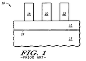
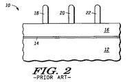
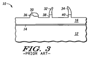
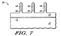
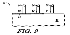
当業者であれば、これらの図における構成要素が説明を簡単かつ明瞭にするために示され、そして必ずしも寸法通りには描かれていないことが分かるであろう。例えば、これらの図における幾つかの構成要素の寸法を他の構成要素に対して誇張して描いて本発明の実施形態を理解し易くしている。
Claims (21)
- 基板を設ける工程と、
パターニングされるべきパターニング対象層を基板の上方に設ける工程と、
最小寸法を有するパターニング済みフォトレジスト層を、前記パターニング対象層の上に設ける工程と、
パターニング済みフォトレジスト層をトリミングする工程と、
フォトレジスト層の特性を改質して後続のエッチング処理に対する耐性を高めるためにトリミング済みのパターニング済みフォトレジスト層を処理する工程と、
トリミング済みのパターニング済みフォトレジスト層のパターンを前記パターニング対象層に転写する工程とを備える、半導体素子の製造方法。 - 前記パターニング対象層は複数の層から成る積層体を含む、請求項1記載の方法。
- 複数の層から成る積層体はパターニング対象の下地層を被覆する犠牲層を含む、請求項2記載の方法。
- トリミングする処理では、最小寸法を機械的処理及び化学的処理の内の少なくとも一つの処理により小さくする、請求項1記載の方法。
- 機械的処理は反応性イオンエッチング(RIE)及びイオン衝撃エッチングの少なくとも一つのエッチングを含む、請求項4記載の方法。
- 化学的処理では、少なくとも酸素と反応させる、請求項4記載の方法。
- 最小寸法は最小寸法の最大80%だけ小さくなる、請求項4記載の方法。
- 最小寸法は約100ナノメートルであり、トリミングによって、最小寸法は約20〜80ナノメートルの範囲に収まるように小さくなる、請求項4記載の方法。
- 前記特性は化学的性質及び物理的性質の内の少なくとも一つを含む、請求項1記載の方法。
- 前記処理はハロゲン化を含む、請求項1記載の方法。
- ハロゲン化は原子を結合させるハロゲン化及び分子を結合させるハロゲン化の内の少なくとも一つを含む、請求項10記載の方法。
- ハロゲン化はフッ化及び塩素化の内の少なくとも一つを含む、請求項10記載の方法。
- 更に、フッ化は原子を結合させるフッ化及び分子を結合させるフッ化の内の少なくとも一つを含む、請求項12記載の方法。
- 更に、塩素化は原子を結合させる塩素化及び分子を結合させる塩素化の内の少なくとも一つを含む、請求項12記載の方法。
- 後続のエッチング処理は少なくとも一つのパターン転写エッチング処理を含む、請求項1記載の方法。
- パターニング済みフォトレジスト層は、第1の大きさの短周期ラインエッジラフネスによって特徴付けられ、そしてトリミング済みのパターニング済みフォトレジスト層を処理することによって、i)短周期ラインエッジラフネスの低減、及びii)更に別の短周期ラインエッジラフネスの抑制の内の少なくとも一つを促進する、請求項1記載の方法。
- 前記トリミング及び前記処理は同じ装置及び個別装置群の内の少なくとも一つにおいて行なわれる、請求項1記載の方法。
- パターニング対象の層は導電材料、半導体材料、及び絶縁材料の内の少なくとも一つを含む、請求項1記載の方法。
- トリミング済みのパターニング済みフォトレジスト層は、トランジスタの制御電極を形成する一部分を含む、請求項1記載の方法。
- 半導体素子であって、
基板と、
基板上に形成される絶縁層と、
絶縁層上に形成される導電層と、
導電層上に形成されるフォトレジスト層とを備え、前記フォトレジスト層はパターニング済みフォトレジスト層からなり、パターニング済みフォトレジスト層は更にトリミング済みのパターニング済みフォトレジスト層を含み、トリミング済みのパターニング済みフォトレジスト層を処理してフォトレジスト層の特性を改質して後続のエッチング処理に対する耐性を高くしている、半導体素子。 - 基板と、基板上に形成される絶縁層と、絶縁層上に形成される導電層と、導電層上に形成され、かつパターニング済みフォトレジスト層を含むフォトレジスト層とを備えた半導体素子を製造するための装置において、
前記パターニング済みフォトレジスト層をトリミングするトリミングモジュールと、
トリミング済みのパターニング済みフォトレジスト層を処理してフォトレジスト層の特性を改質して後続のエッチング処理に対する耐性を高くする処理モジュールとを備える、半導体素子の製造装置。
Applications Claiming Priority (2)
| Application Number | Priority Date | Filing Date | Title |
|---|---|---|---|
| US10/779,007 US7157377B2 (en) | 2004-02-13 | 2004-02-13 | Method of making a semiconductor device using treated photoresist |
| PCT/US2005/000961 WO2005082122A2 (en) | 2004-02-13 | 2005-01-12 | Method of making a semiconductor device using treated photoresist |
Publications (2)
| Publication Number | Publication Date |
|---|---|
| JP2007522673A true JP2007522673A (ja) | 2007-08-09 |
| JP2007522673A5 JP2007522673A5 (ja) | 2008-03-06 |
Family
ID=34838285
Family Applications (1)
| Application Number | Title | Priority Date | Filing Date |
|---|---|---|---|
| JP2006553127A Pending JP2007522673A (ja) | 2004-02-13 | 2005-01-12 | 処理済みフォトレジストを使用して半導体素子を形成する方法 |
Country Status (6)
| Country | Link |
|---|---|
| US (2) | US7157377B2 (ja) |
| EP (1) | EP1719162B8 (ja) |
| JP (1) | JP2007522673A (ja) |
| KR (1) | KR101128260B1 (ja) |
| CN (1) | CN100487873C (ja) |
| WO (1) | WO2005082122A2 (ja) |
Cited By (3)
| Publication number | Priority date | Publication date | Assignee | Title |
|---|---|---|---|---|
| JP2007311508A (ja) * | 2006-05-17 | 2007-11-29 | Nikon Corp | 微細パターン形成方法及びデバイス製造方法 |
| JP2010103497A (ja) * | 2008-09-29 | 2010-05-06 | Tokyo Electron Ltd | マスクパターンの形成方法、微細パターンの形成方法及び成膜装置 |
| JP2015508574A (ja) * | 2012-01-03 | 2015-03-19 | 東京エレクトロン株式会社 | パターン平滑化及びインライン限界寸法のスリム化のための蒸気処理プロセス |
Families Citing this family (10)
| Publication number | Priority date | Publication date | Assignee | Title |
|---|---|---|---|---|
| US20050026084A1 (en) * | 2003-07-31 | 2005-02-03 | Garza Cesar M. | Semiconductor device and method for elimination of resist linewidth slimming by fluorination |
| US8057143B2 (en) * | 2004-10-05 | 2011-11-15 | Fontaine Trailer Company, Inc. | Trailer load securement system |
| US7435354B2 (en) * | 2005-01-06 | 2008-10-14 | United Microelectronic Corp. | Treatment method for surface of photoresist layer and method for forming patterned photoresist layer |
| US8915684B2 (en) | 2005-09-27 | 2014-12-23 | Fontaine Trailer Company, Inc. | Cargo deck |
| US7703826B1 (en) * | 2006-09-08 | 2010-04-27 | German Mark K | Bed liner rail system for cargo holddown |
| CN102573329B (zh) * | 2010-12-08 | 2014-04-02 | 北大方正集团有限公司 | 制作电路板导电柱的方法、系统以及电路板 |
| WO2012173698A1 (en) * | 2011-06-15 | 2012-12-20 | Applied Materials, Inc. | Methods and apparatus for controlling photoresist line width roughness with enhanced electron spin control |
| JP2015115599A (ja) * | 2013-12-13 | 2015-06-22 | 株式会社東芝 | パターン形成方法 |
| EP3719576A1 (en) * | 2019-04-04 | 2020-10-07 | IMEC vzw | Resistless pattering mask |
| DE102020206696A1 (de) | 2020-05-28 | 2021-12-02 | Robert Bosch Gesellschaft mit beschränkter Haftung | Verfahren und Steuergerät zum Herstellen eines Trägerelements zum Aufnehmen einer Probenflüssigkeit, Trägerelement, Trägermodul und Verfahren zum Verwenden eines Trägerelements |
Citations (5)
| Publication number | Priority date | Publication date | Assignee | Title |
|---|---|---|---|---|
| JPH0831720A (ja) * | 1994-07-13 | 1996-02-02 | Nkk Corp | レジストマスクの形成方法 |
| JPH11251295A (ja) * | 1998-02-27 | 1999-09-17 | Sanyo Electric Co Ltd | 半導体装置及びその製造方法 |
| JP2002305181A (ja) * | 2001-04-06 | 2002-10-18 | Seiko Epson Corp | 半導体装置の製造方法 |
| JP2002343769A (ja) * | 2001-05-16 | 2002-11-29 | Shin Etsu Chem Co Ltd | クロム系フォトマスクの形成方法 |
| JP2004530922A (ja) * | 2001-03-28 | 2004-10-07 | アドバンスト・マイクロ・ディバイシズ・インコーポレイテッド | サブリソグラフィフォトレジストフィーチャーを形成するプロセス |
Family Cites Families (16)
| Publication number | Priority date | Publication date | Assignee | Title |
|---|---|---|---|---|
| US4187331A (en) * | 1978-08-24 | 1980-02-05 | International Business Machines Corp. | Fluorine plasma resist image hardening |
| US5332653A (en) * | 1992-07-01 | 1994-07-26 | Motorola, Inc. | Process for forming a conductive region without photoresist-related reflective notching damage |
| JPH0669190A (ja) * | 1992-08-21 | 1994-03-11 | Fujitsu Ltd | フッ素系樹脂膜の形成方法 |
| US5912187A (en) * | 1993-12-30 | 1999-06-15 | Lucent Technologies Inc. | Method of fabricating circuits |
| EP0911697A3 (en) | 1997-10-22 | 1999-09-15 | Interuniversitair Microelektronica Centrum Vzw | A fluorinated hard mask for micropatterning of polymers |
| JP2000214575A (ja) | 1999-01-26 | 2000-08-04 | Sharp Corp | クロムマスクの形成方法 |
| US6506653B1 (en) * | 2000-03-13 | 2003-01-14 | International Business Machines Corporation | Method using disposable and permanent films for diffusion and implant doping |
| US6815359B2 (en) | 2001-03-28 | 2004-11-09 | Advanced Micro Devices, Inc. | Process for improving the etch stability of ultra-thin photoresist |
| US6716571B2 (en) | 2001-03-28 | 2004-04-06 | Advanced Micro Devices, Inc. | Selective photoresist hardening to facilitate lateral trimming |
| US6589709B1 (en) * | 2001-03-28 | 2003-07-08 | Advanced Micro Devices, Inc. | Process for preventing deformation of patterned photoresist features |
| JP3725811B2 (ja) * | 2001-10-11 | 2005-12-14 | ローム株式会社 | 半導体装置の製造方法 |
| US6790782B1 (en) * | 2001-12-28 | 2004-09-14 | Advanced Micro Devices, Inc. | Process for fabrication of a transistor gate including high-K gate dielectric with in-situ resist trim, gate etch, and high-K dielectric removal |
| US6716570B2 (en) * | 2002-05-23 | 2004-04-06 | Institute Of Microelectronics | Low temperature resist trimming process |
| US6979408B2 (en) * | 2002-12-30 | 2005-12-27 | Intel Corporation | Method and apparatus for photomask fabrication |
| US20050026084A1 (en) | 2003-07-31 | 2005-02-03 | Garza Cesar M. | Semiconductor device and method for elimination of resist linewidth slimming by fluorination |
| US6849515B1 (en) | 2003-09-25 | 2005-02-01 | Freescale Semiconductor, Inc. | Semiconductor process for disposable sidewall spacers |
-
2004
- 2004-02-13 US US10/779,007 patent/US7157377B2/en not_active Expired - Fee Related
-
2005
- 2005-01-12 CN CN200580004804.8A patent/CN100487873C/zh not_active Expired - Fee Related
- 2005-01-12 KR KR1020067016205A patent/KR101128260B1/ko not_active IP Right Cessation
- 2005-01-12 EP EP05711379.7A patent/EP1719162B8/en not_active Not-in-force
- 2005-01-12 WO PCT/US2005/000961 patent/WO2005082122A2/en active Application Filing
- 2005-01-12 JP JP2006553127A patent/JP2007522673A/ja active Pending
- 2005-06-02 US US11/143,295 patent/US20050224455A1/en not_active Abandoned
Patent Citations (5)
| Publication number | Priority date | Publication date | Assignee | Title |
|---|---|---|---|---|
| JPH0831720A (ja) * | 1994-07-13 | 1996-02-02 | Nkk Corp | レジストマスクの形成方法 |
| JPH11251295A (ja) * | 1998-02-27 | 1999-09-17 | Sanyo Electric Co Ltd | 半導体装置及びその製造方法 |
| JP2004530922A (ja) * | 2001-03-28 | 2004-10-07 | アドバンスト・マイクロ・ディバイシズ・インコーポレイテッド | サブリソグラフィフォトレジストフィーチャーを形成するプロセス |
| JP2002305181A (ja) * | 2001-04-06 | 2002-10-18 | Seiko Epson Corp | 半導体装置の製造方法 |
| JP2002343769A (ja) * | 2001-05-16 | 2002-11-29 | Shin Etsu Chem Co Ltd | クロム系フォトマスクの形成方法 |
Cited By (4)
| Publication number | Priority date | Publication date | Assignee | Title |
|---|---|---|---|---|
| JP2007311508A (ja) * | 2006-05-17 | 2007-11-29 | Nikon Corp | 微細パターン形成方法及びデバイス製造方法 |
| JP2010103497A (ja) * | 2008-09-29 | 2010-05-06 | Tokyo Electron Ltd | マスクパターンの形成方法、微細パターンの形成方法及び成膜装置 |
| JP4638550B2 (ja) * | 2008-09-29 | 2011-02-23 | 東京エレクトロン株式会社 | マスクパターンの形成方法、微細パターンの形成方法及び成膜装置 |
| JP2015508574A (ja) * | 2012-01-03 | 2015-03-19 | 東京エレクトロン株式会社 | パターン平滑化及びインライン限界寸法のスリム化のための蒸気処理プロセス |
Also Published As
| Publication number | Publication date |
|---|---|
| EP1719162B8 (en) | 2016-05-11 |
| EP1719162A2 (en) | 2006-11-08 |
| WO2005082122A3 (en) | 2006-02-16 |
| EP1719162B1 (en) | 2016-03-23 |
| US20050224455A1 (en) | 2005-10-13 |
| CN1918700A (zh) | 2007-02-21 |
| US20050181630A1 (en) | 2005-08-18 |
| EP1719162A4 (en) | 2009-05-20 |
| KR101128260B1 (ko) | 2012-03-26 |
| CN100487873C (zh) | 2009-05-13 |
| WO2005082122A2 (en) | 2005-09-09 |
| KR20060114716A (ko) | 2006-11-07 |
| US7157377B2 (en) | 2007-01-02 |
Similar Documents
| Publication | Publication Date | Title |
|---|---|---|
| JP2007522673A (ja) | 処理済みフォトレジストを使用して半導体素子を形成する方法 | |
| KR100995725B1 (ko) | 반도체 장치 제조 방법 | |
| US6803661B2 (en) | Polysilicon processing using an anti-reflective dual layer hardmask for 193 nm lithography | |
| US7214626B2 (en) | Etching process for decreasing mask defect | |
| JP4034164B2 (ja) | 微細パターンの作製方法及び半導体装置の製造方法 | |
| TWI554848B (zh) | 為半導體裝置形成薄膜圖案的方法及其設備 | |
| CN1881078B (zh) | 形成抗蚀刻保护层的方法 | |
| US20070122753A1 (en) | Method for manufacturing semiconductor device | |
| TWI301296B (en) | Method for fabricating a hard mask polysilicon gate | |
| US20130059441A1 (en) | Method for fabricating a semiconductor structure | |
| JP4614995B2 (ja) | 半導体装置の製造方法 | |
| US6379872B1 (en) | Etching of anti-reflective coatings | |
| US20070161255A1 (en) | Method for etching with hardmask | |
| US7199034B1 (en) | Flash memory device and method for fabricating the same | |
| JPH03241829A (ja) | 半導体装置の製造方法 | |
| KR100816210B1 (ko) | 반도체 장치 형성 방법 | |
| US7938972B2 (en) | Fabrication method of electronic device | |
| JPH07226396A (ja) | パターン形成方法 | |
| US11372332B2 (en) | Plasma treatment method to improve photo resist roughness and remove photo resist scum | |
| US20110130008A1 (en) | Method to control critical dimension | |
| TW200414301A (en) | Forming bilayer resist patterns | |
| US7268086B2 (en) | Method for reducing critical dimension and semiconductor etching method | |
| KR20070072693A (ko) | 반도체 소자의 제조방법 | |
| JP2001127038A (ja) | 半導体装置の製造方法 | |
| KR100596882B1 (ko) | 폴리실리콘 게이트 형성 방법 |
Legal Events
| Date | Code | Title | Description |
|---|---|---|---|
| A521 | Request for written amendment filed |
Free format text: JAPANESE INTERMEDIATE CODE: A523 Effective date: 20080115 |
|
| A621 | Written request for application examination |
Free format text: JAPANESE INTERMEDIATE CODE: A621 Effective date: 20080115 |
|
| A977 | Report on retrieval |
Free format text: JAPANESE INTERMEDIATE CODE: A971007 Effective date: 20101112 |
|
| A131 | Notification of reasons for refusal |
Free format text: JAPANESE INTERMEDIATE CODE: A131 Effective date: 20101116 |
|
| A521 | Request for written amendment filed |
Free format text: JAPANESE INTERMEDIATE CODE: A523 Effective date: 20110128 |
|
| A131 | Notification of reasons for refusal |
Free format text: JAPANESE INTERMEDIATE CODE: A131 Effective date: 20110301 |
|
| A601 | Written request for extension of time |
Free format text: JAPANESE INTERMEDIATE CODE: A601 Effective date: 20110601 |
|
| A602 | Written permission of extension of time |
Free format text: JAPANESE INTERMEDIATE CODE: A602 Effective date: 20110608 |
|
| A601 | Written request for extension of time |
Free format text: JAPANESE INTERMEDIATE CODE: A601 Effective date: 20110701 |
|
| A602 | Written permission of extension of time |
Free format text: JAPANESE INTERMEDIATE CODE: A602 Effective date: 20110708 |
|
| A521 | Request for written amendment filed |
Free format text: JAPANESE INTERMEDIATE CODE: A523 Effective date: 20110801 |
|
| A02 | Decision of refusal |
Free format text: JAPANESE INTERMEDIATE CODE: A02 Effective date: 20110824 |