JP2007158366A - 誘電体キャパシタ - Google Patents
誘電体キャパシタ Download PDFInfo
- Publication number
- JP2007158366A JP2007158366A JP2007011924A JP2007011924A JP2007158366A JP 2007158366 A JP2007158366 A JP 2007158366A JP 2007011924 A JP2007011924 A JP 2007011924A JP 2007011924 A JP2007011924 A JP 2007011924A JP 2007158366 A JP2007158366 A JP 2007158366A
- Authority
- JP
- Japan
- Prior art keywords
- layer
- dielectric
- lower electrode
- ferroelectric
- palladium
- Prior art date
- Legal status (The legal status is an assumption and is not a legal conclusion. Google has not performed a legal analysis and makes no representation as to the accuracy of the status listed.)
- Granted
Links
- 239000003990 capacitor Substances 0.000 title claims abstract description 50
- BASFCYQUMIYNBI-UHFFFAOYSA-N platinum Chemical compound [Pt] BASFCYQUMIYNBI-UHFFFAOYSA-N 0.000 claims abstract description 58
- 229910003445 palladium oxide Inorganic materials 0.000 claims abstract description 30
- JQPTYAILLJKUCY-UHFFFAOYSA-N palladium(ii) oxide Chemical compound [O-2].[Pd+2] JQPTYAILLJKUCY-UHFFFAOYSA-N 0.000 claims abstract description 30
- 239000013078 crystal Substances 0.000 claims abstract description 26
- 229910052697 platinum Inorganic materials 0.000 claims abstract description 24
- KDLHZDBZIXYQEI-UHFFFAOYSA-N Palladium Chemical compound [Pd] KDLHZDBZIXYQEI-UHFFFAOYSA-N 0.000 claims description 68
- 229910052763 palladium Inorganic materials 0.000 claims description 29
- 239000010409 thin film Substances 0.000 claims description 15
- 238000004519 manufacturing process Methods 0.000 claims description 10
- 230000001590 oxidative effect Effects 0.000 claims description 10
- 238000010438 heat treatment Methods 0.000 claims description 8
- 238000000034 method Methods 0.000 claims 1
- 230000010287 polarization Effects 0.000 abstract description 4
- 230000032683 aging Effects 0.000 abstract description 3
- 230000006866 deterioration Effects 0.000 abstract description 3
- 239000000126 substance Substances 0.000 abstract 2
- 230000015556 catabolic process Effects 0.000 abstract 1
- 238000006731 degradation reaction Methods 0.000 abstract 1
- 239000010408 film Substances 0.000 description 39
- 229910052760 oxygen Inorganic materials 0.000 description 26
- QVGXLLKOCUKJST-UHFFFAOYSA-N atomic oxygen Chemical compound [O] QVGXLLKOCUKJST-UHFFFAOYSA-N 0.000 description 24
- 239000001301 oxygen Substances 0.000 description 24
- VYPSYNLAJGMNEJ-UHFFFAOYSA-N Silicium dioxide Chemical compound O=[Si]=O VYPSYNLAJGMNEJ-UHFFFAOYSA-N 0.000 description 22
- 229910052814 silicon oxide Inorganic materials 0.000 description 22
- 239000010936 titanium Substances 0.000 description 18
- 239000000758 substrate Substances 0.000 description 17
- 239000000463 material Substances 0.000 description 13
- XUIMIQQOPSSXEZ-UHFFFAOYSA-N Silicon Chemical compound [Si] XUIMIQQOPSSXEZ-UHFFFAOYSA-N 0.000 description 8
- 229910052710 silicon Inorganic materials 0.000 description 8
- 239000010703 silicon Substances 0.000 description 8
- 238000004544 sputter deposition Methods 0.000 description 8
- 239000004020 conductor Substances 0.000 description 7
- 230000005621 ferroelectricity Effects 0.000 description 5
- RTAQQCXQSZGOHL-UHFFFAOYSA-N Titanium Chemical compound [Ti] RTAQQCXQSZGOHL-UHFFFAOYSA-N 0.000 description 4
- 230000000694 effects Effects 0.000 description 4
- 239000011259 mixed solution Substances 0.000 description 4
- 229910052719 titanium Inorganic materials 0.000 description 4
- 229910020684 PbZr Inorganic materials 0.000 description 3
- 206010021143 Hypoxia Diseases 0.000 description 2
- 238000010586 diagram Methods 0.000 description 2
- 230000001771 impaired effect Effects 0.000 description 2
- 230000003647 oxidation Effects 0.000 description 2
- 238000007254 oxidation reaction Methods 0.000 description 2
- 238000005546 reactive sputtering Methods 0.000 description 2
- 238000003980 solgel method Methods 0.000 description 2
- 238000004528 spin coating Methods 0.000 description 2
- 239000007858 starting material Substances 0.000 description 2
- 229910002367 SrTiO Inorganic materials 0.000 description 1
- -1 WO x Inorganic materials 0.000 description 1
- 239000000956 alloy Substances 0.000 description 1
- 229910045601 alloy Inorganic materials 0.000 description 1
- 239000002178 crystalline material Substances 0.000 description 1
- 239000003989 dielectric material Substances 0.000 description 1
- 230000005611 electricity Effects 0.000 description 1
- 239000012212 insulator Substances 0.000 description 1
- 239000000203 mixture Substances 0.000 description 1
- 239000012466 permeate Substances 0.000 description 1
Images
Landscapes
- Fixed Capacitors And Capacitor Manufacturing Machines (AREA)
- Semiconductor Integrated Circuits (AREA)
Abstract
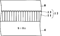
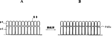
【解決手段】下部電極と、前記下部電極の上に形成され、強誘電体または高誘電率を有する誘電体によって構成される誘電体層と、前記誘電体層の上に形成された上部電極と、を備え、前記下部電極はパラジウムの柱状結晶間にその酸化物である酸化パラジウムを有し、その上層に白金層を具備したことを特徴とする。
【選択図】図1
Description
この誘電体キャパシタは、少なくとも柱状結晶の酸化層であるWOx層、TiOx層、TaOx層、IrO2、PtO2層、RuOx層、ReOx層、PdOx層、OsOx層のいずれか1つの酸化層を有する下部電極、下部電極の上に形成され、強誘電体または高誘電率を有する誘電体によって構成される誘電体層、誘電体層の上に形成された上部電極、を備え、前記酸化層は前記誘電体層からの酸素の抜け出しを防止するように構成されている。
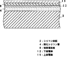
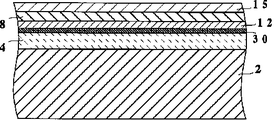
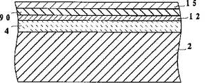
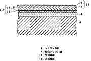
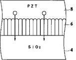
4...酸化シリコン層
8...強誘電体層
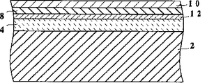
12...下部電極
15...上部電極
90...高誘電率を有する誘電体層
Claims (2)
- 下部電極と、前記下部電極の上に形成され、強誘電体または高誘電率を有する誘電体によって構成される誘電体層と、前記誘電体層の上に形成された上部電極と、を備え、前記下部電極はパラジウムの柱状結晶間にその酸化物である酸化パラジウムを有し、その上層に白金層を具備した誘電体キャパシタ。
- 下部電極を形成するステップと、前記下部電極の上に強誘電体または高誘電率を有する誘電体によって構成される誘電体層を形成するステップと、前記誘電体層の上に上部電極を形成するステップとを備える誘電体キャパシタの製造方法であって、前記下部電極を形成するステップは、柱状結晶構造を有するパラジウムの薄膜を形成する工程と、前記パラジウムの薄膜上に白金の薄膜を形成する工程と、前記パラジウムは酸化する一方前記白金は酸化しない条件の酸化雰囲気中で熱処理を行い、前記パラジウムの薄膜の柱状結晶間のみに酸化パラジウムを形成する工程とからなることを特徴とする誘電体キャパシタの製造方法。
Priority Applications (1)
| Application Number | Priority Date | Filing Date | Title |
|---|---|---|---|
| JP2007011924A JP4255495B2 (ja) | 2007-01-22 | 2007-01-22 | 誘電体キャパシタ |
Applications Claiming Priority (1)
| Application Number | Priority Date | Filing Date | Title |
|---|---|---|---|
| JP2007011924A JP4255495B2 (ja) | 2007-01-22 | 2007-01-22 | 誘電体キャパシタ |
Related Parent Applications (1)
| Application Number | Title | Priority Date | Filing Date |
|---|---|---|---|
| JP17214295A Division JP3929513B2 (ja) | 1995-07-07 | 1995-07-07 | 誘電体キャパシタおよびその製造方法 |
Publications (2)
| Publication Number | Publication Date |
|---|---|
| JP2007158366A true JP2007158366A (ja) | 2007-06-21 |
| JP4255495B2 JP4255495B2 (ja) | 2009-04-15 |
Family
ID=38242205
Family Applications (1)
| Application Number | Title | Priority Date | Filing Date |
|---|---|---|---|
| JP2007011924A Expired - Fee Related JP4255495B2 (ja) | 2007-01-22 | 2007-01-22 | 誘電体キャパシタ |
Country Status (1)
| Country | Link |
|---|---|
| JP (1) | JP4255495B2 (ja) |
-
2007
- 2007-01-22 JP JP2007011924A patent/JP4255495B2/ja not_active Expired - Fee Related
Also Published As
| Publication number | Publication date |
|---|---|
| JP4255495B2 (ja) | 2009-04-15 |
Similar Documents
| Publication | Publication Date | Title |
|---|---|---|
| JP3929513B2 (ja) | 誘電体キャパシタおよびその製造方法 | |
| JP3319994B2 (ja) | 半導体記憶素子 | |
| KR100329533B1 (ko) | 페로브스카이트형산화물막을포함한전자장치와그제조방법및강유전체커패시터 | |
| JP3661850B2 (ja) | 半導体装置およびその製造方法 | |
| JP3461398B2 (ja) | 誘電体キャパシタおよびその製造方法 | |
| JPH07245236A (ja) | 誘電体キャパシタおよびその製造方法 | |
| KR20020016345A (ko) | 강유전체 커패시터를 포함하는 반도체 장치 및 그 제조방법 | |
| JP2004296929A (ja) | 強誘電体キャパシタの製造方法、強誘電体キャパシタ、記憶素子、電子素子、メモリ装置及び電子機器 | |
| JP3810391B2 (ja) | 誘電体キャパシタ | |
| JP4255495B2 (ja) | 誘電体キャパシタ | |
| JP4438963B2 (ja) | 強誘電体キャパシタ | |
| JP2002151654A (ja) | 誘電体キャパシタ素子及びその製造方法 | |
| JP3468706B2 (ja) | 半導体装置およびその製造方法 | |
| JP3954339B2 (ja) | 誘電体キャパシタ | |
| JP3689703B2 (ja) | 誘電体キャパシタおよびその製造方法 | |
| JP3689674B2 (ja) | 誘電体キャパシタおよびその製造方法 | |
| JP3954390B2 (ja) | 誘電体キャパシタ | |
| JP4554631B2 (ja) | 誘電体キャパシタおよびその製造方法 | |
| JP2007184623A (ja) | 誘電体キャパシタ | |
| JP3689702B2 (ja) | 誘電体キャパシタの製造方法 | |
| JP3981142B2 (ja) | 強誘電体キャパシタおよびその製造方法 | |
| JP6217260B2 (ja) | 半導体装置、及び半導体装置の製造方法 | |
| JP3954635B2 (ja) | 誘電体キャパシタの製造方法 | |
| JP2005303324A (ja) | 誘電体キャパシタ | |
| JP2003197772A (ja) | キャパシタ、半導体記憶装置およびその製造方法 |
Legal Events
| Date | Code | Title | Description |
|---|---|---|---|
| RD04 | Notification of resignation of power of attorney |
Free format text: JAPANESE INTERMEDIATE CODE: A7424 Effective date: 20071129 |
|
| TRDD | Decision of grant or rejection written | ||
| A01 | Written decision to grant a patent or to grant a registration (utility model) |
Free format text: JAPANESE INTERMEDIATE CODE: A01 Effective date: 20090120 |
|
| A01 | Written decision to grant a patent or to grant a registration (utility model) |
Free format text: JAPANESE INTERMEDIATE CODE: A01 |
|
| A977 | Report on retrieval |
Free format text: JAPANESE INTERMEDIATE CODE: A971007 Effective date: 20090122 |
|
| A61 | First payment of annual fees (during grant procedure) |
Effective date: 20090127 Free format text: JAPANESE INTERMEDIATE CODE: A61 |
|
| FPAY | Renewal fee payment (prs date is renewal date of database) |
Year of fee payment: 3 Free format text: PAYMENT UNTIL: 20120206 |
|
| R150 | Certificate of patent (=grant) or registration of utility model |
Free format text: JAPANESE INTERMEDIATE CODE: R150 |
|
| FPAY | Renewal fee payment (prs date is renewal date of database) |
Free format text: PAYMENT UNTIL: 20120206 Year of fee payment: 3 |
|
| FPAY | Renewal fee payment (prs date is renewal date of database) |
Free format text: PAYMENT UNTIL: 20130206 Year of fee payment: 4 |
|
| LAPS | Cancellation because of no payment of annual fees |