JP2007123704A - 表面実装型led - Google Patents
表面実装型led Download PDFInfo
- Publication number
- JP2007123704A JP2007123704A JP2005316457A JP2005316457A JP2007123704A JP 2007123704 A JP2007123704 A JP 2007123704A JP 2005316457 A JP2005316457 A JP 2005316457A JP 2005316457 A JP2005316457 A JP 2005316457A JP 2007123704 A JP2007123704 A JP 2007123704A
- Authority
- JP
- Japan
- Prior art keywords
- led
- resin case
- electrode pattern
- polarity
- surface mounting
- Prior art date
- Legal status (The legal status is an assumption and is not a legal conclusion. Google has not performed a legal analysis and makes no representation as to the accuracy of the status listed.)
- Pending
Links
Images


Classifications
-
- H—ELECTRICITY
- H01—ELECTRIC ELEMENTS
- H01L—SEMICONDUCTOR DEVICES NOT COVERED BY CLASS H10
- H01L2224/00—Indexing scheme for arrangements for connecting or disconnecting semiconductor or solid-state bodies and methods related thereto as covered by H01L24/00
- H01L2224/01—Means for bonding being attached to, or being formed on, the surface to be connected, e.g. chip-to-package, die-attach, "first-level" interconnects; Manufacturing methods related thereto
- H01L2224/10—Bump connectors; Manufacturing methods related thereto
- H01L2224/15—Structure, shape, material or disposition of the bump connectors after the connecting process
- H01L2224/16—Structure, shape, material or disposition of the bump connectors after the connecting process of an individual bump connector
-
- H—ELECTRICITY
- H01—ELECTRIC ELEMENTS
- H01L—SEMICONDUCTOR DEVICES NOT COVERED BY CLASS H10
- H01L2224/00—Indexing scheme for arrangements for connecting or disconnecting semiconductor or solid-state bodies and methods related thereto as covered by H01L24/00
- H01L2224/01—Means for bonding being attached to, or being formed on, the surface to be connected, e.g. chip-to-package, die-attach, "first-level" interconnects; Manufacturing methods related thereto
- H01L2224/42—Wire connectors; Manufacturing methods related thereto
- H01L2224/47—Structure, shape, material or disposition of the wire connectors after the connecting process
- H01L2224/48—Structure, shape, material or disposition of the wire connectors after the connecting process of an individual wire connector
- H01L2224/4805—Shape
- H01L2224/4809—Loop shape
- H01L2224/48091—Arched
-
- H—ELECTRICITY
- H01—ELECTRIC ELEMENTS
- H01L—SEMICONDUCTOR DEVICES NOT COVERED BY CLASS H10
- H01L2224/00—Indexing scheme for arrangements for connecting or disconnecting semiconductor or solid-state bodies and methods related thereto as covered by H01L24/00
- H01L2224/93—Batch processes
- H01L2224/95—Batch processes at chip-level, i.e. with connecting carried out on a plurality of singulated devices, i.e. on diced chips
- H01L2224/97—Batch processes at chip-level, i.e. with connecting carried out on a plurality of singulated devices, i.e. on diced chips the devices being connected to a common substrate, e.g. interposer, said common substrate being separable into individual assemblies after connecting
-
- H—ELECTRICITY
- H01—ELECTRIC ELEMENTS
- H01L—SEMICONDUCTOR DEVICES NOT COVERED BY CLASS H10
- H01L2924/00—Indexing scheme for arrangements or methods for connecting or disconnecting semiconductor or solid-state bodies as covered by H01L24/00
- H01L2924/15—Details of package parts other than the semiconductor or other solid state devices to be connected
- H01L2924/181—Encapsulation
Landscapes
- Led Device Packages (AREA)
Abstract
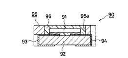
【解決手段】本発明により、回路基板に取付けを行う際に極性マーク7aを基準とする表面実装型LED1において、極性マーク7aは、LEDチップ5を覆う樹脂ケース7の正負側の形状を非対称としてある表面実装型LEDとしたことで、樹脂ケース7が不透明のものになった場合でも、表面実装型LED1の外観から容易に極性が判別できるものとして課題を解決する。
【選択図】図1
Description
2…基板
3…正極パターン3
3a…表正極パターン
3b…裏正極パターン
4…負極パターン
4a…表負極パターン
4b…裏負極パターン
5…LEDチップ
6…金線
7…樹脂ケース
7a…極性マーク
Claims (2)
- 回路基板に取付けを行う際に極性マークを基準とする表面実装型LEDにおいて、前記極性マークは、LEDチップを覆う樹脂ケースの正負側の形状を非対称としてあることを特徴とする表面実装型LED。
- 前記樹脂ケースには蛍光体が混和され、不透明であることを特徴とする請求項1記載の表面実装型LED。
Priority Applications (1)
| Application Number | Priority Date | Filing Date | Title |
|---|---|---|---|
| JP2005316457A JP2007123704A (ja) | 2005-10-31 | 2005-10-31 | 表面実装型led |
Applications Claiming Priority (1)
| Application Number | Priority Date | Filing Date | Title |
|---|---|---|---|
| JP2005316457A JP2007123704A (ja) | 2005-10-31 | 2005-10-31 | 表面実装型led |
Publications (2)
| Publication Number | Publication Date |
|---|---|
| JP2007123704A true JP2007123704A (ja) | 2007-05-17 |
| JP2007123704A5 JP2007123704A5 (ja) | 2008-12-04 |
Family
ID=38147191
Family Applications (1)
| Application Number | Title | Priority Date | Filing Date |
|---|---|---|---|
| JP2005316457A Pending JP2007123704A (ja) | 2005-10-31 | 2005-10-31 | 表面実装型led |
Country Status (1)
| Country | Link |
|---|---|
| JP (1) | JP2007123704A (ja) |
Cited By (6)
| Publication number | Priority date | Publication date | Assignee | Title |
|---|---|---|---|---|
| JP2009152482A (ja) * | 2007-12-21 | 2009-07-09 | Citizen Electronics Co Ltd | 反射枠付表面実装型led |
| JP2012164911A (ja) * | 2011-02-09 | 2012-08-30 | Toshiba Corp | 半導体発光装置 |
| JP2013069765A (ja) * | 2011-09-21 | 2013-04-18 | Citizen Electronics Co Ltd | 半導体発光装置及びその製造方法。 |
| JP2014512559A (ja) * | 2011-02-24 | 2014-05-22 | デジタルオプティクス コーポレーション | カメラモジュールのためのフラッシュシステム |
| WO2016137227A1 (ko) * | 2015-02-24 | 2016-09-01 | 주식회사 세미콘라이트 | 반도체 발광소자 및 이의 제조방법 |
| KR20160103584A (ko) * | 2015-02-24 | 2016-09-02 | 주식회사 세미콘라이트 | 반도체 발광소자, 및 이의 제조방법 |
Citations (3)
| Publication number | Priority date | Publication date | Assignee | Title |
|---|---|---|---|---|
| JPH11330131A (ja) * | 1998-05-20 | 1999-11-30 | Rohm Co Ltd | 半導体装置 |
| JP2000077724A (ja) * | 1998-08-31 | 2000-03-14 | Rohm Co Ltd | 光半導体素子、光半導体素子の実装構造、および光半導体素子群の包装構造 |
| JP2005101283A (ja) * | 2003-09-25 | 2005-04-14 | Matsushita Electric Ind Co Ltd | 表面実装型発光ダイオード |
-
2005
- 2005-10-31 JP JP2005316457A patent/JP2007123704A/ja active Pending
Patent Citations (3)
| Publication number | Priority date | Publication date | Assignee | Title |
|---|---|---|---|---|
| JPH11330131A (ja) * | 1998-05-20 | 1999-11-30 | Rohm Co Ltd | 半導体装置 |
| JP2000077724A (ja) * | 1998-08-31 | 2000-03-14 | Rohm Co Ltd | 光半導体素子、光半導体素子の実装構造、および光半導体素子群の包装構造 |
| JP2005101283A (ja) * | 2003-09-25 | 2005-04-14 | Matsushita Electric Ind Co Ltd | 表面実装型発光ダイオード |
Cited By (10)
| Publication number | Priority date | Publication date | Assignee | Title |
|---|---|---|---|---|
| JP2009152482A (ja) * | 2007-12-21 | 2009-07-09 | Citizen Electronics Co Ltd | 反射枠付表面実装型led |
| JP2012164911A (ja) * | 2011-02-09 | 2012-08-30 | Toshiba Corp | 半導体発光装置 |
| US8860075B2 (en) | 2011-02-09 | 2014-10-14 | Kabushiki Kaisha Toshiba | Semiconductor light emitting device |
| US9263640B2 (en) | 2011-02-09 | 2016-02-16 | Kabushiki Kaisha Toshiba | Semiconductor light emitting device |
| JP2014512559A (ja) * | 2011-02-24 | 2014-05-22 | デジタルオプティクス コーポレーション | カメラモジュールのためのフラッシュシステム |
| JP2013069765A (ja) * | 2011-09-21 | 2013-04-18 | Citizen Electronics Co Ltd | 半導体発光装置及びその製造方法。 |
| US9159887B2 (en) | 2011-09-21 | 2015-10-13 | Citizen Electronics Co., Ltd. | Light-emitting device, lighting device including the light-emitting device, and method of manufacturing the light-emitting device |
| WO2016137227A1 (ko) * | 2015-02-24 | 2016-09-01 | 주식회사 세미콘라이트 | 반도체 발광소자 및 이의 제조방법 |
| KR20160103584A (ko) * | 2015-02-24 | 2016-09-02 | 주식회사 세미콘라이트 | 반도체 발광소자, 및 이의 제조방법 |
| KR101663128B1 (ko) * | 2015-02-24 | 2016-10-10 | 주식회사 세미콘라이트 | 반도체 발광소자, 및 이의 제조방법 |
Similar Documents
| Publication | Publication Date | Title |
|---|---|---|
| US9159887B2 (en) | Light-emitting device, lighting device including the light-emitting device, and method of manufacturing the light-emitting device | |
| JP3741512B2 (ja) | Ledチップ部品 | |
| JP5132404B2 (ja) | 半導体発光装置 | |
| KR20070045462A (ko) | 발광 다이오드 패키지 | |
| JP2007123704A (ja) | 表面実装型led | |
| US8664676B2 (en) | LED package structure housing a LED and a protective zener diode in respective cavities | |
| KR100583162B1 (ko) | 발광 다이오드 패키지 | |
| JP4733434B2 (ja) | チップ型led | |
| JP4989867B2 (ja) | 表面実装型led | |
| JP2012064940A (ja) | 発光ダイオードパッケージ及び発光ダイオード | |
| JPH10150138A (ja) | 下面電極付き側面使用電子部品 | |
| JP4775739B2 (ja) | 照明装置 | |
| JP2008205107A (ja) | 裏面実装型led | |
| JP2007096008A (ja) | 発光素子搭載用パッケージ | |
| JP5099885B2 (ja) | 発光ダイオード | |
| JP2005026619A (ja) | 発光装置 | |
| JP5080843B2 (ja) | 表面実装用スタンド、表面実装型ledランプ及びledユニット | |
| JP2007081219A (ja) | 電子部品 | |
| US20080266826A1 (en) | Assemblable substrate for in-line package and assembly with same | |
| JP4746767B2 (ja) | 発光ダイオード | |
| JP2006332492A (ja) | プリント基板 | |
| JP2006310004A (ja) | 照光式タクトスイッチ | |
| JP2014011444A (ja) | プリント配線板及び発光装置 | |
| JP2006339540A (ja) | チップ型led | |
| JP2007081046A (ja) | 多方向発光ダイオード |
Legal Events
| Date | Code | Title | Description |
|---|---|---|---|
| A521 | Written amendment |
Free format text: JAPANESE INTERMEDIATE CODE: A523 Effective date: 20081020 |
|
| A621 | Written request for application examination |
Free format text: JAPANESE INTERMEDIATE CODE: A621 Effective date: 20081020 |
|
| A977 | Report on retrieval |
Free format text: JAPANESE INTERMEDIATE CODE: A971007 Effective date: 20110322 |
|
| A131 | Notification of reasons for refusal |
Free format text: JAPANESE INTERMEDIATE CODE: A131 Effective date: 20110405 |
|
| A521 | Written amendment |
Free format text: JAPANESE INTERMEDIATE CODE: A523 Effective date: 20110524 |
|
| A02 | Decision of refusal |
Free format text: JAPANESE INTERMEDIATE CODE: A02 Effective date: 20110823 |