JP2007123704A - Surface mounting led - Google Patents
Surface mounting led Download PDFInfo
- Publication number
- JP2007123704A JP2007123704A JP2005316457A JP2005316457A JP2007123704A JP 2007123704 A JP2007123704 A JP 2007123704A JP 2005316457 A JP2005316457 A JP 2005316457A JP 2005316457 A JP2005316457 A JP 2005316457A JP 2007123704 A JP2007123704 A JP 2007123704A
- Authority
- JP
- Japan
- Prior art keywords
- led
- resin case
- electrode pattern
- polarity
- surface mounting
- Prior art date
- Legal status (The legal status is an assumption and is not a legal conclusion. Google has not performed a legal analysis and makes no representation as to the accuracy of the status listed.)
- Pending
Links
Images


Classifications
-
- H—ELECTRICITY
- H01—ELECTRIC ELEMENTS
- H01L—SEMICONDUCTOR DEVICES NOT COVERED BY CLASS H10
- H01L2224/00—Indexing scheme for arrangements for connecting or disconnecting semiconductor or solid-state bodies and methods related thereto as covered by H01L24/00
- H01L2224/01—Means for bonding being attached to, or being formed on, the surface to be connected, e.g. chip-to-package, die-attach, "first-level" interconnects; Manufacturing methods related thereto
- H01L2224/10—Bump connectors; Manufacturing methods related thereto
- H01L2224/15—Structure, shape, material or disposition of the bump connectors after the connecting process
- H01L2224/16—Structure, shape, material or disposition of the bump connectors after the connecting process of an individual bump connector
-
- H—ELECTRICITY
- H01—ELECTRIC ELEMENTS
- H01L—SEMICONDUCTOR DEVICES NOT COVERED BY CLASS H10
- H01L2224/00—Indexing scheme for arrangements for connecting or disconnecting semiconductor or solid-state bodies and methods related thereto as covered by H01L24/00
- H01L2224/01—Means for bonding being attached to, or being formed on, the surface to be connected, e.g. chip-to-package, die-attach, "first-level" interconnects; Manufacturing methods related thereto
- H01L2224/42—Wire connectors; Manufacturing methods related thereto
- H01L2224/47—Structure, shape, material or disposition of the wire connectors after the connecting process
- H01L2224/48—Structure, shape, material or disposition of the wire connectors after the connecting process of an individual wire connector
- H01L2224/4805—Shape
- H01L2224/4809—Loop shape
- H01L2224/48091—Arched
-
- H—ELECTRICITY
- H01—ELECTRIC ELEMENTS
- H01L—SEMICONDUCTOR DEVICES NOT COVERED BY CLASS H10
- H01L2224/00—Indexing scheme for arrangements for connecting or disconnecting semiconductor or solid-state bodies and methods related thereto as covered by H01L24/00
- H01L2224/93—Batch processes
- H01L2224/95—Batch processes at chip-level, i.e. with connecting carried out on a plurality of singulated devices, i.e. on diced chips
- H01L2224/97—Batch processes at chip-level, i.e. with connecting carried out on a plurality of singulated devices, i.e. on diced chips the devices being connected to a common substrate, e.g. interposer, said common substrate being separable into individual assemblies after connecting
-
- H—ELECTRICITY
- H01—ELECTRIC ELEMENTS
- H01L—SEMICONDUCTOR DEVICES NOT COVERED BY CLASS H10
- H01L2924/00—Indexing scheme for arrangements or methods for connecting or disconnecting semiconductor or solid-state bodies as covered by H01L24/00
- H01L2924/15—Details of package parts other than the semiconductor or other solid state devices to be connected
- H01L2924/181—Encapsulation
Landscapes
- Led Device Packages (AREA)
Abstract
Description
本発明は回路基板上にハンダリフローなどにより取付けが行われ、表面実装型と称されている取付け方式のLEDに関するものである。 The present invention relates to a mounting type LED which is mounted on a circuit board by solder reflow or the like and is called a surface mount type.
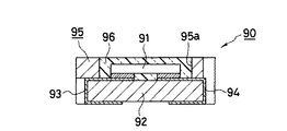
従来の、回路基板に取付けを行う際に、作業者などが極性を明確に判別できる表面実装型LED90の構成としては、図7、図8に示した構成のものがあり、この表面実装型LED90は、LEDチップ91を搭載する基板を形成する際に二枚のグリーンシート92、95を使用する。そして、一方のグリーンシート92には所定のピッチで貫通孔92aが設けられている。
The conventional surface-mounted
また、前記一方のグリーンシート92には、例えば導電性ペイントなどにより、前記貫通孔92aを介して表裏面に到る正電極93と、負電極94とが設けられており、図示で下方の面側に回り込む部分が回路基板(図示は省略する)に取付ける端子部分となり、上方の面側がLEDチップ91を保持する端子部分となる。
In addition, the one
これに対して、他方のグリーンシート95には、一方のグリーンシート92のLEDチップ91が取付けられる部分に対応して、前記LEDチップ91を湿度などから保護するためのエポキシ樹脂などを注入するための、例えば、略長方形とした樹脂注入孔95aが設けられると共に、前記一方のグリーンシート92の設けられた貫通孔92aに対して1個置きとなる位置に同様な貫通孔95bが設けられている。
On the other hand, an epoxy resin or the like for protecting the
以上説明のように形成された一方のグリーンシート92には、図8に示すようにLEDチップ91が取付けられ、必要に応じてワイヤボンドなど内部配線が行われた後には、他方のグリーンシート95と、前記一方のグリーンシート92の貫通孔92aを基準として2枚が重ね合わされ、そして、樹脂注入孔95aへのエポキシ樹脂96の注入などの処理が行われた後に、一方のグリーンシート92の貫通孔92aを基準として、図7中にE−E線で示される位置で切断を行へば、図8に示すように個別のLED90に分割される。
As shown in FIG. 8, the
このようにすることで、分割が行われた1個ごとの表面実装型LED90を上方から見るときには、図8に示すように、一方の端部には半円形の凹部が看視され、これと対峙する他方の端部には凹部は看視されないものとなり、この形状に対して、例えば貫通孔92a、95bが看視できる方が陰極などと、極性を規定しておけば、上面から見た形状を基準として回路基板などへの取付を行えば、例えば、蛍光体の添加により内部構造が外側から見えない表面実装型LED90においても正確な極性として回路基板に取付けることができるものとなる。
しかしながら、近年においては、例えば、携帯電話の個々の数字釦の照明などに使用されるなど、この種の表面実装型LED90の小型化の要求が著しく、現実にも、平面矩形状の表面実装型LED90の長辺側の長さが、約1.0mm程度の小型化されたものまで実用化されている。
However, in recent years, there has been a significant demand for miniaturization of this type of surface-mounted
この場合、上記した従来例のもののように、グリーンシートなどで形成された基台の部分に形状の相違、或いは、マーキングを設けたとしても、基台自体が極小型であり、視認が困難であるばかりでなく、識別用の形状を成形すること自体も困難なものとなってくる。 In this case, as in the conventional example described above, even if a difference in shape or marking is provided on the base portion formed of a green sheet or the like, the base itself is extremely small and difficult to see. Not only is it difficult to form a shape for identification itself.
また、グリーンシート92などの適宜な位置に塗料などで極性マークを印刷するなどの手段も行われているが、上記したように、近年では、青色発光のLEDチップからの光で黄色発光を行う蛍光体と組合わせることで、白色の光を得る表面実装型LED90が、バックライト照明用などとして、多用されるようになり、この場合には、前記エポキシ樹脂96に蛍光体が添加されるものとなり、不透明となって極性マークが遮蔽され、外部からの目視では正負極の確認が、ますます困難となっているのが実情である。
In addition, a means such as printing a polar mark with a paint or the like at an appropriate position such as the
よって、現状では、最も面積のとれる基板の裏面などに印刷など適宜な手段で極性マークを設けざるを得ないものとなり、表面実装型LED90の回路基板への取付の際には、裏返しては極性を確認するなど、製造時の工程が繁雑化はしてコストアップの要因と成る。
Therefore, at present, the polarity mark has to be provided by an appropriate means such as printing on the back surface of the substrate having the largest area. When mounting the surface
特に近年においては、上記、携帯電話の普及などによりこの種の表面実装型LED90に対しては、ますます小型化が要求されると共に、発光色も。表示のフルカラー化などにより、LED側も、ほとんどのものが白色のものが要求され、上記した各問題点は一層にこの種の表面実装型LED90の組立作業上の問題点となっている。
Particularly in recent years, due to the spread of mobile phones and the like, this type of surface-mounted
本発明は、上記した課題を解決するための具体的手段として、回路基板に取付けを行う際に極性マークを基準とする表面実装型LEDにおいて、前記極性マークは、LEDチップを覆う樹脂ケースの正負側の形状を非対称としてあることを特徴とする表面実装型LEDを提供することで課題を解決するものである。 As a specific means for solving the above-described problems, the present invention provides a surface mount type LED that uses a polarity mark as a reference when mounting on a circuit board. The polarity mark is a sign of a resin case that covers the LED chip. The problem is solved by providing a surface-mounted LED characterized in that the shape on the side is asymmetric.
本発明により、表面実装型LEDにおいて、回路基板に取付けるときの、正負極性表示マークとして、樹脂ケースの形状を正負が非対称とすることで、例えば、樹脂ケースが不透明の場合であっても、明確に判断が行えるものとして、誤組立を予防し、また、製品検査時にも、誤組立が行われたものの発見を容易として、もって、製品の品質向上を可能とするという優れた効果を奏する。 According to the present invention, in a surface mount type LED, as a positive / negative polarity display mark when attached to a circuit board, the shape of the resin case is made asymmetrical between positive and negative, for example, even when the resin case is opaque Therefore, it is possible to prevent misassembly, and at the time of product inspection, it is easy to find what has been misassembled, so that it is possible to improve the quality of the product.
つぎに、本発明を図に示す実施形態に基づいて詳細に説明する。図1に符号1で示すものは本発明に係る表面実装型LEDの第一実施形態であり、この表面実装型LED1の、例えば長方形とした基板2の表面側には、長辺側で対峙するようにして一方の端部には正極パターン3が設けられ、他の一方の端部には負極パターン4が設けられている。
Below, this invention is demonstrated in detail based on embodiment shown in a figure. 1 is a first embodiment of the surface-mounted LED according to the present invention, and the surface side of the surface-mounted LED 1, for example, a
そして、前記基板2の前記正極パターン3の表面側の表正極パターン3aに対応しては、裏正極パターン3bが敷設され、負極パターン4の表負極パターン4aに対応しては裏負極パターン4bが敷設されている。そして、表正極パターン3aと、裏正極パターン3bは、基板2の板厚面に施された無電界メッキなどにより電気的に接続され、同様に、表負極パターン4aと裏負極パターン4bも電気的に接続されている。
A back
また、前記基板2の表面側においては、表負極パターン4a上にLEDチップ5がダイボンドされ、金線6などで表正極パターン3aと接続され、更にエポキシ樹脂などによる樹脂ケース7がトランスファモールド、ポッティングモールドなど適宜な方法で形成され、前記LEDチップ5、及び、金線6を覆い、湿度、外部応力などから保護している。尚、このときに、本発明においては、前記樹脂ケース7は透明のものでも良く、或いは、蛍光体が添加されて不透明のものであっても良い。
On the surface side of the
ここで、本発明においては、前記樹脂ケース7を形成するときの金型に工夫を凝らすものであり、例えば、図1に示すように、例えば負極側の面の角を面取りを行い、これをもって極性マーク7aとする。よって、樹脂ケース7は透明、不透明の別なく極性マーク7aが明確に表示されるものとなり、誤組立を防止できるものとなる。
Here, in the present invention, the mold for forming the
また、本発明により極性マーク7aを上記の形状としたことで、視覚のみでなく触覚でも極性マーク7aの位置が判別できるものとなるので、作業者がある程度も経験を積めば、視覚に頼ることなく、触覚のみでプリント回路基板への搭載が可能となる、或いは産業ロボットでプリント回路基板へ搭載するときの精度を向上できるなども作用、効果も期待できるものとなる。
In addition, since the
尚、本発明においては、前記極性マーク7aは、上記に説明したように樹脂ケース7の負極パターン4aの上辺を面取りした形状に限定するものではなく、図2に第二実施形態として示すようにコーナー部分を切落としたような形状であっても良い。要は樹脂ケース7側から見て極性マーク7aが認識できればよいものである。
In the present invention, the
更には、以上の例は、樹脂ケース7が基本的には立方体形状、或いは、直方体形状の一部を切り取った形状であったが、本発明では、これをも限定するものではなく、図3〜図6に第三〜第六実施形態として示すように樹脂ケース7自体の陰極側の形状を、略台形状(第三実施形態)、略三角状(第四実施形態)、略隅切り状(第五実施形態)、略円弧状(第六実施形態)などに変形させても良いものである。
Further, in the above example, the
ここで、本発明によれば、基板2の形状、及び、製法は旧来から行われているものと全く代わることがなく、また、樹脂ケース7においても金型の形状が変わるのみで、構成、及び、工程が変わるものではない。従って、信頼性などに全く影響を生じることなく、工程の煩雑化によるコストアップも一切に生じることはない。
Here, according to the present invention, the shape of the
1…表面実装型LED
2…基板
3…正極パターン3
3a…表正極パターン
3b…裏正極パターン
4…負極パターン
4a…表負極パターン
4b…裏負極パターン
5…LEDチップ
6…金線
7…樹脂ケース
7a…極性マーク
1… Surface mount LED
2 ...
3a ... Front
Claims (2)
Priority Applications (1)
| Application Number | Priority Date | Filing Date | Title |
|---|---|---|---|
| JP2005316457A JP2007123704A (en) | 2005-10-31 | 2005-10-31 | Surface mounting led |
Applications Claiming Priority (1)
| Application Number | Priority Date | Filing Date | Title |
|---|---|---|---|
| JP2005316457A JP2007123704A (en) | 2005-10-31 | 2005-10-31 | Surface mounting led |
Publications (2)
| Publication Number | Publication Date |
|---|---|
| JP2007123704A true JP2007123704A (en) | 2007-05-17 |
| JP2007123704A5 JP2007123704A5 (en) | 2008-12-04 |
Family
ID=38147191
Family Applications (1)
| Application Number | Title | Priority Date | Filing Date |
|---|---|---|---|
| JP2005316457A Pending JP2007123704A (en) | 2005-10-31 | 2005-10-31 | Surface mounting led |
Country Status (1)
| Country | Link |
|---|---|
| JP (1) | JP2007123704A (en) |
Cited By (6)
| Publication number | Priority date | Publication date | Assignee | Title |
|---|---|---|---|---|
| JP2009152482A (en) * | 2007-12-21 | 2009-07-09 | Citizen Electronics Co Ltd | Surface mounting led with reflection frame |
| JP2012164911A (en) * | 2011-02-09 | 2012-08-30 | Toshiba Corp | Semiconductor light-emitting device |
| JP2013069765A (en) * | 2011-09-21 | 2013-04-18 | Citizen Electronics Co Ltd | Semiconductor light-emitting device and manufacturing method of the same |
| JP2014512559A (en) * | 2011-02-24 | 2014-05-22 | デジタルオプティクス コーポレーション | Flash system for camera module |
| WO2016137227A1 (en) * | 2015-02-24 | 2016-09-01 | 주식회사 세미콘라이트 | Semiconductor light emitting device and manufacturing method therefor |
| KR20160103584A (en) * | 2015-02-24 | 2016-09-02 | 주식회사 세미콘라이트 | Semiconductor light emitting device and method of manufacturing the same |
Citations (3)
| Publication number | Priority date | Publication date | Assignee | Title |
|---|---|---|---|---|
| JPH11330131A (en) * | 1998-05-20 | 1999-11-30 | Rohm Co Ltd | Semiconductor device |
| JP2000077724A (en) * | 1998-08-31 | 2000-03-14 | Rohm Co Ltd | Optical semiconductor element, packaging structure thereof and packaging structure of group thereof |
| JP2005101283A (en) * | 2003-09-25 | 2005-04-14 | Matsushita Electric Ind Co Ltd | Surface-mounted light emitting diode |
-
2005
- 2005-10-31 JP JP2005316457A patent/JP2007123704A/en active Pending
Patent Citations (3)
| Publication number | Priority date | Publication date | Assignee | Title |
|---|---|---|---|---|
| JPH11330131A (en) * | 1998-05-20 | 1999-11-30 | Rohm Co Ltd | Semiconductor device |
| JP2000077724A (en) * | 1998-08-31 | 2000-03-14 | Rohm Co Ltd | Optical semiconductor element, packaging structure thereof and packaging structure of group thereof |
| JP2005101283A (en) * | 2003-09-25 | 2005-04-14 | Matsushita Electric Ind Co Ltd | Surface-mounted light emitting diode |
Cited By (10)
| Publication number | Priority date | Publication date | Assignee | Title |
|---|---|---|---|---|
| JP2009152482A (en) * | 2007-12-21 | 2009-07-09 | Citizen Electronics Co Ltd | Surface mounting led with reflection frame |
| JP2012164911A (en) * | 2011-02-09 | 2012-08-30 | Toshiba Corp | Semiconductor light-emitting device |
| US8860075B2 (en) | 2011-02-09 | 2014-10-14 | Kabushiki Kaisha Toshiba | Semiconductor light emitting device |
| US9263640B2 (en) | 2011-02-09 | 2016-02-16 | Kabushiki Kaisha Toshiba | Semiconductor light emitting device |
| JP2014512559A (en) * | 2011-02-24 | 2014-05-22 | デジタルオプティクス コーポレーション | Flash system for camera module |
| JP2013069765A (en) * | 2011-09-21 | 2013-04-18 | Citizen Electronics Co Ltd | Semiconductor light-emitting device and manufacturing method of the same |
| US9159887B2 (en) | 2011-09-21 | 2015-10-13 | Citizen Electronics Co., Ltd. | Light-emitting device, lighting device including the light-emitting device, and method of manufacturing the light-emitting device |
| WO2016137227A1 (en) * | 2015-02-24 | 2016-09-01 | 주식회사 세미콘라이트 | Semiconductor light emitting device and manufacturing method therefor |
| KR20160103584A (en) * | 2015-02-24 | 2016-09-02 | 주식회사 세미콘라이트 | Semiconductor light emitting device and method of manufacturing the same |
| KR101663128B1 (en) * | 2015-02-24 | 2016-10-10 | 주식회사 세미콘라이트 | Semiconductor light emitting device and method of manufacturing the same |
Similar Documents
| Publication | Publication Date | Title |
|---|---|---|
| US9159887B2 (en) | Light-emitting device, lighting device including the light-emitting device, and method of manufacturing the light-emitting device | |
| JP3741512B2 (en) | LED chip parts | |
| KR20070045462A (en) | Package of light emitting diode | |
| JP2007123704A (en) | Surface mounting led | |
| US8664676B2 (en) | LED package structure housing a LED and a protective zener diode in respective cavities | |
| KR100583162B1 (en) | Light emitting diode package | |
| CN110993777B (en) | Display driving board, preparation method thereof and display device | |
| JP4733434B2 (en) | Chip type LED | |
| JP4989867B2 (en) | Surface mount type LED | |
| JP2012064940A (en) | Light emitting diode package and light emitting diode | |
| JPH10150138A (en) | Side-use electronic component provided with lower electrode | |
| JP4775739B2 (en) | Lighting device | |
| JP2008205107A (en) | Back mounting led | |
| JP2007096008A (en) | Package for mounting light emitting element | |
| JP5099885B2 (en) | Light emitting diode | |
| JP2005026619A (en) | Light emitting device | |
| JP5080843B2 (en) | Surface mount stand, surface mount LED lamp and LED unit | |
| JP2007081219A (en) | Electronic component | |
| US20080266826A1 (en) | Assemblable substrate for in-line package and assembly with same | |
| JP4746767B2 (en) | Light emitting diode | |
| JP2006332492A (en) | Printed-circuit board | |
| JP2006310004A (en) | Illuminated tactile switch | |
| JP2014011444A (en) | Printed board and light-emitting device | |
| JP2006339540A (en) | Chip led | |
| JP2007081046A (en) | Multi-directional light emitting diode |
Legal Events
| Date | Code | Title | Description |
|---|---|---|---|
| A521 | Written amendment |
Free format text: JAPANESE INTERMEDIATE CODE: A523 Effective date: 20081020 |
|
| A621 | Written request for application examination |
Free format text: JAPANESE INTERMEDIATE CODE: A621 Effective date: 20081020 |
|
| A977 | Report on retrieval |
Free format text: JAPANESE INTERMEDIATE CODE: A971007 Effective date: 20110322 |
|
| A131 | Notification of reasons for refusal |
Free format text: JAPANESE INTERMEDIATE CODE: A131 Effective date: 20110405 |
|
| A521 | Written amendment |
Free format text: JAPANESE INTERMEDIATE CODE: A523 Effective date: 20110524 |
|
| A02 | Decision of refusal |
Free format text: JAPANESE INTERMEDIATE CODE: A02 Effective date: 20110823 |