JP2005524994A - 高結合比浮遊ゲートメモリセル - Google Patents
高結合比浮遊ゲートメモリセル Download PDFInfo
- Publication number
- JP2005524994A JP2005524994A JP2004504303A JP2004504303A JP2005524994A JP 2005524994 A JP2005524994 A JP 2005524994A JP 2004504303 A JP2004504303 A JP 2004504303A JP 2004504303 A JP2004504303 A JP 2004504303A JP 2005524994 A JP2005524994 A JP 2005524994A
- Authority
- JP
- Japan
- Prior art keywords
- conductive
- layer
- control gate
- spacer
- memory device
- Prior art date
- Legal status (The legal status is an assumption and is not a legal conclusion. Google has not performed a legal analysis and makes no representation as to the accuracy of the status listed.)
- Pending
Links
- 238000007667 floating Methods 0.000 title claims abstract description 35
- 230000008878 coupling Effects 0.000 title claims abstract description 20
- 238000010168 coupling process Methods 0.000 title claims abstract description 20
- 238000005859 coupling reaction Methods 0.000 title claims abstract description 20
- 125000006850 spacer group Chemical group 0.000 claims abstract description 95
- 238000000034 method Methods 0.000 claims abstract description 37
- 239000004065 semiconductor Substances 0.000 claims abstract description 35
- 229910021420 polycrystalline silicon Inorganic materials 0.000 claims description 29
- 229920005591 polysilicon Polymers 0.000 claims description 29
- 239000000758 substrate Substances 0.000 claims description 26
- 238000000151 deposition Methods 0.000 claims description 8
- 238000005530 etching Methods 0.000 claims description 7
- 230000015572 biosynthetic process Effects 0.000 claims description 4
- 238000004519 manufacturing process Methods 0.000 claims description 4
- 229910021332 silicide Inorganic materials 0.000 claims description 3
- FVBUAEGBCNSCDD-UHFFFAOYSA-N silicide(4-) Chemical group [Si-4] FVBUAEGBCNSCDD-UHFFFAOYSA-N 0.000 claims description 3
- 230000008021 deposition Effects 0.000 claims 2
- 230000008569 process Effects 0.000 description 15
- VYPSYNLAJGMNEJ-UHFFFAOYSA-N Silicium dioxide Chemical compound O=[Si]=O VYPSYNLAJGMNEJ-UHFFFAOYSA-N 0.000 description 8
- XUIMIQQOPSSXEZ-UHFFFAOYSA-N Silicon Chemical compound [Si] XUIMIQQOPSSXEZ-UHFFFAOYSA-N 0.000 description 6
- 229910052710 silicon Inorganic materials 0.000 description 6
- 239000010703 silicon Substances 0.000 description 6
- 238000002513 implantation Methods 0.000 description 5
- 239000000463 material Substances 0.000 description 5
- XYFCBTPGUUZFHI-UHFFFAOYSA-N Phosphine Chemical compound P XYFCBTPGUUZFHI-UHFFFAOYSA-N 0.000 description 4
- 239000003989 dielectric material Substances 0.000 description 4
- 230000008901 benefit Effects 0.000 description 3
- 238000002347 injection Methods 0.000 description 3
- 239000007924 injection Substances 0.000 description 3
- 150000004767 nitrides Chemical class 0.000 description 3
- 230000002093 peripheral effect Effects 0.000 description 3
- 238000012545 processing Methods 0.000 description 3
- 235000012239 silicon dioxide Nutrition 0.000 description 3
- 239000000377 silicon dioxide Substances 0.000 description 3
- JBRZTFJDHDCESZ-UHFFFAOYSA-N AsGa Chemical compound [As]#[Ga] JBRZTFJDHDCESZ-UHFFFAOYSA-N 0.000 description 2
- BLRPTPMANUNPDV-UHFFFAOYSA-N Silane Chemical compound [SiH4] BLRPTPMANUNPDV-UHFFFAOYSA-N 0.000 description 2
- 229910000577 Silicon-germanium Inorganic materials 0.000 description 2
- BOTDANWDWHJENH-UHFFFAOYSA-N Tetraethyl orthosilicate Chemical compound CCO[Si](OCC)(OCC)OCC BOTDANWDWHJENH-UHFFFAOYSA-N 0.000 description 2
- RBFQJDQYXXHULB-UHFFFAOYSA-N arsane Chemical compound [AsH3] RBFQJDQYXXHULB-UHFFFAOYSA-N 0.000 description 2
- 229910052785 arsenic Inorganic materials 0.000 description 2
- RQNWIZPPADIBDY-UHFFFAOYSA-N arsenic atom Chemical compound [As] RQNWIZPPADIBDY-UHFFFAOYSA-N 0.000 description 2
- 230000007423 decrease Effects 0.000 description 2
- 238000005137 deposition process Methods 0.000 description 2
- 239000011521 glass Substances 0.000 description 2
- 239000007943 implant Substances 0.000 description 2
- 239000012535 impurity Substances 0.000 description 2
- 238000004518 low pressure chemical vapour deposition Methods 0.000 description 2
- 230000000873 masking effect Effects 0.000 description 2
- 230000007246 mechanism Effects 0.000 description 2
- -1 phosphorous ions Chemical class 0.000 description 2
- 229910052698 phosphorus Inorganic materials 0.000 description 2
- 239000011574 phosphorus Substances 0.000 description 2
- 229910000073 phosphorus hydride Inorganic materials 0.000 description 2
- 229910000077 silane Inorganic materials 0.000 description 2
- 229910052814 silicon oxide Inorganic materials 0.000 description 2
- 230000005689 Fowler Nordheim tunneling Effects 0.000 description 1
- 229910001218 Gallium arsenide Inorganic materials 0.000 description 1
- OAICVXFJPJFONN-UHFFFAOYSA-N Phosphorus Chemical compound [P] OAICVXFJPJFONN-UHFFFAOYSA-N 0.000 description 1
- 229910052581 Si3N4 Inorganic materials 0.000 description 1
- 229910004298 SiO 2 Inorganic materials 0.000 description 1
- LEVVHYCKPQWKOP-UHFFFAOYSA-N [Si].[Ge] Chemical compound [Si].[Ge] LEVVHYCKPQWKOP-UHFFFAOYSA-N 0.000 description 1
- QVGXLLKOCUKJST-UHFFFAOYSA-N atomic oxygen Chemical compound [O] QVGXLLKOCUKJST-UHFFFAOYSA-N 0.000 description 1
- 230000004888 barrier function Effects 0.000 description 1
- 238000004364 calculation method Methods 0.000 description 1
- 230000008859 change Effects 0.000 description 1
- 239000004020 conductor Substances 0.000 description 1
- 238000007796 conventional method Methods 0.000 description 1
- 230000003247 decreasing effect Effects 0.000 description 1
- 239000002019 doping agent Substances 0.000 description 1
- 230000005684 electric field Effects 0.000 description 1
- 238000005516 engineering process Methods 0.000 description 1
- 230000006870 function Effects 0.000 description 1
- 229910052732 germanium Inorganic materials 0.000 description 1
- GNPVGFCGXDBREM-UHFFFAOYSA-N germanium atom Chemical compound [Ge] GNPVGFCGXDBREM-UHFFFAOYSA-N 0.000 description 1
- 239000011810 insulating material Substances 0.000 description 1
- 238000009413 insulation Methods 0.000 description 1
- 238000005468 ion implantation Methods 0.000 description 1
- 150000002500 ions Chemical class 0.000 description 1
- 238000002955 isolation Methods 0.000 description 1
- 229910052751 metal Inorganic materials 0.000 description 1
- 239000002184 metal Substances 0.000 description 1
- 239000000203 mixture Substances 0.000 description 1
- 230000004048 modification Effects 0.000 description 1
- 238000012986 modification Methods 0.000 description 1
- 230000003647 oxidation Effects 0.000 description 1
- 238000007254 oxidation reaction Methods 0.000 description 1
- 229910052760 oxygen Inorganic materials 0.000 description 1
- 239000001301 oxygen Substances 0.000 description 1
- 238000000623 plasma-assisted chemical vapour deposition Methods 0.000 description 1
- 238000012805 post-processing Methods 0.000 description 1
- 229910052594 sapphire Inorganic materials 0.000 description 1
- 239000010980 sapphire Substances 0.000 description 1
- HQVNEWCFYHHQES-UHFFFAOYSA-N silicon nitride Chemical compound N12[Si]34N5[Si]62N3[Si]51N64 HQVNEWCFYHHQES-UHFFFAOYSA-N 0.000 description 1
- 230000000153 supplemental effect Effects 0.000 description 1
- 230000005641 tunneling Effects 0.000 description 1
Images


Classifications
-
- H—ELECTRICITY
- H01—ELECTRIC ELEMENTS
- H01L—SEMICONDUCTOR DEVICES NOT COVERED BY CLASS H10
- H01L29/00—Semiconductor devices adapted for rectifying, amplifying, oscillating or switching, or capacitors or resistors with at least one potential-jump barrier or surface barrier, e.g. PN junction depletion layer or carrier concentration layer; Details of semiconductor bodies or of electrodes thereof ; Multistep manufacturing processes therefor
- H01L29/66—Types of semiconductor device ; Multistep manufacturing processes therefor
- H01L29/68—Types of semiconductor device ; Multistep manufacturing processes therefor controllable by only the electric current supplied, or only the electric potential applied, to an electrode which does not carry the current to be rectified, amplified or switched
- H01L29/76—Unipolar devices, e.g. field effect transistors
- H01L29/772—Field effect transistors
- H01L29/78—Field effect transistors with field effect produced by an insulated gate
- H01L29/788—Field effect transistors with field effect produced by an insulated gate with floating gate
- H01L29/7881—Programmable transistors with only two possible levels of programmation
-
- H—ELECTRICITY
- H01—ELECTRIC ELEMENTS
- H01L—SEMICONDUCTOR DEVICES NOT COVERED BY CLASS H10
- H01L29/00—Semiconductor devices adapted for rectifying, amplifying, oscillating or switching, or capacitors or resistors with at least one potential-jump barrier or surface barrier, e.g. PN junction depletion layer or carrier concentration layer; Details of semiconductor bodies or of electrodes thereof ; Multistep manufacturing processes therefor
- H01L29/40—Electrodes ; Multistep manufacturing processes therefor
- H01L29/41—Electrodes ; Multistep manufacturing processes therefor characterised by their shape, relative sizes or dispositions
- H01L29/423—Electrodes ; Multistep manufacturing processes therefor characterised by their shape, relative sizes or dispositions not carrying the current to be rectified, amplified or switched
- H01L29/42312—Gate electrodes for field effect devices
- H01L29/42316—Gate electrodes for field effect devices for field-effect transistors
- H01L29/4232—Gate electrodes for field effect devices for field-effect transistors with insulated gate
- H01L29/42324—Gate electrodes for transistors with a floating gate
Abstract
Description
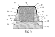
平坦な表面を有する基板と、
前記基板上に浮遊ゲートと制御ゲートとを備え、前記平坦な表面に対してほぼ垂直に延びる二つの対向する壁を有するスタックと、
前記スタックの各対向壁と関わる導電スペーサと、
前記スタックの各対向壁と前記関わる導電スペーサとの間に絶縁層と、
各導電スペーサと前記制御ゲートとの間にガルバニック・コンタクトとを備えた半導体メモリ装置を提供する。
浮遊ゲートと制御ゲートとを前記基板上に備え、前記平坦な表面に対してほぼ垂直に延びる二つの対向する壁を有するスタックを形成する工程と、
前記スタックの各対向壁と関わる導電スペーサを形成する工程と、
前記スタックの各対向壁と前記関わる導電スペーサとの間に絶縁層を形成する工程と、
各導電スペーサと前記制御ゲートとの間にガルバニック・コンタクトを形成する工程とを備える。
L = 150 nm (トランジスタ長さ)
W = 160 nm (トランジスタ幅)
K = 320 nm (浮遊ゲート幅)
tox = 8.5 nm (トンネル酸化物厚み)
tipd = 15 nm (IPD等価電気的厚み)
h = 150 nm (浮遊ゲート厚み)
導電スペーサを有しない従来の装置では次のように結合比αcgが得られる。
= εoεrAok /tox = 9.75 x 10⁻¹⁷F
Aipd = W x (2h + K) = 9.92 x 10⁻¹⁴m2 ⇒ Cipd
= εoεrAipd /tipd = 2.28 x 10⁻¹⁶F
αcg = Cipd/(Cipd /+ Cox) = 0.69
導電スペーサを有するこの発明の装置では次のように結合比αcgが得られる。
Aipd が大きくなるのでCipdも大きくなる:
Aipd = W x (2h + K) + (2h + K) = 1.95 x 10⁻¹³m2 ⇒ Cipd = 4.49 x 10⁻¹⁶F
αcg = Cipd/(Cipd /+ Cox) = 0.82
これは、この例では、結合比が19%上昇したこと、又は、つまり書き込み及び消去に必要な電圧が約20%下げられることを意味する。
Claims (25)
- 浮遊ゲートと制御ゲートの結合比を制御する不揮発性浮遊ゲート半導体メモリ装置であって、
平坦な表面を有する基板と、
前記基板上に浮遊ゲートと制御ゲートとを備え、前記平坦な表面に対してほぼ垂直に延びる二つの対向する壁を有するスタックと、
前記スタックの各対向壁と関わる導電スペーサと、
前記スタックの各対向壁と前記関わる導電スペーサとの間に絶縁層と、
各導電スペーサと前記制御ゲートとの間にガルバニック・コンタクトとを備えた半導体メモリ装置。 - 前記スタックはさらに誘電体層を備えたことを特徴とする請求項1に記載の半導体メモリ装置。
- 前記絶縁層は前記誘電体層と同じオーダの電気的な厚みを有することを特徴とする請求項2に記載の半導体メモリ装置。
- 前記絶縁層はブランケット層を用いて形成されることを特徴とする請求項1に記載の半導体メモリ装置。
- 前記絶縁層はスペーサを用いて形成されることを特徴とする請求項1に記載の半導体メモリ装置。
- 前記ガルバニック・コンタクトは各導電スペーサと前記制御ゲートとの間の直接接触により形成されることを特徴とする請求項5に記載の半導体メモリ装置。
- 前記複数導電スペーサと前記制御ゲートとの間の前記ガルバニック・コンタクトは、少なくとも前記導電スペーサの一部と少なくとも前記制御ゲートの一部との上部の導電層を用いて形成されることを特徴とする請求項1に記載の半導体メモリ装置。
- 前記導電層はシリサイド層であることを特徴とする請求項7に記載の半導体メモリ装置。
- 前記導電スペーサはポリシリコンを備えたことを特徴とする請求項1に記載の半導体メモリ装置。
- ソース及びドレイン領域をさらに備えたことを特徴とする請求項1に記載の半導体メモリ装置。
- 前記複数導電スペーサに沿って複数絶縁スペーサをさらに備えたことを特徴とする請求項1に記載の半導体メモリ装置。
- 平坦な表面を有する基板上に、浮遊ゲートと制御ゲートの結合比を有する不揮発性浮遊ゲート半導体メモリ装置を製造する方法であって、
浮遊ゲートと制御ゲートとを前記基板上に備え、前記平坦な表面に対してほぼ垂直に延びる二つの対向する壁を有するスタックを形成する工程と、
前記スタックの各対向壁と関わる導電スペーサを形成する工程と、
前記スタックの各対向壁と前記関わる導電スペーサとの間に絶縁層を形成する工程と、
各導電スペーサと前記制御ゲートとの間にガルバニック・コンタクトを形成する工程とを備えた方法。 - 前記絶縁層形成工程はブランケット層を堆積する工程を備えたことを特徴とする請求項12に記載の方法。
- 前記絶縁層形成工程は複数絶縁スペーサを形成する工程を備えたことを特徴とする請求項12に記載の方法。
- 前記ガルバニック・コンタクト形成工程は各導電スペーサと前記制御ゲートとの間を直接接触させる工程を備えたことを特徴とする請求項14に記載の方法。
- 各導電スペーサと前記制御ゲートとの間にガルバニック結合を形成する工程は、少なくとも前記制御ゲートの一部と少なくとも前記複数導電スペーサの一部との上部に導電層を形成する工程を備えたことを特徴とする請求項12に記載の方法。
- 前記制御ゲートと前記複数導電スペーサはシリサイド化されることを特徴とする請求項16に記載の方法。
- 前記複数導電スペーサ形成工程は、導電層を堆積し、そして該導電層を異方性エッチングする工程を備えたことを特徴とする請求項12に記載の方法。
- 前記スタック形成工程は、
浮遊ゲート層を堆積する工程と、
制御ゲート層を堆積する工程と、
前記スタックをエッチングする工程とを備えたことを特徴とする請求項12に記載の方法。 - 前記浮遊ゲート層堆積工程と前記制御ゲート層堆積工程との間に誘電体層を堆積する工程をさらに備えたことを特徴とする請求項19に記載の方法。
- ソース及びドレイン領域を設ける工程をさらに備えたことを特徴とする請求項12に記載の方法。
- 前記複数導電スペーサに沿って複数絶縁スペーサを設ける工程をさらに備えたことを特徴とする請求項12記載の方法。
- 請求項1乃至11記載の半導体装置を含むことを特徴とする不揮発性メモリ。
- 前記メモリはフラッシュメモリであることを特徴とする請求項23記載の不揮発性メモリ。
- 前記メモリはEEPROMであることを特徴とする請求項23記載の不揮発性メモリ。
Applications Claiming Priority (2)
| Application Number | Priority Date | Filing Date | Title |
|---|---|---|---|
| EP02076771 | 2002-05-08 | ||
| PCT/IB2003/001485 WO2003096431A1 (en) | 2002-05-08 | 2003-04-11 | Floating gate memory cells with increased coupling ratio |
Publications (2)
| Publication Number | Publication Date |
|---|---|
| JP2005524994A true JP2005524994A (ja) | 2005-08-18 |
| JP2005524994A5 JP2005524994A5 (ja) | 2006-06-01 |
Family
ID=29414749
Family Applications (1)
| Application Number | Title | Priority Date | Filing Date |
|---|---|---|---|
| JP2004504303A Pending JP2005524994A (ja) | 2002-05-08 | 2003-04-11 | 高結合比浮遊ゲートメモリセル |
Country Status (9)
| Country | Link |
|---|---|
| US (1) | US7045852B2 (ja) |
| EP (1) | EP1506580B1 (ja) |
| JP (1) | JP2005524994A (ja) |
| CN (1) | CN100533772C (ja) |
| AT (1) | ATE475200T1 (ja) |
| AU (1) | AU2003216649A1 (ja) |
| DE (1) | DE60333452D1 (ja) |
| TW (1) | TWI306312B (ja) |
| WO (1) | WO2003096431A1 (ja) |
Cited By (1)
| Publication number | Priority date | Publication date | Assignee | Title |
|---|---|---|---|---|
| JP2009278098A (ja) * | 2008-05-13 | 2009-11-26 | Hynix Semiconductor Inc | フラッシュメモリ素子及びその製造方法 |
Families Citing this family (19)
| Publication number | Priority date | Publication date | Assignee | Title |
|---|---|---|---|---|
| US7221008B2 (en) * | 2003-10-06 | 2007-05-22 | Sandisk Corporation | Bitline direction shielding to avoid cross coupling between adjacent cells for NAND flash memory |
| KR100650369B1 (ko) * | 2004-10-01 | 2006-11-27 | 주식회사 하이닉스반도체 | 폴리실리콘부유측벽을 갖는 비휘발성메모리장치 및 그제조 방법 |
| US7381615B2 (en) * | 2004-11-23 | 2008-06-03 | Sandisk Corporation | Methods for self-aligned trench filling with grown dielectric for high coupling ratio in semiconductor devices |
| US7416956B2 (en) * | 2004-11-23 | 2008-08-26 | Sandisk Corporation | Self-aligned trench filling for narrow gap isolation regions |
| US7319618B2 (en) * | 2005-08-16 | 2008-01-15 | Macronic International Co., Ltd. | Low-k spacer structure for flash memory |
| US7541241B2 (en) * | 2005-12-12 | 2009-06-02 | Promos Technologies, Inc. | Method for fabricating memory cell |
| JP4364225B2 (ja) * | 2006-09-15 | 2009-11-11 | 株式会社東芝 | 半導体装置およびその製造方法 |
| US8325530B2 (en) * | 2006-10-03 | 2012-12-04 | Macronix International Co., Ltd. | Cell operation methods using gate-injection for floating gate NAND flash memory |
| US20080157169A1 (en) * | 2006-12-28 | 2008-07-03 | Yuan Jack H | Shield plates for reduced field coupling in nonvolatile memory |
| US20080160680A1 (en) * | 2006-12-28 | 2008-07-03 | Yuan Jack H | Methods of fabricating shield plates for reduced field coupling in nonvolatile memory |
| TW200847404A (en) * | 2007-05-18 | 2008-12-01 | Nanya Technology Corp | Flash memory device and method for fabricating thereof |
| CN101866691B (zh) * | 2010-04-29 | 2015-06-17 | 上海华虹宏力半导体制造有限公司 | 获得快闪存储单元电容耦合率的方法 |
| CN102867748B (zh) * | 2011-07-06 | 2015-09-23 | 中国科学院微电子研究所 | 一种晶体管及其制作方法和包括该晶体管的半导体芯片 |
| US20130285134A1 (en) | 2012-04-26 | 2013-10-31 | International Business Machines Corporation | Non-volatile memory device formed with etch stop layer in shallow trench isolation region |
| US8664059B2 (en) | 2012-04-26 | 2014-03-04 | International Business Machines Corporation | Non-volatile memory device formed by dual floating gate deposit |
| US20140015031A1 (en) * | 2012-07-12 | 2014-01-16 | Taiwan Semiconductor Manufacturing Company, Ltd. | Apparatus and Method for Memory Device |
| CN103715076B (zh) * | 2013-12-27 | 2016-04-13 | 上海华虹宏力半导体制造有限公司 | 提高分栅式闪存中控制栅极对浮栅的耦合系数的方法 |
| US10003014B2 (en) * | 2014-06-20 | 2018-06-19 | International Business Machines Corporation | Method of forming an on-pitch self-aligned hard mask for contact to a tunnel junction using ion beam etching |
| CN106992143B (zh) * | 2016-01-21 | 2019-12-17 | 中芯国际集成电路制造(上海)有限公司 | 一种半导体器件以及制备方法、电子装置 |
Family Cites Families (6)
| Publication number | Priority date | Publication date | Assignee | Title |
|---|---|---|---|---|
| US5284784A (en) * | 1991-10-02 | 1994-02-08 | National Semiconductor Corporation | Buried bit-line source-side injection flash memory cell |
| US5445984A (en) * | 1994-11-28 | 1995-08-29 | United Microelectronics Corporation | Method of making a split gate flash memory cell |
| US5576232A (en) * | 1994-12-12 | 1996-11-19 | United Microelectronics Corp. | Fabrication process for flash memory in which channel lengths are controlled |
| US5650345A (en) * | 1995-06-07 | 1997-07-22 | International Business Machines Corporation | Method of making self-aligned stacked gate EEPROM with improved coupling ratio |
| KR100278647B1 (ko) * | 1996-10-05 | 2001-02-01 | 윤종용 | 불휘발성 메모리소자 및 그 제조방법 |
| US6069382A (en) * | 1998-02-11 | 2000-05-30 | Cypress Semiconductor Corp. | Non-volatile memory cell having a high coupling ratio |
-
2003
- 2003-04-11 EP EP03712560A patent/EP1506580B1/en not_active Expired - Lifetime
- 2003-04-11 US US10/513,874 patent/US7045852B2/en not_active Expired - Lifetime
- 2003-04-11 WO PCT/IB2003/001485 patent/WO2003096431A1/en active Application Filing
- 2003-04-11 AU AU2003216649A patent/AU2003216649A1/en not_active Abandoned
- 2003-04-11 AT AT03712560T patent/ATE475200T1/de not_active IP Right Cessation
- 2003-04-11 DE DE60333452T patent/DE60333452D1/de not_active Expired - Lifetime
- 2003-04-11 CN CNB038103206A patent/CN100533772C/zh not_active Expired - Fee Related
- 2003-04-11 JP JP2004504303A patent/JP2005524994A/ja active Pending
- 2003-05-05 TW TW092112230A patent/TWI306312B/zh not_active IP Right Cessation
Cited By (1)
| Publication number | Priority date | Publication date | Assignee | Title |
|---|---|---|---|---|
| JP2009278098A (ja) * | 2008-05-13 | 2009-11-26 | Hynix Semiconductor Inc | フラッシュメモリ素子及びその製造方法 |
Also Published As
| Publication number | Publication date |
|---|---|
| ATE475200T1 (de) | 2010-08-15 |
| TWI306312B (en) | 2009-02-11 |
| CN1653621A (zh) | 2005-08-10 |
| CN100533772C (zh) | 2009-08-26 |
| TW200405578A (en) | 2004-04-01 |
| EP1506580B1 (en) | 2010-07-21 |
| US20050218445A1 (en) | 2005-10-06 |
| WO2003096431A1 (en) | 2003-11-20 |
| US7045852B2 (en) | 2006-05-16 |
| DE60333452D1 (de) | 2010-09-02 |
| EP1506580A1 (en) | 2005-02-16 |
| AU2003216649A1 (en) | 2003-11-11 |
Similar Documents
| Publication | Publication Date | Title |
|---|---|---|
| US9324725B2 (en) | Semiconductor device and a manufacturing method thereof | |
| US6228695B1 (en) | Method to fabricate split-gate with self-aligned source and self-aligned floating gate to control gate | |
| JP5806439B2 (ja) | メモリセルおよびその製造方法 | |
| JP2005524994A (ja) | 高結合比浮遊ゲートメモリセル | |
| KR101024336B1 (ko) | 비휘발성 메모리 셀 및 그의 제조방법 | |
| US6838725B2 (en) | Step-shaped floating poly-si gate to improve a gate coupling ratio for flash memory application | |
| US6624465B1 (en) | Multi-layer spacer technology for flash EEPROM | |
| JP2007281092A (ja) | 半導体装置およびその製造方法 | |
| US6756631B2 (en) | Stacked-gate cell structure and its NAND-type flash memory array | |
| US6875660B2 (en) | Method of manufacturing high coupling ratio flash memory having sidewall spacer floating gate electrode | |
| KR20060084444A (ko) | 2-트랜지스터 메모리 셀 및 제조 방법 | |
| JP2005530357A (ja) | 導電スペーサで拡張されたフローティングゲート | |
| US6355527B1 (en) | Method to increase coupling ratio of source to floating gate in split-gate flash | |
| CN100565884C (zh) | 在浮动栅器件中具有提高的耦合系数的自对准浅沟槽隔离 | |
| TW523881B (en) | Non-volatile memory device and method of manufacturing the same | |
| US6432773B1 (en) | Memory cell having an ONO film with an ONO sidewall and method of fabricating same | |
| US20040121545A1 (en) | Method to fabricate a square word line poly spacer | |
| US7408219B2 (en) | Nonvolatile semiconductor memory device | |
| JP2009016688A (ja) | 半導体装置の製造方法 | |
| US7579239B2 (en) | Method for the manufacture of a non-volatile memory device and memory device thus obtained | |
| US11978772B2 (en) | Method of manufacturing semiconductor device | |
| US20040115882A1 (en) | Method of manufacturing flash memory | |
| KR20080002030A (ko) | 비휘발성 메모리 장치의 게이트 구조물 형성 방법 | |
| CN112133635A (zh) | 存储器件及其形成方法 | |
| KR100253582B1 (ko) | 플레쉬 메모리 소자의 제조방법 |
Legal Events
| Date | Code | Title | Description |
|---|---|---|---|
| A521 | Request for written amendment filed |
Free format text: JAPANESE INTERMEDIATE CODE: A523 Effective date: 20060410 |
|
| A621 | Written request for application examination |
Free format text: JAPANESE INTERMEDIATE CODE: A621 Effective date: 20060410 |
|
| A711 | Notification of change in applicant |
Free format text: JAPANESE INTERMEDIATE CODE: A711 Effective date: 20080612 |
|
| A977 | Report on retrieval |
Free format text: JAPANESE INTERMEDIATE CODE: A971007 Effective date: 20090605 |
|
| A131 | Notification of reasons for refusal |
Free format text: JAPANESE INTERMEDIATE CODE: A131 Effective date: 20090612 |
|
| A02 | Decision of refusal |
Free format text: JAPANESE INTERMEDIATE CODE: A02 Effective date: 20091110 |