JP2005329659A - ラインヘッドおよびそれを用いた画像形成装置 - Google Patents
ラインヘッドおよびそれを用いた画像形成装置 Download PDFInfo
- Publication number
- JP2005329659A JP2005329659A JP2004151306A JP2004151306A JP2005329659A JP 2005329659 A JP2005329659 A JP 2005329659A JP 2004151306 A JP2004151306 A JP 2004151306A JP 2004151306 A JP2004151306 A JP 2004151306A JP 2005329659 A JP2005329659 A JP 2005329659A
- Authority
- JP
- Japan
- Prior art keywords
- light emitting
- emitting element
- line head
- light
- image
- Prior art date
- Legal status (The legal status is an assumption and is not a legal conclusion. Google has not performed a legal analysis and makes no representation as to the accuracy of the status listed.)
- Withdrawn
Links
- 238000012546 transfer Methods 0.000 claims description 51
- 238000005259 measurement Methods 0.000 claims description 24
- 230000007547 defect Effects 0.000 claims description 14
- 230000007423 decrease Effects 0.000 claims description 13
- 238000000034 method Methods 0.000 claims description 13
- 239000003990 capacitor Substances 0.000 claims description 6
- 239000003086 colorant Substances 0.000 claims description 4
- 238000001514 detection method Methods 0.000 abstract description 7
- 238000010586 diagram Methods 0.000 description 12
- 230000006866 deterioration Effects 0.000 description 9
- 230000015556 catabolic process Effects 0.000 description 6
- 238000006731 degradation reaction Methods 0.000 description 6
- 238000011161 development Methods 0.000 description 6
- 230000015572 biosynthetic process Effects 0.000 description 4
- 238000004140 cleaning Methods 0.000 description 4
- 230000006870 function Effects 0.000 description 4
- 230000001276 controlling effect Effects 0.000 description 3
- 230000002093 peripheral effect Effects 0.000 description 3
- 230000001105 regulatory effect Effects 0.000 description 3
- 239000000969 carrier Substances 0.000 description 2
- 230000003247 decreasing effect Effects 0.000 description 2
- 238000010438 heat treatment Methods 0.000 description 2
- 239000011159 matrix material Substances 0.000 description 2
- 108091008695 photoreceptors Proteins 0.000 description 2
- 239000000470 constituent Substances 0.000 description 1
- 238000012937 correction Methods 0.000 description 1
- 230000005669 field effect Effects 0.000 description 1
- 238000009434 installation Methods 0.000 description 1
- 238000012986 modification Methods 0.000 description 1
- 230000004048 modification Effects 0.000 description 1
- 230000003287 optical effect Effects 0.000 description 1
- 238000012545 processing Methods 0.000 description 1
- 230000035945 sensitivity Effects 0.000 description 1
- 230000003068 static effect Effects 0.000 description 1
- 239000000758 substrate Substances 0.000 description 1
- 230000001360 synchronised effect Effects 0.000 description 1
Images


Abstract
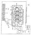
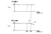
【解決手段】 ラインヘッド2には、有機EL素子からなる発光素子Eaを用いた発光素子ライン7が形成されている。制御回路3は、発光素子の駆動時間―発光光量の特性をメモリ6から読み出し、電流検出器5からフィードバックされた発光素子の検出電流と対比する。この際の検出電流は、各発光素子の発光光量に対応する。制御回路3は、前記メモリ6に記憶されている駆動時間―発光光量の特性と、検出電流に基づく現在の発光光量とを対比して特性をチェックし、発光光量が基準値よりも低下した場合には、印加電圧を昇圧して定電圧制御を行う。
【選択図】 図1
Description
Claims (13)
- 1ラインに配列される複数の有機EL素子からなる発光素子と、前記発光素子を定電圧制御する手段と、前記発光素子の駆動電流を共通して計測する駆動電流計測手段と、前記計測手段の計測値を用いて前記発光素子の特性をチェックする手段と、を具備することを特徴とするラインヘッド。
- 前記計測手段の計測値に基づいて、前記発光素子の発光光量をチェックすることを特徴とする、請求項1に記載のラインヘッド。
- 前記計測手段の計測値は、前記発光素子の電圧を制御する手段に入力されて、フィードバック制御で定電圧制御することを特徴とする、請求項1または請求項2に記載のラインヘッド。
- 前記計測手段の計測値に基づいて、前記発光素子の画素欠陥をチェックすることを特徴とする、請求項1に記載のラインヘッド。
- 前記計測手段の計測値に基づく特性チェックは、個別の発光素子毎に行うことを特徴とする、請求項1ないし請求項4のいずれかに記載のラインヘッド。
- 前記計測手段の計測値に基づく特性チェックは、1ラインに配列される複数の発光素子を複数のブロックに区分してブロック単位で行うことを特徴とする、請求項1ないし請求項4のいずれかに記載のラインヘッド。
- 前記計測手段の計測値に基づく特性チェックは、1ラインに配列される複数の発光素子に対して同時に行うことを特徴とする、請求項1ないし請求項4のいずれかに記載のラインヘッド。
- 前記各発光素子を駆動するFETのゲート電極とドレイン電極間に、コンデンサを接続したことを特徴とする、請求項1ないし請求項7のいずれかに記載のラインヘッド。
- 前記発光素子の定電圧制御は、前記発光素子の駆動時間が一定時間を超えて発光光量が低下した際に、発光光量を所定値に回復させるために段階的に昇圧して行われることを特徴とする、請求項1ないし請求項8のいずれかに記載のラインヘッド。
- 前記複数の発光素子が配列されるラインを副走査方向に複数列形成したことを特徴とする、請求項1ないし請求項9のいずれかに記載のラインヘッド。
- 像担持体の周囲に帯電手段と、請求項1ないし請求項10のいずれかに記載のラインヘッドと、現像手段と、転写手段との各画像形成用ユニットを配した画像形成ステーションを少なくとも2つ以上設け、転写媒体が各ステーションを通過することにより、タンデム方式で画像形成を行うことを特徴とする画像形成装置。
- 静電潜像を担持可能に構成された像担持体と、ロータリ現像ユニットと、請求項1ないし請求項10のいずれかに記載のラインヘッドとを備え、前記ロータリ現像ユニットは、複数のトナーカートリッジに収納されたトナーをその表面に担持するとともに、所定の回転方向に回転することによって異なる色のトナーを順次前記像担持体との対向位置に搬送し、前記像担持体と前記ロータリ現像ユニットとの間に現像バイアスを印加して、前記トナーを前記ロータリ現像ユニットから前記像担持体に移動させることで、前記静電潜像を顕像化してトナー像を形成することを特徴とする画像形成装置。
- 中間転写部材を備えたことを特徴とする、請求項11または請求項12に記載の画像形成装置。
Priority Applications (3)
| Application Number | Priority Date | Filing Date | Title |
|---|---|---|---|
| JP2004151306A JP2005329659A (ja) | 2004-05-21 | 2004-05-21 | ラインヘッドおよびそれを用いた画像形成装置 |
| EP05011031A EP1598200A3 (en) | 2004-05-21 | 2005-05-20 | Line head and image forming apparatus incorporating the same |
| US11/134,037 US20050263718A1 (en) | 2004-05-21 | 2005-05-20 | Line head and image forming apparatus incorporating the same |
Applications Claiming Priority (1)
| Application Number | Priority Date | Filing Date | Title |
|---|---|---|---|
| JP2004151306A JP2005329659A (ja) | 2004-05-21 | 2004-05-21 | ラインヘッドおよびそれを用いた画像形成装置 |
Publications (2)
| Publication Number | Publication Date |
|---|---|
| JP2005329659A true JP2005329659A (ja) | 2005-12-02 |
| JP2005329659A5 JP2005329659A5 (ja) | 2007-06-28 |
Family
ID=35484622
Family Applications (1)
| Application Number | Title | Priority Date | Filing Date |
|---|---|---|---|
| JP2004151306A Withdrawn JP2005329659A (ja) | 2004-05-21 | 2004-05-21 | ラインヘッドおよびそれを用いた画像形成装置 |
Country Status (1)
| Country | Link |
|---|---|
| JP (1) | JP2005329659A (ja) |
Cited By (5)
| Publication number | Priority date | Publication date | Assignee | Title |
|---|---|---|---|---|
| JP2007212545A (ja) * | 2006-02-07 | 2007-08-23 | Fujifilm Corp | 露光装置 |
| JP2008080643A (ja) * | 2006-09-27 | 2008-04-10 | Casio Comput Co Ltd | 露光装置及び画像形成装置並びに露光装置の動作方法 |
| US8446445B2 (en) | 2006-09-27 | 2013-05-21 | Casio Computer Co., Ltd. | Exposure device, image forming apparatus and method for operating exposure device |
| JP2015136919A (ja) * | 2014-01-24 | 2015-07-30 | コニカミノルタ株式会社 | 光書込み装置及び画像形成装置 |
| US20160001575A1 (en) * | 2014-07-07 | 2016-01-07 | Samsung Electronics Co., Ltd. | Image forming apparatus for determining defects of light-emitting element array chips |
Citations (6)
| Publication number | Priority date | Publication date | Assignee | Title |
|---|---|---|---|---|
| JPH03262658A (ja) * | 1990-03-14 | 1991-11-22 | Tokyo Electric Co Ltd | 電子写真装置 |
| JPH04128063A (ja) * | 1990-09-19 | 1992-04-28 | Hitachi Ltd | Ledアレイ発光装置 |
| JPH09199760A (ja) * | 1996-01-22 | 1997-07-31 | Canon Inc | 光量制御装置及び光量制御方法 |
| JPH11301020A (ja) * | 1998-04-21 | 1999-11-02 | Canon Inc | 発光装置および画像形成装置 |
| JP2003216110A (ja) * | 2001-11-13 | 2003-07-30 | Semiconductor Energy Lab Co Ltd | 表示装置 |
| JP2004114508A (ja) * | 2002-09-26 | 2004-04-15 | Seiko Epson Corp | 画像形成装置 |
-
2004
- 2004-05-21 JP JP2004151306A patent/JP2005329659A/ja not_active Withdrawn
Patent Citations (6)
| Publication number | Priority date | Publication date | Assignee | Title |
|---|---|---|---|---|
| JPH03262658A (ja) * | 1990-03-14 | 1991-11-22 | Tokyo Electric Co Ltd | 電子写真装置 |
| JPH04128063A (ja) * | 1990-09-19 | 1992-04-28 | Hitachi Ltd | Ledアレイ発光装置 |
| JPH09199760A (ja) * | 1996-01-22 | 1997-07-31 | Canon Inc | 光量制御装置及び光量制御方法 |
| JPH11301020A (ja) * | 1998-04-21 | 1999-11-02 | Canon Inc | 発光装置および画像形成装置 |
| JP2003216110A (ja) * | 2001-11-13 | 2003-07-30 | Semiconductor Energy Lab Co Ltd | 表示装置 |
| JP2004114508A (ja) * | 2002-09-26 | 2004-04-15 | Seiko Epson Corp | 画像形成装置 |
Cited By (9)
| Publication number | Priority date | Publication date | Assignee | Title |
|---|---|---|---|---|
| JP2007212545A (ja) * | 2006-02-07 | 2007-08-23 | Fujifilm Corp | 露光装置 |
| JP4660389B2 (ja) * | 2006-02-07 | 2011-03-30 | 富士フイルム株式会社 | 露光装置 |
| JP2008080643A (ja) * | 2006-09-27 | 2008-04-10 | Casio Comput Co Ltd | 露光装置及び画像形成装置並びに露光装置の動作方法 |
| US8446445B2 (en) | 2006-09-27 | 2013-05-21 | Casio Computer Co., Ltd. | Exposure device, image forming apparatus and method for operating exposure device |
| JP2015136919A (ja) * | 2014-01-24 | 2015-07-30 | コニカミノルタ株式会社 | 光書込み装置及び画像形成装置 |
| US20160001575A1 (en) * | 2014-07-07 | 2016-01-07 | Samsung Electronics Co., Ltd. | Image forming apparatus for determining defects of light-emitting element array chips |
| WO2016006813A1 (en) * | 2014-07-07 | 2016-01-14 | Samsung Electronics Co., Ltd. | Image forming apparatus for determining defects of light-emitting element array chips |
| US9844952B2 (en) | 2014-07-07 | 2017-12-19 | S-Printing Solution Co., Ltd. | Image forming apparatus for determining defects of light-emitting element array chips |
| EP2966507B1 (en) * | 2014-07-07 | 2019-07-03 | HP Printing Korea Co., Ltd. | Image forming apparatus for determining defects of light-emitting element array chips |
Similar Documents
| Publication | Publication Date | Title |
|---|---|---|
| US7911492B2 (en) | Line head and image forming apparatus incorporating the same | |
| JP2007190787A (ja) | ラインヘッドおよびそれを用いた画像形成装置 | |
| EP1598200A2 (en) | Line head and image forming apparatus incorporating the same | |
| KR100668274B1 (ko) | 화소 회로, 발광 장치 및 화상 형성 장치 | |
| JPH02501775A (ja) | トナー特性補償装置を備えたドットプリンタ | |
| JP2007030383A (ja) | 画像形成装置および画像形成方法 | |
| JP2005329659A (ja) | ラインヘッドおよびそれを用いた画像形成装置 | |
| JP2005329636A (ja) | ラインヘッドおよびそれを用いた画像形成装置 | |
| JP4434769B2 (ja) | ラインヘッドおよびそれを用いた画像形成装置 | |
| JP2005329634A (ja) | ラインヘッドおよびそれを用いた画像形成装置 | |
| JP2005329635A (ja) | ラインヘッドおよびそれを用いた画像形成装置 | |
| JP2005144685A (ja) | ラインヘッドおよびそれを用いた画像形成装置 | |
| JP2005144686A (ja) | ラインヘッドおよびそれを用いた画像形成装置 | |
| JP2007237572A (ja) | 画像形成装置および画像形成方法 | |
| JP2007210139A (ja) | ラインヘッドおよびそれを用いた画像形成装置 | |
| JP2005138351A (ja) | ラインヘッドおよびそれを用いた画像形成装置 | |
| JP2005096259A (ja) | ラインヘッドおよびそれを用いた画像形成装置 | |
| JP4561085B2 (ja) | ラインヘッドおよびそれを用いた画像形成装置 | |
| JP2005329660A (ja) | ラインヘッドおよびそれを用いた画像形成装置 | |
| JP4296402B2 (ja) | ラインヘッドおよびそれを用いた画像形成装置 | |
| JP4888671B2 (ja) | ラインヘッドおよびそれを用いた画像形成装置 | |
| JP2007230004A (ja) | 電気光学装置及び電子機器 | |
| JP4434770B2 (ja) | ラインヘッドおよびそれを用いた画像形成装置 | |
| JP2005062325A (ja) | 画像形成装置および画像形成方法 | |
| JP2007276332A (ja) | ラインヘッド及びその駆動方法並びに画像形成装置 |
Legal Events
| Date | Code | Title | Description |
|---|---|---|---|
| A521 | Request for written amendment filed |
Free format text: JAPANESE INTERMEDIATE CODE: A523 Effective date: 20070514 |
|
| A621 | Written request for application examination |
Free format text: JAPANESE INTERMEDIATE CODE: A621 Effective date: 20070514 |
|
| A977 | Report on retrieval |
Free format text: JAPANESE INTERMEDIATE CODE: A971007 Effective date: 20090727 |
|
| A131 | Notification of reasons for refusal |
Free format text: JAPANESE INTERMEDIATE CODE: A131 Effective date: 20090729 |
|
| A761 | Written withdrawal of application |
Free format text: JAPANESE INTERMEDIATE CODE: A761 Effective date: 20090904 |