JP2005294881A - 同軸・導波管変換構造及びその製造方法 - Google Patents
同軸・導波管変換構造及びその製造方法 Download PDFInfo
- Publication number
- JP2005294881A JP2005294881A JP2004102410A JP2004102410A JP2005294881A JP 2005294881 A JP2005294881 A JP 2005294881A JP 2004102410 A JP2004102410 A JP 2004102410A JP 2004102410 A JP2004102410 A JP 2004102410A JP 2005294881 A JP2005294881 A JP 2005294881A
- Authority
- JP
- Japan
- Prior art keywords
- coaxial
- conductor
- hole
- waveguide
- mode transmission
- Prior art date
- Legal status (The legal status is an assumption and is not a legal conclusion. Google has not performed a legal analysis and makes no representation as to the accuracy of the status listed.)
- Granted
Links
- 238000006243 chemical reaction Methods 0.000 title claims abstract description 36
- 238000004519 manufacturing process Methods 0.000 title claims abstract description 20
- 239000004020 conductor Substances 0.000 claims abstract description 97
- 230000005540 biological transmission Effects 0.000 claims abstract description 94
- 238000010030 laminating Methods 0.000 claims abstract description 15
- 230000002093 peripheral effect Effects 0.000 claims description 6
- 239000003989 dielectric material Substances 0.000 claims description 3
- 238000000034 method Methods 0.000 description 14
- 238000010168 coupling process Methods 0.000 description 7
- 230000008569 process Effects 0.000 description 6
- 230000008878 coupling Effects 0.000 description 5
- 238000005859 coupling reaction Methods 0.000 description 5
- 230000015572 biosynthetic process Effects 0.000 description 2
- 238000005553 drilling Methods 0.000 description 2
- -1 polytetrafluoroethylene Polymers 0.000 description 2
- 229920001343 polytetrafluoroethylene Polymers 0.000 description 2
- 239000004810 polytetrafluoroethylene Substances 0.000 description 2
- 229910000881 Cu alloy Inorganic materials 0.000 description 1
- 230000008901 benefit Effects 0.000 description 1
- 238000005219 brazing Methods 0.000 description 1
- 230000008859 change Effects 0.000 description 1
- 239000000463 material Substances 0.000 description 1
- 238000012986 modification Methods 0.000 description 1
- 230000004048 modification Effects 0.000 description 1
- 238000007747 plating Methods 0.000 description 1
- 239000011347 resin Substances 0.000 description 1
- 229920005989 resin Polymers 0.000 description 1
- 239000000758 substrate Substances 0.000 description 1
Images

Landscapes
- Waveguides (AREA)
Abstract
【解決手段】 少なくとも1つに貫通孔12を有する複数の誘電体部材を積層して少なくとも第1の面側に貫通孔12が露出する積層体11を形成する第1のステップと、貫通孔12の周囲を除く前記積層体11の前記第1の面及び前記第1の面に対向する第2の面、並びに前記貫通孔12に導体を設ける第2のステップと、を含むことにより、前記貫通孔内の導体13bに中心導体23が接続される同軸モード伝送路20と前記第1の面及び前記第2の面に設けられた導体13を周囲導体として備える導波管モード伝送路との変換構造を形成することを特徴とする同軸・導波管変換構造の製造方法を用いる。
【選択図】 図5
Description
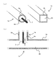
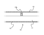
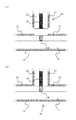
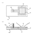
11、11a、11b、11c、11d、11e 誘電体
12 貫通孔
13 周囲導体
20、44 同軸モード伝送路
21 周囲導体
23、45 中心導体
40 同軸・導波管変換構造
41 平面アンテナ
42 壁部材
43 導波路
L 中心導体が突出する所定深さ
t1 第1の誘電体の厚さ
t2 第2の誘電体の厚さ
Claims (7)
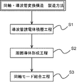
- 少なくとも1つに貫通孔を有する複数の誘電体部材を積層して少なくとも第1の面側に前記貫通孔が露出する積層体を形成する第1のステップと、
前記貫通孔の周囲を除く前記積層体の前記第1の面及び前記第1の面に対向する第2の面、並びに前記貫通孔に導体を設ける第2のステップと、
を含むことにより、前記貫通孔内の導体に中心導体が接続される同軸モード伝送路と前記第1の面及び前記第2の面に設けられた導体を周囲導体として備える導波管モード伝送路との変換構造を形成することを特徴とする同軸・導波管変換構造の製造方法。 - 前記第1のステップは、貫通孔を有する第1の誘電体部材と貫通孔を持たない第2の誘電体部材とを積層するステップを含むことを特徴とする請求項1記載の同軸・導波管変換構造の製造方法。
- 前記第1のステップは、貫通孔を有する複数の誘電体部材を、これらの貫通孔が一列に配置されかつ全体として所定の深さを有するように積層するステップを含むことを特徴とする請求項1記載の同軸・導波管変換構造の製造方法。
- 少なくとも1つに貫通孔を有する複数の誘電体部材が、前記貫通孔が表面に露出するように積層された積層体と、
前記貫通孔の周囲を除く前記積層体の第1の面及び前記第1の面と対向する第2の面に設けられ、導波管モード伝送路の周囲導体の一部をなす第1の導体と、
前記貫通孔内に設けられかつ同軸モード伝送路の中心導体と接続される第2の導体と、
を有する同軸・導波管変換構造。 - 中心導体が前記貫通孔内の前記第2の導体と接続されるとともに、周囲導体が前記第1の面に設けられた前記第1の導体と接続される同軸モード伝送路を更に有することを特徴とする請求項4記載の同軸・導波管変換構造。
- 前記積層体は、所定の深さの貫通孔を有する第1の誘電体部材と貫通孔を持たない第2の誘電体部材とを含むことを特徴とする請求項4または5に記載の同軸・導波管変換構造。
- 前記積層体は、貫通孔を有する複数の誘電体部材を含み、これらの貫通孔は一列に配置されかつ全体として所定の深さを有していることを特徴とする請求項4または5に記載の同軸・導波管変換構造。
Priority Applications (1)
| Application Number | Priority Date | Filing Date | Title |
|---|---|---|---|
| JP2004102410A JP4133906B2 (ja) | 2004-03-31 | 2004-03-31 | 同軸・導波管変換構造の製造方法 |
Applications Claiming Priority (1)
| Application Number | Priority Date | Filing Date | Title |
|---|---|---|---|
| JP2004102410A JP4133906B2 (ja) | 2004-03-31 | 2004-03-31 | 同軸・導波管変換構造の製造方法 |
Publications (2)
| Publication Number | Publication Date |
|---|---|
| JP2005294881A true JP2005294881A (ja) | 2005-10-20 |
| JP4133906B2 JP4133906B2 (ja) | 2008-08-13 |
Family
ID=35327387
Family Applications (1)
| Application Number | Title | Priority Date | Filing Date |
|---|---|---|---|
| JP2004102410A Expired - Lifetime JP4133906B2 (ja) | 2004-03-31 | 2004-03-31 | 同軸・導波管変換構造の製造方法 |
Country Status (1)
| Country | Link |
|---|---|
| JP (1) | JP4133906B2 (ja) |
Cited By (3)
| Publication number | Priority date | Publication date | Assignee | Title |
|---|---|---|---|---|
| JP2012175624A (ja) * | 2011-02-24 | 2012-09-10 | Amushisu:Kk | ポスト壁導波路アンテナ及びアンテナモジュール |
| WO2014126194A1 (ja) * | 2013-02-18 | 2014-08-21 | 株式会社フジクラ | モード変換器及びその製造方法 |
| CN110165350A (zh) * | 2019-06-06 | 2019-08-23 | 西南应用磁学研究所 | 小型化波导同轴转换装置 |
-
2004
- 2004-03-31 JP JP2004102410A patent/JP4133906B2/ja not_active Expired - Lifetime
Cited By (6)
| Publication number | Priority date | Publication date | Assignee | Title |
|---|---|---|---|---|
| JP2012175624A (ja) * | 2011-02-24 | 2012-09-10 | Amushisu:Kk | ポスト壁導波路アンテナ及びアンテナモジュール |
| WO2014126194A1 (ja) * | 2013-02-18 | 2014-08-21 | 株式会社フジクラ | モード変換器及びその製造方法 |
| JP2014158243A (ja) * | 2013-02-18 | 2014-08-28 | Fujikura Ltd | モード変換器の製造方法 |
| US10511077B2 (en) | 2013-02-18 | 2019-12-17 | Fujikura Ltd. | Method for manufacturing mode converter |
| CN110165350A (zh) * | 2019-06-06 | 2019-08-23 | 西南应用磁学研究所 | 小型化波导同轴转换装置 |
| CN110165350B (zh) * | 2019-06-06 | 2024-01-16 | 西南应用磁学研究所 | 小型化波导同轴转换装置 |
Also Published As
| Publication number | Publication date |
|---|---|
| JP4133906B2 (ja) | 2008-08-13 |
Similar Documents
| Publication | Publication Date | Title |
|---|---|---|
| KR101756124B1 (ko) | 크로스 커플링 노치 구조를 구비한 캐비티 타입의 무선 주파수 필터 | |
| JP6105496B2 (ja) | 一括積層基板 | |
| JP5947917B2 (ja) | モード変換器 | |
| CN111433971A (zh) | 高频传输线路 | |
| JP2018186204A (ja) | 高周波モジュール、無線装置、及び高周波モジュールの製造方法 | |
| JP2012029163A (ja) | アレーアンテナ及びその製造方法 | |
| JP6353762B2 (ja) | 回路基板 | |
| JP6190932B1 (ja) | 伝送線路 | |
| JP2008193243A (ja) | 導波管 | |
| JP4133906B2 (ja) | 同軸・導波管変換構造の製造方法 | |
| JP2008262989A (ja) | 高周波回路基板 | |
| JP2008193162A (ja) | マイクロストリップ線路−導波管変換器 | |
| EP3707974B1 (en) | Spiral antenna and related fabrication techniques | |
| US20170125890A1 (en) | Three-dimensional antenna apparatus | |
| KR101892456B1 (ko) | 차량용 레이더 안테나 피시비 제조 방법 | |
| JP4904336B2 (ja) | レーダ装置用アンテナおよびその製造方法 | |
| JP2008193161A (ja) | マイクロストリップ線路−導波管変換器 | |
| US20200067195A1 (en) | Antenna system | |
| JP2021072413A (ja) | アンテナモジュール | |
| CN212874751U (zh) | 一种具有阻抗匹配功能的天线辐射单元 | |
| JP5753294B1 (ja) | コルゲートホーン | |
| JP2011040804A (ja) | 誘電体導波管の接続構造 | |
| JP4990021B2 (ja) | 高周波伝送線路 | |
| JP2015188143A (ja) | 導波管およびその製造方法 | |
| CN100574006C (zh) | 螺旋式天线及螺旋式天线的制造方法 |
Legal Events
| Date | Code | Title | Description |
|---|---|---|---|
| A621 | Written request for application examination |
Free format text: JAPANESE INTERMEDIATE CODE: A621 Effective date: 20060913 |
|
| A977 | Report on retrieval |
Free format text: JAPANESE INTERMEDIATE CODE: A971007 Effective date: 20070927 |
|
| A131 | Notification of reasons for refusal |
Free format text: JAPANESE INTERMEDIATE CODE: A131 Effective date: 20071218 |
|
| A521 | Request for written amendment filed |
Free format text: JAPANESE INTERMEDIATE CODE: A523 Effective date: 20080129 |
|
| A02 | Decision of refusal |
Free format text: JAPANESE INTERMEDIATE CODE: A02 Effective date: 20080226 |
|
| A521 | Request for written amendment filed |
Free format text: JAPANESE INTERMEDIATE CODE: A523 Effective date: 20080312 |
|
| A911 | Transfer to examiner for re-examination before appeal (zenchi) |
Free format text: JAPANESE INTERMEDIATE CODE: A911 Effective date: 20080423 |
|
| TRDD | Decision of grant or rejection written | ||
| A01 | Written decision to grant a patent or to grant a registration (utility model) |
Free format text: JAPANESE INTERMEDIATE CODE: A01 Effective date: 20080520 |
|
| A01 | Written decision to grant a patent or to grant a registration (utility model) |
Free format text: JAPANESE INTERMEDIATE CODE: A01 |
|
| A61 | First payment of annual fees (during grant procedure) |
Free format text: JAPANESE INTERMEDIATE CODE: A61 Effective date: 20080602 |
|
| FPAY | Renewal fee payment (event date is renewal date of database) |
Free format text: PAYMENT UNTIL: 20110606 Year of fee payment: 3 |
|
| R150 | Certificate of patent or registration of utility model |
Free format text: JAPANESE INTERMEDIATE CODE: R150 Ref document number: 4133906 Country of ref document: JP Free format text: JAPANESE INTERMEDIATE CODE: R150 |
|
| FPAY | Renewal fee payment (event date is renewal date of database) |
Free format text: PAYMENT UNTIL: 20110606 Year of fee payment: 3 |
|
| FPAY | Renewal fee payment (event date is renewal date of database) |
Free format text: PAYMENT UNTIL: 20120606 Year of fee payment: 4 |
|
| FPAY | Renewal fee payment (event date is renewal date of database) |
Free format text: PAYMENT UNTIL: 20120606 Year of fee payment: 4 |
|
| FPAY | Renewal fee payment (event date is renewal date of database) |
Free format text: PAYMENT UNTIL: 20130606 Year of fee payment: 5 |
|
| FPAY | Renewal fee payment (event date is renewal date of database) |
Free format text: PAYMENT UNTIL: 20130606 Year of fee payment: 5 |
|
| FPAY | Renewal fee payment (event date is renewal date of database) |
Free format text: PAYMENT UNTIL: 20140606 Year of fee payment: 6 |
|
| R250 | Receipt of annual fees |
Free format text: JAPANESE INTERMEDIATE CODE: R250 |
|
| R250 | Receipt of annual fees |
Free format text: JAPANESE INTERMEDIATE CODE: R250 |
|
| R250 | Receipt of annual fees |
Free format text: JAPANESE INTERMEDIATE CODE: R250 |
|
| EXPY | Cancellation because of completion of term |