JP2005294796A - Light emitting element storage package, light emitting device, and lighting device - Google Patents
Light emitting element storage package, light emitting device, and lighting device Download PDFInfo
- Publication number
- JP2005294796A JP2005294796A JP2004275058A JP2004275058A JP2005294796A JP 2005294796 A JP2005294796 A JP 2005294796A JP 2004275058 A JP2004275058 A JP 2004275058A JP 2004275058 A JP2004275058 A JP 2004275058A JP 2005294796 A JP2005294796 A JP 2005294796A
- Authority
- JP
- Japan
- Prior art keywords
- light
- light emitting
- emitting element
- emitting device
- phosphor
- Prior art date
- Legal status (The legal status is an assumption and is not a legal conclusion. Google has not performed a legal analysis and makes no representation as to the accuracy of the status listed.)
- Pending
Links
Images
Landscapes
- Arrangement Of Elements, Cooling, Sealing, Or The Like Of Lighting Devices (AREA)
- Non-Portable Lighting Devices Or Systems Thereof (AREA)
- Led Device Packages (AREA)
Abstract
【課題】 蛍光体による波長変換効率を向上させ 発光装置の光出力を高めるとともに発光素子から発光される光を外部に効率良く放射できるようにし、輝度や演色性等の照明特性に優れた発光装置を提供することである。
【解決手段】 上面に発光素子4の載置部2aが形成されたセラミックスから成る基体2と、この基体2の上面の外周部に載置部2aを囲繞するように接合されるとともに内周面が反射面とされている枠体3と、一端が基体2の上面に形成されて発光素子4の電極に電気的に接続されるとともに他端が基体2の側面または下面に導出される配線導体と、枠体3の貫通孔に発光素子4を覆うように設けられ、発光素子4が発光する光を波長変換する蛍光体を含有する透光性部材5とを具備しており、基体2のセラミックスに含まれる結晶粒の平均粒径が1乃至5μmである。
【選択図】 図1
PROBLEM TO BE SOLVED: To improve the wavelength conversion efficiency by a phosphor and increase the light output of the light emitting device and efficiently radiate light emitted from the light emitting element to the outside, and is excellent in illumination characteristics such as luminance and color rendering properties. Is to provide.
SOLUTION: A base body 2 made of ceramics having a mounting portion 2a of a light emitting element 4 formed on an upper surface, and an outer peripheral portion of the upper surface of the base body 2 joined to surround the mounting portion 2a and an inner peripheral surface. And a wiring conductor in which one end is formed on the upper surface of the base 2 and is electrically connected to the electrode of the light emitting element 4 and the other end is led to the side surface or the lower surface of the base 2. And a translucent member 5 that includes a phosphor that is provided in a through hole of the frame 3 so as to cover the light emitting element 4 and that converts the wavelength of light emitted from the light emitting element 4. The average grain size of the crystal grains contained in the ceramic is 1 to 5 μm.
[Selection] Figure 1
Description
本発明は、発光素子から発光される光を蛍光体で波長変換し外部に放射する発光素子収納用パッケージおよび発光装置ならびに照明装置に関する。 The present invention relates to a light-emitting element storage package, a light-emitting device, and an illumination device that convert the wavelength of light emitted from a light-emitting element with a phosphor and emit the light to the outside.
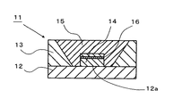
従来の発光ダイオード(LED)等の発光素子14から発光される近紫外光や青色光等の光を赤色,緑色,青色および黄色等の複数の蛍光体(図示せず)で波長変換して白色発光する発光装置11を図2に示す。図2において、発光装置11は、上面の中央部に発光素子14を載置するための載置部12aを有し、載置部12aおよびその周辺から発光装置の内外を電気的に導通接続するリード端子やメタライズ配線等からなる配線導体(図示せず)が形成された絶縁体から成る基体12と、基体12の上面に接着固定され、上側開口が下側開口より大きい貫通孔が形成されているとともに、内周面が発光素子14から発光される光を反射する反射面とされている枠状の枠体13と、枠体13の内側に充填され発光素子14から発光される光によって励起され波長変換する蛍光体を含有した透光性部材15と、載置部12aに載置固定された発光素子14とから主に構成されている。
Light is converted into white by converting wavelengths of light such as near-ultraviolet light and blue light emitted from a
基体12は、酸化アルミニウム質焼結体(アルミナセラミックス),窒化アルミニウム質焼結体,ムライト質焼結体またはガラスセラミックス等のセラミックス、あるいはエポキシ樹脂等の樹脂から成る。基体12がセラミックスから成る場合、その上面に配線導体がタングステン(W)やモリブデン(Mo)−マンガン(Mn)等から成る金属ペーストを高温で焼成して形成される。また、基体12が樹脂から成る場合、銅(Cu)や鉄(Fe)−ニッケル(Ni)合金等から成るリード端子がモールド成型されて基体12の内部に設置固定される。
The
また、枠体13は、上側開口が下側開口より大きい貫通孔が形成されるとともに内周面に光を反射する反射面が設けられる枠状となっている。具体的には、アルミニウム(Al)やFe−Ni−コバルト(Co)合金等の金属、アルミナセラミックス等のセラミックスまたはエポキシ樹脂等の樹脂から成り、切削加工、金型成型または押し出し成型等の成形技術により形成される。
Further, the
さらに、枠体13の反射面は、貫通孔の内周面を研磨して平坦化することにより、あるいは、貫通孔の内周面にAl等の金属を蒸着法やメッキ法により被着することにより形成される。そして、枠体13は、半田や銀(Ag)ろう等のろう材もしくは樹脂接着材等の接合材により、載置部12aを枠体13の内周面で取り囲むように基体12の上面に接合される。
Further, the reflecting surface of the
そして、載置部12aの周辺に配置した配線導体と発光素子14とをボンディングワイヤや金属ボール等の電気接続手段(図示せず)を介して電気的に接続し、しかる後、蛍光体を含有するエポキシ樹脂やシリコーン樹脂等の透光性部材15をディスペンサー等の注入機で発光素子14を覆うように枠体13の内側に充填しオーブンで熱硬化させることで、発光素子14から発光された光を蛍光体により波長変換し所望の波長スペクトルを有する光を取り出せる発光装置11とすることができる。
図2に示す従来の発光装置11では、発光素子14から発光される光を効率よく発光装置11の外部に放射させるために、例えば、セラミックスから成る基体12の上面を研磨加工で平滑にしたり、基体12の上面にAg,AlまたはAu等の金属膜を形成したりして基体12の上面の反射率を向上させていた。しかし、透光性部材15の内部に蛍光体を含有させて発光素子14から発光される光を波長変換させる発光装置11の場合、発光素子14から発光される光が透光性部材15を透過して基体12の上面で正反射することにより、正反射方向以外の蛍光体は励起され難く、一部の蛍光体で主に波長変換するために波長変換の効率が低くなって光出力や輝度、演色性が低下するという問題点を有していた。
In the conventional
また、基体12がセラミックスから成る場合、基板12に光が吸収されることにより、基体12の上面における反射率が低下し易くなる。その結果、発光装置は所望の光出力が得られなくなるとともに、近年に望まれている光取り出し効率を達し得ないという問題点も有していた。また基板12による光吸収を防止するため基体12の上面に金属膜を形成する場合、めっきや蒸着等により金属膜を形成する必要があり、製造工程が多くなるとともに製造コストが高くなるという問題も有していた。
Further, when the
また、基体12がエポキシ樹脂や液晶ポリマー等の樹脂材料から成る場合、発光素子14が発する熱を基体12を介して効率良く外部に放散できないことから、その熱により発光素子14の発光効率が著しく低下し、その結果、発光装置11の光出力が低下するという問題点を有していた。
In addition, when the
さらに、発光素子14を被覆するとともに発光素子14から発光される光を波長変換するための蛍光体を含有した透光性部材15において、蛍光体の含有率を上げて波長変換の効率を向上させようとすると、発光装置から放射される光が蛍光体によって妨害され易くなるため、光出力を高めることができないという問題点を有していた。また逆に、蛍光体の含有率を下げると、波長変換の効率が低下して所望の波長の光が得られず、その結果、光出力を高めることができないという問題点を有していた。
Furthermore, in the
したがって、本発明は上記問題点に鑑みて完成されたものであり、その目的は、蛍光体による波長変換効率を向上させて発光装置の光出力を高めるとともに発光素子から発光される光を外部に効率良く放射できるようにし、輝度や演色性等の照明特性に優れた発光装置を提供することである。 Accordingly, the present invention has been completed in view of the above problems, and its purpose is to improve the wavelength conversion efficiency by the phosphor to increase the light output of the light emitting device and to transmit the light emitted from the light emitting element to the outside. An object is to provide a light-emitting device that can radiate efficiently and has excellent illumination characteristics such as luminance and color rendering.
本発明の発光素子収納用パッケージは、上面に発光素子の載置部が形成されたセラミックスから成る基体と、該基体の上面の外周部に前記載置部を囲繞するように接合されるとともに内周面が前記発光素子から発光される光を反射する反射面とされている枠体と、一端が前記上面に形成されて前記発光素子の電極に電気的に接続されるとともに他端が前記基体の側面または下面に導出される配線導体と、前記枠体の内側に前記発光素子を覆うように設けられ、前記発光素子が発光する光を波長変換する蛍光体を含有する透光性部材とを具備しており、前記基体は、前記セラミックスに含まれる結晶粒の平均粒径が1乃至5μmであることを特徴とする。 The light emitting element storage package according to the present invention includes a base body made of ceramics having a light emitting element mounting portion formed on an upper surface, and an outer peripheral portion of the upper surface of the base body that is joined so as to surround the mounting portion. A frame having a peripheral surface as a reflection surface for reflecting light emitted from the light emitting element, one end formed on the upper surface and electrically connected to an electrode of the light emitting element, and the other end at the base And a translucent member containing a phosphor that is provided inside the frame so as to cover the light emitting element and converts the wavelength of light emitted from the light emitting element. The substrate is characterized in that the average grain size of crystal grains contained in the ceramic is 1 to 5 μm.
本発明の発光素子収納用パッケージにおいて、好ましくは、前記透光性部材の上面と前記発光素子の発光部との間の距離が0.1乃至0.8mmであることを特徴とする。 In the light emitting element storage package of the present invention, it is preferable that a distance between an upper surface of the light transmissive member and a light emitting portion of the light emitting element is 0.1 to 0.8 mm.
本発明の発光装置は、上記本発明の発光素子収納用パッケージと、前記載置部に載置されるとともに前記配線導体に電気的に接続された発光素子とを具備していることを特徴とする。 A light emitting device of the present invention comprises the light emitting element storage package of the present invention, and a light emitting element mounted on the mounting portion and electrically connected to the wiring conductor. To do.
本発明の照明装置は、上記本発明の発光装置を所定の配置となるように設置したことを特徴とする。 The illuminating device of the present invention is characterized in that the light emitting device of the present invention is installed in a predetermined arrangement.
本発明の発光素子収納用パッケージによれば、基体はセラミックスに含まれる結晶粒の平均粒径が1乃至5μmであることから、結晶粒が非常に高密度になるため結晶粒間の粒界や気孔が非常に小さいものとなり、基体の表面の結晶粒が占める割合が大きくなるので、発光素子から発光された光が基体の内部に入り込むのを有効に抑制して反射率を高めることができ、その結果、発光装置の光出力を高めることができる。 According to the light emitting element storage package of the present invention, since the average grain size of the crystal grains contained in the ceramic is 1 to 5 μm, the crystal grains have a very high density. Since the pores are very small and the proportion of crystal grains on the surface of the substrate is large, it is possible to effectively suppress the light emitted from the light emitting element from entering the inside of the substrate and increase the reflectance, As a result, the light output of the light emitting device can be increased.
また、基体の表面を高密度に占める結晶粒によって基体の表面に適度に凹凸が形成されるため、発光素子から発光される光を適度に乱反射させてより多くの蛍光体に光を照射させることができる。その結果、波長変換効率を向上させることができ、光出力や輝度、演色性を高めることができる。 In addition, since the surface of the substrate is moderately uneven due to the crystal grains occupying the surface of the substrate at a high density, the light emitted from the light emitting element is appropriately diffusely reflected to irradiate more phosphors. Can do. As a result, the wavelength conversion efficiency can be improved, and the light output, luminance, and color rendering can be improved.
さらに、高密度の結晶粒によって基体が構成されているため、基体の熱伝導率が向上し、発光素子の発する熱が基体を介して効率良く外部に放散することができるので、熱に起因する発光素子の発光効率の低下を有効に抑制できる。よって、発光装置の光出力が低下することを抑制できる。 Furthermore, since the base is composed of high-density crystal grains, the thermal conductivity of the base is improved, and the heat generated by the light-emitting element can be efficiently dissipated outside through the base, resulting in heat. A decrease in light emission efficiency of the light emitting element can be effectively suppressed. Therefore, it can suppress that the light output of a light-emitting device falls.
本発明の発光素子収納用パッケージによれば、好ましくは、透光性部材の上面と発光素子の発光部との間の距離が0.1乃至0.8mmであることから、発光素子から発光された光を透光性部材に含まれる蛍光体によって高効率に波長変換することができるとともに、それらの波長変換された光を蛍光体に妨害されるのを有効に抑制して透光性部材の外部に高効率に放射することができる輝度や演色性等の照明特性を非常に良好なものとすることができる。 According to the light emitting element storage package of the present invention, it is preferable that the distance between the upper surface of the translucent member and the light emitting portion of the light emitting element is 0.1 to 0.8 mm. The wavelength of the transmitted light can be converted with high efficiency by the phosphor contained in the translucent member, and the wavelength-converted light is effectively prevented from being obstructed by the phosphor. Illumination characteristics such as brightness and color rendering that can be radiated to the outside with high efficiency can be made very good.
本発明の発光装置によれば、本発明の発光素子収納用パッケージと、載置部に載置されるとともに配線導体に電気的に接続された発光素子とを具備していることから、発光素子から発光される光を効率よく反射し、蛍光体を多く励起させることができ、光出力が高く、輝度や演色性等の照明特性が非常に優れたものとすることができる。 According to the light emitting device of the present invention, the light emitting device includes the light emitting element storage package of the present invention and the light emitting element mounted on the mounting portion and electrically connected to the wiring conductor. Can efficiently reflect the light emitted from the light source, excite many phosphors, have high light output, and have excellent illumination characteristics such as luminance and color rendering.
本発明の照明装置は、上記本発明の発光装置を所定の配置となるように設置したことから、半導体から成る発光素子の電子の再結合による発光を利用しているため、従来の放電を用いた照明装置よりも低消費電力かつ長寿命とすることが可能な小型の照明装置とすることができる。その結果、発光素子から発生する光の中心波長の変動を抑制することができ、長期間にわたり安定した放射光強度かつ放射光角度(配光分布)で光を照射することができるとともに、照射面における色むらや照度分布の偏りが抑制された照明装置とすることができる。 Since the light emitting device of the present invention is installed in a predetermined arrangement, the lighting device of the present invention uses light emission by recombination of electrons of a light emitting element made of a semiconductor. Thus, a small illuminating device that can have lower power consumption and longer life than the existing illuminating device can be obtained. As a result, fluctuations in the center wavelength of light generated from the light emitting element can be suppressed, light can be emitted with a stable radiant light intensity and radiant light angle (light distribution distribution) over a long period of time, and an irradiation surface It is possible to provide a lighting device in which uneven color and uneven illuminance distribution are suppressed.
また、本発明の発光装置を光源として所定の配置に設置するとともに、これらの発光装置の周囲に任意の形状に光学設計した反射治具や光学レンズ、光拡散板等を設置することにより、任意の配光分布の光を放射する照明装置とすることができる。 In addition, the light emitting device of the present invention is installed in a predetermined arrangement as a light source, and by installing a reflection jig, an optical lens, a light diffusing plate, etc. optically designed in an arbitrary shape around these light emitting devices, It can be set as the illuminating device which radiates | emits the light of this light distribution.
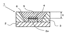
本発明の発光素子収納用パッケージ(以下、パッケージともいう)および発光装置について以下に詳細に説明する。図1は本発明の発光装置1の実施の形態の一例を示す断面図である。この図において、2は基体、3は枠体、4は発光素子、5は蛍光体(図示せず)を含有した透光性部材であり、主としてこれらで発光素子4から発光される光を外部に出力させ得る発光装置1が構成される。
A light emitting element storage package (hereinafter also referred to as a package) and a light emitting device of the present invention will be described in detail below. FIG. 1 is a sectional view showing an example of an embodiment of a
本発明のパッケージは、上面に発光素子4の載置部2aが形成されたセラミックスから成る基体2と、この基体2の上面の外周部に載置部2aを囲繞するように接合されるとともに内周面が発光素子4から発光される光を反射する反射面とされている枠体3と、一端が基体2の上面に形成されて発光素子4の電極に電気的に接続されるとともに他端が基体2の側面または下面に導出される配線導体(図示せず)と、枠体3の内側に発光素子4を覆うように設けられるとともに、発光素子4から発光される光を波長変換する蛍光体を含有する透光性部材5とを具備している。
The package of the present invention is bonded to the
基体2は、酸化アルミニウム質焼結体,窒化アルミニウム質焼結体,ムライト質焼結体またはガラスセラミックス等のセラミックスから成る絶縁体から成り、発光素子4を支持する支持部材として機能し、その上面に発光素子4を搭載するための搭載部2aを有している。
The
また、基体2は、セラミックスの結晶粒の平均粒径が1乃至5μmである。これにより、結晶粒が非常に高密度になるため基体2の表面の結晶粒が占める割合が大きくなり、結晶粒間から基体2の内部に入り込む光が有効に抑制されて基体2の上面の反射率が向上するので、発光装置1の光出力を高めることができる。
The
さらに、基体2の上面の算術平均粗さが、発光素子4から発光された光を基体2の上面で全方向に反射することができる適度な大きさとなる。その結果、枠体3の内周面で反射される光により励起されて発光する蛍光体の数が増加し、発光装置1の光出力や輝度、演色性を高めることができる。
Furthermore, the arithmetic average roughness of the upper surface of the
なお、セラミックスの結晶粒の平均粒径が5μmより大きい場合、基体2の表面の結晶粒が占める割合が小さくなり、結晶粒間から基体2内部に入り込む光が増加して基体2の上面における反射率が低下し易くなる。その結果、発光素子4から発光された光や蛍光体から発光された光が基体2の上面で効率よく反射されずに発光装置1の光出力が低下し易くなる。また、セラミックスの結晶粒の平均粒径が1μmより小さい場合、基体2の上面の算術平均粗さが小さくなり、発光素子4から発光される光が基体2の上面で正反射し易くなって、全方向へ反射することが困難となる。その結果、正反射方向以外の蛍光体が励起され難くなって、正反射方向に位置する蛍光体が主に波長変換に寄与することとなり波長変換の効率が低くなって、発光装置1の光出力が低下し易くなる。
When the average grain size of the ceramic crystal grains is larger than 5 μm, the proportion of the crystal grains on the surface of the
また、基体2は、セラミックスの結晶粒の平均粒径が1乃至5μmであることから、基体2の熱伝導性の高い結晶粒の密度が高くなって、基体2の熱伝導率が向上するため発光素子4の発する熱を基体2を介して効率良く外部に放散することが可能となる。そのため、熱に起因する発光素子4の発光効率の低下を抑制できることから、発光装置1の光出力の低下を有効に抑制できる。
In addition, since the
載置部2aには、発光素子4が電気的に接続されるための配線導体(図示せず)が形成されている。この配線導体が基体2の内部に形成された配線層(図示せず)を介して発光装置1の外表面に導出され、ろう材や金属製のリード等を介して外部電気回路基板に接続されることにより、発光素子4と外部電気回路とが電気的に接続される。
A wiring conductor (not shown) for electrically connecting the light emitting element 4 is formed on the mounting
発光素子4を配線導体に接続する手段としては、Au線やAl線等によるワイヤを介して接続するワイヤボンディング方式、あるいは発光素子4の下面に形成した電極を、Au−錫(Sn)半田,Sn−Ag半田,Sn−Ag−Cu半田またはSn−鉛(Pb)等を用いた半田バンプ、またはAuやAg等の金属を用いた金属バンプから成る接続手段を介して接続するフリップチップボンディング方式等の方法が用いられる。好ましくは、フリップチップボンディング方式により接続するのがよい。これにより、配線導体を基体2の上面の発光素子4の直下に設けることができるため、基体2の上面の発光素子4の周辺部に配線導体の領域を設ける必要がなくなる。よって、発光素子4から発光された光がこの基体2の配線導体の領域で吸収されて放射される光出力が低下するのを有効に抑制することができる。
As a means for connecting the light emitting element 4 to the wiring conductor, a wire bonding method of connecting via a wire such as an Au wire or an Al wire, or an electrode formed on the lower surface of the light emitting element 4 is made of Au-tin (Sn) solder, Flip chip bonding method in which connection is made through a connection means comprising solder bumps using Sn-Ag solder, Sn-Ag-Cu solder, Sn-lead (Pb), or metal bumps using a metal such as Au or Ag. Etc. are used. Preferably, the connection is made by a flip chip bonding method. Accordingly, since the wiring conductor can be provided immediately below the light emitting element 4 on the upper surface of the
配線導体は、W,Mo,Mn,CuまたはAg等の金属粉末から成るメタライズ層から成り、基体2の表面や内部に形成される。または、Fe−Ni−Co合金等のリード端子を基体2に埋設することにより形成されてもよい。さらに、配線導体が形成された絶縁体から成る入出力端子を基体2に設けられた貫通孔に嵌着接合させることによって設けられてもよい。
The wiring conductor is made of a metallized layer made of a metal powder such as W, Mo, Mn, Cu, or Ag, and is formed on the surface or inside of the
また、配線導体の露出する表面には、NiやAu等の耐食性に優れる金属を1乃至20μm程度の厚さで被着させておくのが良く、配線導体の酸化腐食を有効に防止し得るとともに、発光素子4と配線導体との接続を強固にすることができる。したがって、配線導体の露出表面には、例えば、厚さ1乃至10μm程度のNiメッキ層と厚さ0.1乃至3μm程度のAuメッキ層とが電解メッキ法や無電解メッキ法により順次被着されているのがより好ましい。 Further, it is preferable to deposit a metal having excellent corrosion resistance such as Ni or Au with a thickness of about 1 to 20 μm on the exposed surface of the wiring conductor, which can effectively prevent the oxidative corrosion of the wiring conductor. The connection between the light emitting element 4 and the wiring conductor can be strengthened. Therefore, for example, a Ni plating layer having a thickness of about 1 to 10 μm and an Au plating layer having a thickness of about 0.1 to 3 μm are sequentially deposited on the exposed surface of the wiring conductor by an electrolytic plating method or an electroless plating method. Is more preferable.
また、基体2の上面には、枠体3が半田やAgろう等のろう材、あるいはエポキシ樹脂等の接着剤等の接合材により取着される。さらに、枠体3は内周面に発光素子4から発光された光を高反射率で反射させ得る反射面を有している。このような内周面を形成する方法として、例えば、枠体3をAl,Ag,Au,白金(Pt),チタン(Ti),クロム(Cr)またはCu等の高反射率の金属で切削加工や金型成形等により形成し、その内周面を電解研磨や化学研磨等の研磨加工によって平滑化し反射面とする。また、耐候性や耐湿性に優れるCu−W合金やSUS(ステンレススチール)合金で枠体3を形成し、この内周面に、Al,AgまたはAu等の金属メッキ、あるいは蒸着等によって金属薄膜を形成してもよい。なお、内周面がAgやCu等の酸化により変色し易い金属からなる場合には、その表面に、紫外領域から可視光領域にわたり透過率の優れる、低融点ガラス、ゾル−ゲルガラス、シリコーン樹脂またはエポキシ樹脂を被着するのが良く、これにより、枠体3の内周面の耐腐食性、耐薬品性または耐候性を向上させることができる。
Further, the frame 3 is attached to the upper surface of the
また、枠体3の内周面の表面の算術平均粗さRaは、0.1μm以下であるのが良く、これにより発光素子4から発光された光を良好に発光装置の上側に反射することができる。Raが0.1μmを超える場合、発光素子4から発光された光を枠体3の内周面で良好に発光装置の上側に反射するのが困難になるとともに発光装置1の内部で乱反射し易くなる。その結果、発光装置1の内部における光の損失が大きく成り易いとともに、所望の放射角度で光を発光装置1の外部に放射することが困難になる。
The arithmetic average roughness Ra of the inner peripheral surface of the frame body 3 is preferably 0.1 μm or less, so that the light emitted from the light emitting element 4 can be favorably reflected to the upper side of the light emitting device. it can. When Ra exceeds 0.1 μm, it becomes difficult to favorably reflect the light emitted from the light emitting element 4 to the upper side of the light emitting device on the inner peripheral surface of the frame body 3 and to easily diffuse the light inside the
本発明の透光性部材5は、発光素子4との屈折率差が小さく、紫外領域から可視光領域の光に対して透過率の高いものから成るのがよい。例えば、透光性部材5は、シリコーン樹脂、エポキシ樹脂またはユリア樹脂等の透明樹脂、あるいは低融点ガラスやゾル−ゲルガラス等から成る。これにより、発光素子4と透光性部材5との屈折率差により光の反射損失が発生するのを有効に抑制することができ、発光装置1の外部へ高効率で所望の放射強度や角度分布で光を放射することのできる発光装置1を提供できる。また、このような透光性部材5は、ディスペンサー等の注入機で発光素子4を覆うように枠体3の内側に充填されオーブン等で熱硬化され形成される。
The
また、透光性部材5は、発光素子4から発光された光で励起された蛍光体中の電子の再結合によって青色,赤色、緑色または黄色等に発光する無機系または有機系の蛍光体が任意の割合で配合、充填されているので、所望の発光スペクトルと色とを有する光を出力することができる。
The
また、透光性部材5をその上面と発光素子4の発光部6との間の距離が0.1乃至0.8mmとなるように設けるのがよい。これにより、発光素子4から発光された光を、発光素子4の発光部6の上側の一定の厚さの透光性部材5に含まれる蛍光体によって高効率に波長変換するとともに、それらの波長変換された光を蛍光体に妨害されるのを有効に抑制して接透光性部材5の外部に効率的に放射することができる。その結果、発光装置1の光出力を高めるとともに輝度および演色性等の照明特性を良好なものとすることができる。
Further, the
なお、発光素子4の発光部6と透光性部材5の上面との間隔X(図1参照)が0.8mmより長い場合、蛍光体のうち発光素子4に近接しているものは、発光素子4から発光される光を良好に波長変換することできるが、この波長変換された光を透光性部材5の外部へ効率よく放出することが困難である。すなわち、波長変換された光の進行を透光性部材5の上面付近の蛍光体により妨害されることで、外部への光の放射を良好なものとし難くなる。
In addition, when the space | interval X (refer FIG. 1) of the
一方、発光素子4の発光部6と透光性部材5の表面との間隔Xが0.1mmより短い場合、発光素子4から発光された光により照射されて励起する蛍光体の数が少なくなり、効率よく波長変換することが困難となる。これにより、波長変換されずに透光性部材5を透過する視感性の低い波長の光が多くなり、光出力や輝度、演色性等の照明特性を良好なものとし難くなる。
On the other hand, when the distance X between the
また、発光素子4は、放射するエネルギーのピーク波長が紫外線域から赤外線域までのいずれのものでもよいが、白色光や種々の色の光を視感性よく放出させるという観点から300乃至500nmの近紫外系から青色系で発光する素子であるのがよい。例えば、サファイア基板上にバッファ層,n型層,発光層およびp型層を順次積層した、GaN,GaAlN,InGaNまたはInGaAlN等の窒化ガリウム系化合物半導体、あるいはシリコンカーバイド系化合物半導体やZnSe(セレン化亜鉛)等で発光層が形成されたものが挙げられる。 Further, the light emitting element 4 may have any peak wavelength of energy to be emitted from the ultraviolet region to the infrared region. However, from the viewpoint of emitting white light and light of various colors with good visibility, the light emitting element 4 has a wavelength of about 300 to 500 nm. It is preferable that the element emits light from ultraviolet to blue. For example, a gallium nitride-based compound semiconductor such as GaN, GaAlN, InGaN, or InGaAlN, or a silicon carbide-based compound semiconductor or ZnSe (selenide) in which a buffer layer, an n-type layer, a light-emitting layer, and a p-type layer are sequentially stacked on a sapphire substrate. Zinc) or the like in which the light emitting layer is formed.
また、本発明の発光装置1は、1個のものを所定の配置となるように設置したことにより、または複数個を、例えば、格子状や千鳥状,放射状,複数の発光装置1から成る、円状や多角形状の発光装置1群を同心状に複数群形成したもの等の所定の配置となるように設置したことにより、照明装置とすることができる。これにより、半導体から成る発光素子4の電子の再結合による発光を利用しているため、従来の放電を用いた照明装置よりも低消費電力かつ長寿命とすることが可能であり、発熱の小さな小型の照明装置とすることができる。その結果、発光素子4から発生する光の中心波長の変動を抑制することができ、長期間にわたり安定した放射光強度かつ放射光角度(配光分布)で光を照射することができるとともに、照射面における色むらや照度分布の偏りが抑制された照明装置とすることができる。
In addition, the
また、本発明の発光装置1を光源として所定の配置に設置するとともに、これらの発光装置1の周囲に任意の形状に光学設計した反射治具や光学レンズ、光拡散板等を設置することにより、任意の配光分布の光を放射できる照明装置とすることができる。
In addition, the
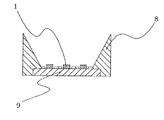
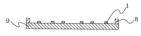
例えば、図3,図4に示す平面図,断面図のように複数個の発光装置1が発光装置駆動回路基板9に複数列に配置され、発光装置1の周囲に任意の形状に光学設計した反射治具8が設置されて成る照明装置の場合、隣接する一列上に配置された複数個の発光装置1において、隣り合う発光装置1との間隔が最短に成らないような配置、いわゆる千鳥状とすることが好ましい。即ち、発光装置1が格子状に配置される際には、光源となる発光装置1が直線上に配列されることによりグレアが強くなり、このような照明装置が人の視覚に入ってくることにより、不快感や目の障害を起こしやすくなるのに対し、千鳥状とすることにより、グレアが抑制され人間の目に対する不快感や目に及ぼす障害を低減することができる。さらに、隣り合う発光装置1間の距離が長くなることにより、隣接する発光装置1間の熱的な干渉が有効に抑制され、発光装置1が実装された発光装置駆動回路基板9内における熱のこもりが抑制され、発光装置1の外部に効率よく熱が放散される。その結果、人の目に対しても障害の小さい長期間にわたり光学特性の安定した長寿命の照明装置を作製することができる。
For example, a plurality of light emitting
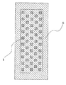
また、照明装置が、図5,図6に示す平面図,断面図のような発光装置駆動回路基板9上に複数の発光装置1から成る円状や多角形状の発光装置1群を、同心状に複数群形成した照明装置の場合、1つの円状や多角形状の発光装置1群における発光装置1の配置数を照明装置の中央側より外周側ほど多くすることが好ましい。これにより、発光装置1同士の間隔を適度に保ちながら発光装置1をより多く配置することができ、照明装置の照度をより向上させることができる。また、照明装置の中央部の発光装置1の密度を低くして発光装置駆動回路基板9の中央部における熱のこもりを抑制することができる。よって、発光装置駆動回路基板9内における温度分布が一様となり、照明装置を設置した外部電気回路基板やヒートシンクに効率よく熱が伝達され、発光装置1の温度上昇を抑制することができる。その結果、発光装置1は長期間にわたり安定して動作することができるとともに長寿命の照明装置を作製することができる。
Further, the lighting device is a concentric arrangement of a circular or polygonal light-emitting device group of a plurality of light-emitting
このような照明装置としては、例えば、室内や室外で用いられる、一般照明用器具、シャンデリア用照明器具、住宅用照明器具、オフィス用照明器具、店装,展示用照明器具、街路用照明器具、誘導灯器具及び信号装置、舞台及びスタジオ用の照明器具、広告灯、照明用ポール、水中照明用ライト、ストロボ用ライト、スポットライト、電柱等に埋め込む防犯用照明、非常用照明器具、懐中電灯、電光掲示板等や、調光器、自動点滅器、ディスプレイ等のバックライト、動画装置、装飾品、照光式スイッチ、光センサ、医療用ライト、車載ライト等が挙げられる。 Examples of such lighting devices include general lighting fixtures, chandelier lighting fixtures, residential lighting fixtures, office lighting fixtures, store lighting, display lighting fixtures, street lighting fixtures, used indoors and outdoors. Guide light fixtures and signaling devices, stage and studio lighting fixtures, advertising lights, lighting poles, underwater lighting lights, strobe lights, spotlights, security lights embedded in power poles, emergency lighting fixtures, flashlights, Examples include electronic bulletin boards and the like, backlights for dimmers, automatic flashers, displays and the like, moving image devices, ornaments, illuminated switches, optical sensors, medical lights, in-vehicle lights, and the like.
本発明の発光装置1について以下に実施例を示す。
Examples of the
まず、基体2となる種々の粒径の結晶粒から成るアルミナセラミックス基体を準備した。また、発光素子4が載置される載置部2aの周囲に、発光素子4と外部電気回路基板とを基体2の内部に形成した内部配線を介して電気的に接続するための配線導体を形成した。なお、基体2の上面の配線導体は、Mo−Mn粉末からなるメタライズ層により直径が0.1mmの円形パッドに成形されており、その表面に厚さ3μmのNiメッキ層と厚さ2μmのAuメッキ層とが順次被着されたものであった。また、基体2内部の内部配線は、貫通導体からなる電気接続部、いわゆるスルーホールによって形成された。このスルーホールについても配線導体と同様にMo−Mn粉末からなるメタライズ導体で成形された。
First, an alumina ceramic base made of crystal grains having various grain sizes to be the
次に、近紫外光を発する厚さ0.08mmの発光素子4を載置部2aにAgペーストで取着し、Auから成るボンディングワイヤを介して発光素子4を配線導体に電気的に接続した。
Next, the 0.08 mm thick light emitting element 4 emitting near ultraviolet light was attached to the mounting
次に、発光素子4の光によって励起され、黄色発光を行なう蛍光体を含有するシリコーン樹脂(透光性部材5)をディスペンサーによって、発光素子4の周囲に被覆し熱硬化させてサンプルとしての発光装置1を作製し光出力を測定した。
Next, a silicone resin (translucent member 5) containing a phosphor that emits yellow light by being excited by the light of the light emitting element 4 is coated around the light emitting element 4 by a dispenser and thermally cured to emit light as a sample. The
なお、蛍光体は、シリコーン樹脂に対して1/4の充填率(質量%)で均一に分散させた。また、蛍光体はその平均粒径が1.5乃至80μmでガーネット構造を有するイットリウム・アルミン酸塩系の黄色発光を行なう蛍光体を用いた。 The phosphor was uniformly dispersed at a filling rate (mass%) of 1/4 with respect to the silicone resin. The phosphor used was an yttrium-aluminate-based phosphor that has an average particle size of 1.5 to 80 μm and has a garnet structure.
基体2のセラミックスの結晶粒の平均粒径が10μm程度の場合、光出力が14mWであった。しかし、基体2のセラミックスの結晶粒の平均粒径が1乃至5μmの場合、光出力は17mWとなり、セラミックスの結晶粒の平均粒径が10μm程度と比して、光出力のエネルギーが20%以上増加した。即ち、セラミックスの結晶粒の平均粒径が10μm程度の場合に比し、セラミックスの結晶粒の平均粒径が1乃至5μmの基体を用いることにより、基体2の内部に入り込む光を有効に抑制するとともに基体2の表面における光散乱によって光照射される蛍光体の数が増加して光出力が向上したものと考えられる。
When the average grain size of the ceramic crystal grains of the
また、発光装置1の光出力を高めるために電流値を増加させた場合、セラミックスの平均粒径が1乃至5μmの基体の方が順方向電流に対する発光効率の低下を有効に抑制できたことも確認した。
In addition, when the current value is increased in order to increase the light output of the
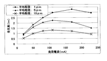
次に、上記の実施例と同一の構造でかつ基体2の焼結後におけるセラミックスの結晶粒の平均粒径が、1(μm)、5(μm)、10(μm)である発光装置1を作製し、発光素子4への負荷電流に対する全光束(光出力)を測定した。なお、発光装置1は、どちらも冷却性能が同等であるヒートシンクに実装され、光出力は積分球を用いて測定した。その結果を、図7に示す。
Next, the
図7より、発光素子4への負荷電流が定格電流である20(mA)、定格電圧が3.4(V)の場合、セラミックスの結晶粒の平均粒径が1(μm)である発光装置1の光出力は0.96(lm)となり、発光効率は14(lm/W)であった。また、セラミックスの結晶粒の平均粒径が5(μm)である発光装置1の光出力は0.8(lm)であり、発光効率は12(lm/W)であった。これに対して、セラミックスの結晶粒の平均粒径が10μmである発光装置1の光出力は0.55(lm)となり、発光効率は8(lm/W)であった。即ち、定格電流における発光装置1の光出力は、基体2のセラミックスの結晶粒の平均粒径が10(μm)と比べ、セラミックスの結晶粒の平均粒径が1(μm)、5(μm)である発光装置1の光出力は45乃至74(%)向上した。
From FIG. 7, when the load current to the light emitting element 4 is 20 (mA) as the rated current and the rated voltage is 3.4 (V), the average grain size of the ceramic crystal grains is 1 (μm). The light output was 0.96 (lm), and the light emission efficiency was 14 (lm / W). The light output of the light-emitting
即ち、基体2のセラミックスの結晶粒の平均粒径を1乃至5(μm)にすることにより、基体2の内部に入り込む光を有効に抑制するとともに、セラミックスの結晶粒によって基体2表面に形成される凹凸により、発光素子4より発せられた光が完全散乱に近い状態で反射する。従って、枠体3の内部に充填された蛍光体を均一な光強度で照射するとともに、光照射される蛍光体の数が増加することにより、発光素子4の光により励起される蛍光体の確率が上昇し、蛍光体の光変換効率が向上する。その結果、発光装置1は、基体2のセラミックスの結晶粒の平均粒径を1乃至5(μm)にすることにより、白熱灯の発光効率である12(lm/W)以上となり表示用や照明用の光源として実用化することができる。
That is, by making the average grain size of the ceramic crystal grains of the
また、発光装置1の光出力を向上させるために負荷電流を増加させた場合、基体2のセラミックスの結晶粒の平均粒径が大きい場合は、100(mA)よりも低い電流値付近で負荷電流に比例した光出力の上昇が見られなくなるのに対し、セラミックスの結晶粒の平均粒径を小さくすることにより、大きな電流値まで電流に比例して光出力が上昇し、特に平均粒径を1μmとすることによって発光装置1の光出力は110mA付近まで比例して上昇した。即ち、基体2のセラミックスの結晶粒の平均粒径を小さくすることにより、基体2内部の熱拡散性が向上し、発光素子4の負荷電流による温度上昇が抑制され、発光素子の発光効率の劣化を抑制することができる。
Further, when the load current is increased in order to improve the light output of the
さらにまた、発光装置1の負荷電流に対する発光素子4のピーク波長について、セラミックスの結晶粒の平均粒径を変えて発光装置1を作製し測定を行なったところ、基体2のセラミックスの結晶粒の平均粒径を1μmにすることにより、発光素子4のピーク波長の変動を小さくすることができることがわかった。これにより、発光素子4のピーク波長に依存する蛍光体の変換効率の変動を抑制することができる。さらに、発光装置1が、励起スペクトルの異なる複数の蛍光体から成る場合、発光素子4のピーク波長の変動によって生じる蛍光体の変換効率の変動が抑制される。その結果、複数の蛍光体からの励起光を混合して出力する発光装置1の光の色の変動が抑制される。例えば、蛍光体が赤色蛍光体、青色蛍光体、緑色蛍光体から成り、発光素子4のピーク波長が負荷電流により変動する場合、赤色蛍光体、青色蛍光体、緑色蛍光体の発光強度が、発光素子4のピーク波長によりそれぞれの特性で変動して発光装置1より出力される。即ち、赤色蛍光体、青色蛍光体、緑色蛍光体からの励起光の混合光における光強度の割合が変動し、出力光の色調が変動し、所望する色調の光が得られなくなる。従って、基体2のセラミックスの結晶粒の平均粒径を1μmにすることにより、発光素子4のピーク波長の変動が抑制され出力される光の色調の変動が抑制され、安定した発光特性かつ照明特性を有する照明用や表示用に適した発光装置を作製することができる。
Furthermore, the peak wavelength of the light-emitting element 4 with respect to the load current of the light-emitting
なお、本発明は以上の実施の形態の例および実施例に限定されず、本発明の要旨を逸脱しない範囲内で種々の変更を行なうことは何等支障ない。例えば、枠体3の上面に発光装置1より放出される光を任意に集光または拡散させることができる光学レンズや平板状の透光性の蓋体を半田や接着剤等で接合することにより、所望とする角度で光を取り出すことができるとともに発光装置1の内部への耐浸水性が改善され長期信頼性が向上する。また、枠体3の内周面は、その断面形状が平坦(直線状)または円弧状(曲線状)であってもよい。円弧状とする場合、発光素子4から発光される光を万遍なく反射させて指向性の高い光を外部に均一に放射することができる。また、光出力を高めるために基体2に発光素子4を複数設けても良い。さらに、枠体3の内周面の角度や、枠体3の上端から透光性部材5の上面までの距離を任意に調整することも可能であり、これにより、補色域を設けることによりさらに良好な演色性を得ることができる。
It should be noted that the present invention is not limited to the above-described embodiments and examples, and various modifications can be made without departing from the scope of the present invention. For example, by bonding an optical lens capable of arbitrarily collecting or diffusing light emitted from the
また、本発明の照明装置は、複数個の発光装置1を所定の配置となるように設置したものだけでなく、1個の発光装置1を所定の配置となるように設置したものでもよい。
Further, the lighting device of the present invention is not limited to one in which a plurality of light emitting
1:発光装置
2:基体
2a:載置部
3:枠体
4:発光素子
5:透光性部材
6:発光部
8:反射治具
9:発光装置駆動回路基板
1: Light-emitting device 2:
Claims (4)
Priority Applications (7)
| Application Number | Priority Date | Filing Date | Title |
|---|---|---|---|
| JP2004275058A JP2005294796A (en) | 2003-12-19 | 2004-09-22 | Light emitting element storage package, light emitting device, and lighting device |
| US10/978,302 US20050133808A1 (en) | 2003-09-11 | 2004-10-29 | Package for housing light-emitting element, light-emitting apparatus and illumination apparatus |
| TW093133106A TWI245436B (en) | 2003-10-30 | 2004-10-29 | Package for housing light-emitting element, light-emitting apparatus and illumination apparatus |
| KR1020040087566A KR20050041986A (en) | 2003-10-30 | 2004-10-30 | Package for housing light-emitting element, light-emitting apparatus and illumination apparatus |
| CNB2004100900711A CN100392877C (en) | 2003-10-30 | 2004-11-01 | Package for storing light-emitting element, light-emitting device, and lighting device |
| DE102004052902A DE102004052902B4 (en) | 2003-10-30 | 2004-11-02 | A structure for housing a light-emitting element, light-emitting device and lighting device |
| KR1020060069330A KR20060107428A (en) | 2003-10-30 | 2006-07-24 | Light emitting device |
Applications Claiming Priority (3)
| Application Number | Priority Date | Filing Date | Title |
|---|---|---|---|
| JP2003423439 | 2003-12-19 | ||
| JP2004071428 | 2004-03-12 | ||
| JP2004275058A JP2005294796A (en) | 2003-12-19 | 2004-09-22 | Light emitting element storage package, light emitting device, and lighting device |
Related Child Applications (1)
| Application Number | Title | Priority Date | Filing Date |
|---|---|---|---|
| JP2006149683A Division JP2006270120A (en) | 2003-12-19 | 2006-05-30 | Light emitting diode device |
Publications (2)
| Publication Number | Publication Date |
|---|---|
| JP2005294796A true JP2005294796A (en) | 2005-10-20 |
| JP2005294796A5 JP2005294796A5 (en) | 2006-09-07 |
Family
ID=35327339
Family Applications (1)
| Application Number | Title | Priority Date | Filing Date |
|---|---|---|---|
| JP2004275058A Pending JP2005294796A (en) | 2003-09-11 | 2004-09-22 | Light emitting element storage package, light emitting device, and lighting device |
Country Status (1)
| Country | Link |
|---|---|
| JP (1) | JP2005294796A (en) |
Cited By (4)
| Publication number | Priority date | Publication date | Assignee | Title |
|---|---|---|---|---|
| JP2010087224A (en) * | 2008-09-30 | 2010-04-15 | Toyoda Gosei Co Ltd | Led display device and method of manufacturing barrier for led display device |
| EP1953836A4 (en) * | 2005-11-21 | 2013-10-23 | Nippon Carbide Kogyo Kk | REFLECTIVE MATERIAL, LIGHT EMITTING ELEMENT HOUSING PACKAGE, LIGHT EMITTING DEVICE, AND LIGHT EMITTING ELEMENT HOUSING PACKAGE PROCESS |
| JP2014225022A (en) * | 2014-06-18 | 2014-12-04 | 株式会社東芝 | Illumination device, imaging device, and portable terminal |
| JP2016170349A (en) * | 2015-03-13 | 2016-09-23 | セイコーエプソン株式会社 | Wavelength conversion element, light source device, projector and method for producing wavelength conversion element |
Citations (4)
| Publication number | Priority date | Publication date | Assignee | Title |
|---|---|---|---|---|
| JPH0196067A (en) * | 1987-10-08 | 1989-04-14 | Nec Corp | Production of aluminum nitride sintered body |
| JPH059836A (en) * | 1991-07-09 | 1993-01-19 | Kuraray Co Ltd | Shade curtain for vehicle |
| JP2002234774A (en) * | 2000-12-04 | 2002-08-23 | Sumitomo Electric Ind Ltd | Ceramic optical component and method of manufacturing the same |
| JP2003347600A (en) * | 2002-05-28 | 2003-12-05 | Matsushita Electric Works Ltd | LED mounting board |
-
2004
- 2004-09-22 JP JP2004275058A patent/JP2005294796A/en active Pending
Patent Citations (4)
| Publication number | Priority date | Publication date | Assignee | Title |
|---|---|---|---|---|
| JPH0196067A (en) * | 1987-10-08 | 1989-04-14 | Nec Corp | Production of aluminum nitride sintered body |
| JPH059836A (en) * | 1991-07-09 | 1993-01-19 | Kuraray Co Ltd | Shade curtain for vehicle |
| JP2002234774A (en) * | 2000-12-04 | 2002-08-23 | Sumitomo Electric Ind Ltd | Ceramic optical component and method of manufacturing the same |
| JP2003347600A (en) * | 2002-05-28 | 2003-12-05 | Matsushita Electric Works Ltd | LED mounting board |
Cited By (4)
| Publication number | Priority date | Publication date | Assignee | Title |
|---|---|---|---|---|
| EP1953836A4 (en) * | 2005-11-21 | 2013-10-23 | Nippon Carbide Kogyo Kk | REFLECTIVE MATERIAL, LIGHT EMITTING ELEMENT HOUSING PACKAGE, LIGHT EMITTING DEVICE, AND LIGHT EMITTING ELEMENT HOUSING PACKAGE PROCESS |
| JP2010087224A (en) * | 2008-09-30 | 2010-04-15 | Toyoda Gosei Co Ltd | Led display device and method of manufacturing barrier for led display device |
| JP2014225022A (en) * | 2014-06-18 | 2014-12-04 | 株式会社東芝 | Illumination device, imaging device, and portable terminal |
| JP2016170349A (en) * | 2015-03-13 | 2016-09-23 | セイコーエプソン株式会社 | Wavelength conversion element, light source device, projector and method for producing wavelength conversion element |
Similar Documents
| Publication | Publication Date | Title |
|---|---|---|
| JP5196711B2 (en) | LIGHT EMITTING DEVICE AND LIGHTING DEVICE USING THE SAME | |
| US7192164B2 (en) | Light-emitting apparatus and illuminating apparatus | |
| JP2006237264A (en) | Light emitting device and lighting device | |
| JP4143043B2 (en) | Light emitting device and lighting device | |
| JP3921474B2 (en) | Light emitting device and lighting device | |
| JP2005159262A (en) | Light emitting element storage package, light emitting device, and lighting device | |
| JP3898721B2 (en) | Light emitting device and lighting device | |
| JP2006066657A (en) | Light emitting device and lighting device | |
| JP2005210042A (en) | Light emitting device and lighting device | |
| JP2006093399A (en) | LIGHT EMITTING DEVICE, ITS MANUFACTURING METHOD, AND LIGHTING DEVICE | |
| JP2005277331A (en) | Light emitting device and lighting device | |
| JP2006049814A (en) | Light emitting device and lighting device | |
| JP4671745B2 (en) | LIGHT EMITTING DEVICE AND LIGHTING DEVICE USING THE SAME | |
| JP2006210627A (en) | Light emitting element storage package, light emitting device, and lighting device | |
| JP2006100441A (en) | Light emitting element storage package, light emitting device, and lighting device | |
| JP4845370B2 (en) | Light emitting device and lighting device | |
| JP2007266358A (en) | Light emitting device and lighting device | |
| JP2005310911A (en) | Light emitting element storage package, light emitting device, and lighting device | |
| JP4624069B2 (en) | LIGHT EMITTING DEVICE, ITS MANUFACTURING METHOD, AND LIGHTING DEVICE | |
| JP4511238B2 (en) | Light emitting element storage package, light emitting device, and lighting device | |
| JP2007201334A (en) | Light emitting device and lighting device | |
| JP2006295230A (en) | Light emitting device and lighting device | |
| JP2005183899A (en) | Light emitting element storage package, light emitting device, and lighting device | |
| JP2006093612A (en) | Light emitting device and lighting device | |
| JP2005294796A (en) | Light emitting element storage package, light emitting device, and lighting device |
Legal Events
| Date | Code | Title | Description |
|---|---|---|---|
| A521 | Written amendment |
Free format text: JAPANESE INTERMEDIATE CODE: A523 Effective date: 20060725 |
|
| A871 | Explanation of circumstances concerning accelerated examination |
Free format text: JAPANESE INTERMEDIATE CODE: A871 Effective date: 20060725 |
|
| A975 | Report on accelerated examination |
Free format text: JAPANESE INTERMEDIATE CODE: A971005 Effective date: 20060810 |
|
| A131 | Notification of reasons for refusal |
Free format text: JAPANESE INTERMEDIATE CODE: A131 Effective date: 20060926 |
|
| A521 | Written amendment |
Free format text: JAPANESE INTERMEDIATE CODE: A523 Effective date: 20061127 |
|
| A02 | Decision of refusal |
Free format text: JAPANESE INTERMEDIATE CODE: A02 Effective date: 20061226 |