JP2005292835A - パターン化グリッドエレメント偏光器 - Google Patents
パターン化グリッドエレメント偏光器 Download PDFInfo
- Publication number
- JP2005292835A JP2005292835A JP2005103166A JP2005103166A JP2005292835A JP 2005292835 A JP2005292835 A JP 2005292835A JP 2005103166 A JP2005103166 A JP 2005103166A JP 2005103166 A JP2005103166 A JP 2005103166A JP 2005292835 A JP2005292835 A JP 2005292835A
- Authority
- JP
- Japan
- Prior art keywords
- polarizer
- light
- elements
- substrate
- ultraviolet
- Prior art date
- Legal status (The legal status is an assumption and is not a legal conclusion. Google has not performed a legal analysis and makes no representation as to the accuracy of the status listed.)
- Granted
Links
Images
Classifications
-
- G—PHYSICS
- G02—OPTICS
- G02B—OPTICAL ELEMENTS, SYSTEMS OR APPARATUS
- G02B5/00—Optical elements other than lenses
- G02B5/30—Polarising elements
- G02B5/3025—Polarisers, i.e. arrangements capable of producing a definite output polarisation state from an unpolarised input state
- G02B5/3075—Polarisers, i.e. arrangements capable of producing a definite output polarisation state from an unpolarised input state for use in the UV
-
- G—PHYSICS
- G02—OPTICS
- G02B—OPTICAL ELEMENTS, SYSTEMS OR APPARATUS
- G02B27/00—Optical systems or apparatus not provided for by any of the groups G02B1/00 - G02B26/00, G02B30/00
- G02B27/28—Optical systems or apparatus not provided for by any of the groups G02B1/00 - G02B26/00, G02B30/00 for polarising
- G02B27/286—Optical systems or apparatus not provided for by any of the groups G02B1/00 - G02B26/00, G02B30/00 for polarising for controlling or changing the state of polarisation, e.g. transforming one polarisation state into another
-
- G—PHYSICS
- G02—OPTICS
- G02B—OPTICAL ELEMENTS, SYSTEMS OR APPARATUS
- G02B5/00—Optical elements other than lenses
- G02B5/30—Polarising elements
- G02B5/3025—Polarisers, i.e. arrangements capable of producing a definite output polarisation state from an unpolarised input state
- G02B5/3058—Polarisers, i.e. arrangements capable of producing a definite output polarisation state from an unpolarised input state comprising electrically conductive elements, e.g. wire grids, conductive particles
-
- G—PHYSICS
- G03—PHOTOGRAPHY; CINEMATOGRAPHY; ANALOGOUS TECHNIQUES USING WAVES OTHER THAN OPTICAL WAVES; ELECTROGRAPHY; HOLOGRAPHY
- G03F—PHOTOMECHANICAL PRODUCTION OF TEXTURED OR PATTERNED SURFACES, e.g. FOR PRINTING, FOR PROCESSING OF SEMICONDUCTOR DEVICES; MATERIALS THEREFOR; ORIGINALS THEREFOR; APPARATUS SPECIALLY ADAPTED THEREFOR
- G03F7/00—Photomechanical, e.g. photolithographic, production of textured or patterned surfaces, e.g. printing surfaces; Materials therefor, e.g. comprising photoresists; Apparatus specially adapted therefor
- G03F7/70—Microphotolithographic exposure; Apparatus therefor
- G03F7/70483—Information management; Active and passive control; Testing; Wafer monitoring, e.g. pattern monitoring
- G03F7/7055—Exposure light control in all parts of the microlithographic apparatus, e.g. pulse length control or light interruption
- G03F7/70566—Polarisation control
-
- H—ELECTRICITY
- H10—SEMICONDUCTOR DEVICES; ELECTRIC SOLID-STATE DEVICES NOT OTHERWISE PROVIDED FOR
- H10P—GENERIC PROCESSES OR APPARATUS FOR THE MANUFACTURE OR TREATMENT OF DEVICES COVERED BY CLASS H10
- H10P76/00—Manufacture or treatment of masks on semiconductor bodies, e.g. by lithography or photolithography
Landscapes
- Physics & Mathematics (AREA)
- General Physics & Mathematics (AREA)
- Optics & Photonics (AREA)
- Polarising Elements (AREA)
- Exposure Of Semiconductors, Excluding Electron Or Ion Beam Exposure (AREA)
- Exposure And Positioning Against Photoresist Photosensitive Materials (AREA)
Abstract
【解決手段】リソグラフで使用するためのパターン化グリッド偏光器において、
(a)紫外線(UV)光に対して透明な基板と、
(b)該基板上にパターン化されたエレメントのアレイを有し、
該エレメントは紫外線光を偏光する、ことを特徴とする偏光器。
【選択図】図1
Description
もっとも簡単なグリッドエレメント偏光器は、平行な導電ワイヤのグリッドからなるデバイスである。光がグリッドに入射すると、照射の各直交成分はワイヤグリッド偏光器とそれぞれ異なって交差する。ワイヤに平行なフィールドの成分は電子を各ワイヤの長手方向に沿ってドライブし、これにより電流が発生する。電子はまた格子原子と衝突し、エネルギーをこれに付与し、これによりワイヤを加熱する。このようにしてエネルギーはフィールドからグリッドに伝達される。さらにワイヤに平行に加速する電子は前方向と後方向の両方に放射する。入射波は前方向に放射される波により相殺される傾向にあり、そのためフィールドのその成分は透過しないか、またはほとんど透過しない。後方向に伝播する放射は単純に反射波として現れる。反対に、ワイヤに垂直の波の成分は実質的に変化せずグリッドを通過して伝播する。(Eugene Hecht, Optics, Chapter 8, pp.333-334, Addison Wesley, San Francisco(2002))
1960年にGeorge R. BirdとMaxfield Parish, Jr.は1mm当たりに2160本のワイヤを有する、マイクロ波領域で使用するためのグリッド偏光器を開示している(G.R. BirdとM. Parish,Jr.,J. Opt. Soc. Am. 50:886(1960))。この刊行物によれば、このことは金(またはアルミニウム)原子流を密な入射角でプラスチックの回折格子レプリカに蒸着させることにより達成された。回折格子の各ステップのエッジに沿って堆積する金属は薄い顕微鏡的ワイヤを形成し、このワイヤの幅と間隔は波長よりも小さい。
より高速にかつより精巧な回路を形成するために、半導体製造業は回路素子の大きさを低減する努力を続けている。回路は基本的にフォトリソグラフにより製造される。このプロセスで、回路は半導体ウェハの上に、感光性材料のコーティングを光に露光することによってプリントされる。感光性材料はしばしば「フォトレジスト」またはレジストと称される。クロムまたは他の不透明材料からなるマスクを、透明基板上に形成する。光をこのマスクに通過させると所望の回路パターンが発生する。このマスクはまた、透明基板の表面にエッチングされた比較的高い領域と比較的低い領域のパターンにより形成することもできる。またはこれら2つの技術を組み合わせることもできる。引き続き、熱的または化学的プロセスによりこのレジストの露光された部分または露光されなかった部分(材料に依存する)だけを除去し、露出された基板領域を残す。この領域がさらなるプロセスでは電子回路の製造に使用される。
本発明は、さまざまな手法で基板上にパターン化されたエレメントを備えるUV偏光器を提供する。本発明では、基板上のエレメントのパターンが偏光器を出射する光の偏光を規定するように構成されている。
本発明の実施例では、エレメントが基板上にパターン化されており、導電材料、例えば金属から形成される。エレメントは例えばアルミニウム、銀または金から形成することができる。このようなエレメントは制限されるものではないが、ワイヤまたはマイクロワイヤを含む。
本発明はさらに本発明の偏光器を使用する装置を提供する。例えば本発明の偏光器は紫外線光を偏光するための装置に使用することができる。このような装置は例えば紫外線スペクトル中に少なくとも1つの波長を有する光ビームを形成する光源を有し、さらに基板を有し、この基板は紫外線スペクトルにある光に対して透明であり、光ビーム路に配置されており、さらに基板上にリソグラフでエッチングされたエレメントアレイを有する。ここで基板上にリソグラフでエッチングされたエレメントアレイは偏光された出射光を形成する。
導電性エレメントのアレイを基板上に配置することは、複数の周知技術により実行することができる。例えば米国特許第4049944号および米国特許第4514479号には、ホログラム干渉リソグラフを使用して、微細な格子構造をフォトレジストに形成し、続いてイオンビームによりエッチングしてこの構造体を基礎となる金属フィルムに変換することが記載されている。Stenkampは(“Grid polarizer for the visible spectral region”, Proceedings of the SPIE, vol.2213, pp.288-296)、ダイレクトe-beamリソグラフを使用してレジストパターンを形成し、続いてリアクティブイオンエッチングによりパターンを金属フィルムに変換することを開示している。極紫外線リソグラフおよびX線リソグラフ、X線ホログラム干渉リソグラフを含む他の高解像度リソグラス技術もレジストパターンを形成するに使用することができる。他のエッチングメカニズムおよびリフトオフプロセスを含む他の技術もパターンをレジストから金属フィルムに変換するのに使用することができる。導電性エレメントのアレイを形成するために使用される正確なプロセスは本発明に対しては重要でない。
Claims (27)
- リソグラフで使用するためのパターン化グリッド偏光器において、
(a)紫外線(UV)光に対して透明な基板と、
(b)該基板上にパターン化されたエレメントのアレイを有し、
該エレメントは紫外線光を偏光する、ことを特徴とする偏光器。 - 請求項1記載の偏光器において、パターン化されたエレメントは接線方向に偏光された出射光を、非偏光の入射光から形成し、
該入射光は偏光器に入射し、出射光を偏光器から出射する。 - 請求項1記載の偏光器において、パターン化されたエレメントは半径方向に偏光された出射光を、非偏光の入射光から形成し、
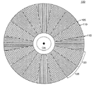
該入射光は偏光器に入射し、出射光を偏光器から出射する。 - 請求項1記載の偏光器において、エレメントは複数の群にパターン化されており、
該群は円形パターンに配置されており、
各群は平行なエレメントからなり、
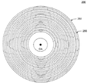
第1の群のエレメントは第2の群のエレメントに対して平行ではない。 - 請求項1記載の偏光器において、エレメントは円形である。
- 請求項5記載の偏光器において、エレメントは同心円にパターン化されている。
- 請求項1記載の偏光器において、エレメントは、紫外線光の波長の約1/10から紫外線光の波長の2倍の間のピッチを有する。
- 請求項1記載の偏光器において、エレメントは紫外線光の波長の約1/4のピッチを有する。
- 請求項1記載の偏光器において、エレメントは約45nmから95nmの間の周期を有する。
- 請求項1記載の偏光器において、エレメントは近似的に0.04μmから0.3μmの間の厚さを有する。
- 請求項1記載の偏光器において、エレメントはアルミニウム、銀または金を含む。
- 請求項1記載の偏光器において、さらに紫外線光源を有する。
- 請求項12記載の偏光器において、紫外線光は偏光されていない。
- 請求項12記載の偏光器において、紫外線光は少なくとも2つの偏光方向を有し、
ワイヤグリッド偏光器は第1の偏光方向の光の大部分を反射し、第2の偏光方向の光の大部分を透過する。 - 請求項12記載の偏光器において、ワイヤグリッド偏光器は紫外線光を接線方向に偏光された光に変換する。
- 請求項12記載の偏光器において、ワイヤグリッド偏光器は紫外線光を半径方向に偏光された光に変換する。
- 請求項1記載の偏光器において、基板は石英ガラス、フッ化カルシウム、サファイヤ、水晶またはフッ化マグネシウムである。
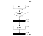
- 紫外線光を偏光するための装置であって、
(a)紫外線スペクトル中に少なくとも1つの波長を有する光ビームを形成する光源と、
(b)紫外線スペクトルの光に対して透明であり、光ビームの経路に配置された基板と、
(c)基板上にあるエレメントのアレイと、
を有する装置において、
エレメントのアレイは入射紫外線光を偏光し、偏光された光を出射する、ことを特徴とする装置。 - 請求項18記載の装置において、エレメントは紫外線光ビームの波長の約1/4の周期を有する。
- 請求項18記載の装置において、エレメントは約0.1λと0.5λの間の周期を有し、ここでλはビームの波長である。
- 請求項18記載の装置において、エレメントの厚さは0.04μmから0.3μmの間である。
- 請求項18記載の装置において、基板は石英ガラス、フッ化カルシウム、またはサファイヤを含む。
- 請求項18記載の装置において、エレメントは一般的に第1偏光方向の入射光の大部分を反射し、第2偏光方向の光の大部分を透過する。
- 請求項18記載の装置において、エレメントは接線方向に偏光された出射光を形成するように放射状に構成されている。
- 請求項18記載の装置において、エレメントは半径方向に偏光された光を形成するように同心円に構成されている。
- 光経路に沿って露光ビームを形成するための装置であって、
(a)ワイヤグリッド偏光器と、
(b)瞳を備える照明器と、
を有する形式の装置において、
偏光器は、紫外線(UV)光に対して透明な基板と、基板上にパターン化されたエレメントのアレイを有し、該エレメントは紫外線光を偏光し、偏光パターンを紫外線光中に照明器の瞳で形成する、ことを特徴とする装置。 - 光経路に沿って露光ビームを形成するための装置であって、
(a)ワイヤグリッド偏光器と、
(b)投影光学系と、
を有する形式の装置において、
偏光器は、紫外線(UV)光に対して透明な基板と、基板上にパターン化されたエレメントのアレイを有し、該エレメントは紫外線光を偏光し、偏光パターンを投影光学系に向かう紫外線光出力中に形成する、ことを特徴とする装置。
Applications Claiming Priority (1)
| Application Number | Priority Date | Filing Date | Title |
|---|---|---|---|
| US10/813,168 US7304719B2 (en) | 2004-03-31 | 2004-03-31 | Patterned grid element polarizer |
Publications (2)
| Publication Number | Publication Date |
|---|---|
| JP2005292835A true JP2005292835A (ja) | 2005-10-20 |
| JP4264071B2 JP4264071B2 (ja) | 2009-05-13 |
Family
ID=34887695
Family Applications (1)
| Application Number | Title | Priority Date | Filing Date |
|---|---|---|---|
| JP2005103166A Expired - Fee Related JP4264071B2 (ja) | 2004-03-31 | 2005-03-31 | リソグラフィ装置 |
Country Status (7)
| Country | Link |
|---|---|
| US (1) | US7304719B2 (ja) |
| EP (1) | EP1582894B1 (ja) |
| JP (1) | JP4264071B2 (ja) |
| KR (1) | KR100664623B1 (ja) |
| CN (1) | CN100388026C (ja) |
| SG (1) | SG115821A1 (ja) |
| TW (1) | TWI305279B (ja) |
Cited By (5)
| Publication number | Priority date | Publication date | Assignee | Title |
|---|---|---|---|---|
| JP2007128086A (ja) * | 2005-10-31 | 2007-05-24 | Toshiba Corp | 短波長用偏光素子及び偏光素子製造方法 |
| JP2007128087A (ja) * | 2005-10-31 | 2007-05-24 | Toshiba Corp | 短波長用偏光素子及び偏光素子製造方法 |
| JP2010134411A (ja) * | 2008-11-07 | 2010-06-17 | Ricoh Co Ltd | 偏光分離デバイス、偏光分離素子の製造方法、光走査装置及び画像形成装置 |
| KR20110133571A (ko) * | 2009-03-03 | 2011-12-13 | 인터내셔널 비지네스 머신즈 코포레이션 | 광학 리소그래피 장치 |
| WO2025164595A1 (ja) * | 2024-01-29 | 2025-08-07 | 株式会社フォトニックラティス | 光配向露光用の偏光マスク、光配向露光方法、及び光学部品等の製造方法 |
Families Citing this family (58)
| Publication number | Priority date | Publication date | Assignee | Title |
|---|---|---|---|---|
| US20070019179A1 (en) | 2004-01-16 | 2007-01-25 | Damian Fiolka | Polarization-modulating optical element |
| US8270077B2 (en) | 2004-01-16 | 2012-09-18 | Carl Zeiss Smt Gmbh | Polarization-modulating optical element |
| CN101799587B (zh) | 2004-01-16 | 2012-05-30 | 卡尔蔡司Smt有限责任公司 | 光学系统、投影系统及微结构半导体部件的制造方法 |
| JP4451268B2 (ja) * | 2004-03-04 | 2010-04-14 | 株式会社リコー | 光学素子及びその製造方法と、これを用いた光学製品、光ピックアップ及び光情報処理装置 |
| US7304719B2 (en) | 2004-03-31 | 2007-12-04 | Asml Holding N.V. | Patterned grid element polarizer |
| US7324280B2 (en) | 2004-05-25 | 2008-01-29 | Asml Holding N.V. | Apparatus for providing a pattern of polarization |
| US7548370B2 (en) * | 2004-06-29 | 2009-06-16 | Asml Holding N.V. | Layered structure for a tile wave plate assembly |
| DE102004040534B4 (de) * | 2004-08-20 | 2006-06-14 | Carl Zeiss Jena Gmbh | Diffraktives polarisationstrennendes Element für unpolarisierte elektromagnetische Strahlung im UV-Bereich, System mit zwei solchen Elementen und Verfahren zur Herstellung eines solchen Elementes |
| JP4479535B2 (ja) * | 2005-02-21 | 2010-06-09 | セイコーエプソン株式会社 | 光学素子の製造方法 |
| DE102006032810A1 (de) | 2006-07-14 | 2008-01-17 | Carl Zeiss Smt Ag | Beleuchtungsoptik für eine Mikrolithografie-Projektionsbelichtungsanlage, Beleuchtungssystem mit einer derartigen Beleuchtungsoptik, mikrolithografie-Projektionsbelichtungsanlage mit einem derartigen Beleuchtungssystem, mikrolithografisches Herstellungsverfahren für Bauelemente sowie mit diesem Verfahren hergestelltes Bauelement |
| TWI307677B (en) * | 2006-07-18 | 2009-03-21 | Applied Res Lab | Method and device for fabricating nano-structure with patterned particle beam |
| US8792161B2 (en) * | 2007-02-21 | 2014-07-29 | Globalfoundries Inc. | Optical polarizer with nanotube array |
| US7777943B2 (en) * | 2007-03-01 | 2010-08-17 | American Museum Of Natural History | Astrometry and photometry with coronagraphs |
| US8643822B2 (en) * | 2007-07-03 | 2014-02-04 | Jds Uniphase Corporation | Non-etched flat polarization-selective diffractive optical elements |
| DE102008002749A1 (de) * | 2008-06-27 | 2009-12-31 | Carl Zeiss Smt Ag | Beleuchtungsoptik für die Mikrolithografie |
| JP2011013654A (ja) * | 2008-10-23 | 2011-01-20 | Seiko Epson Corp | 多層反射防止層およびその製造方法、プラスチックレンズ |
| JP2010197352A (ja) * | 2009-02-27 | 2010-09-09 | Hitachi High-Technologies Corp | 欠陥検査方法及び欠陥検査装置 |
| JP2010231171A (ja) * | 2009-03-04 | 2010-10-14 | Seiko Epson Corp | 光学物品およびその製造方法 |
| JP2010231172A (ja) * | 2009-03-04 | 2010-10-14 | Seiko Epson Corp | 光学物品およびその製造方法 |
| JP2011053660A (ja) * | 2009-08-05 | 2011-03-17 | Hoya Corp | 偏光レンズ |
| JP5588135B2 (ja) * | 2009-08-10 | 2014-09-10 | ホーヤ レンズ マニュファクチャリング フィリピン インク | 光学物品の製造方法 |
| JP5523066B2 (ja) * | 2009-11-17 | 2014-06-18 | ホーヤ レンズ マニュファクチャリング フィリピン インク | 光学物品の製造方法 |
| US10274650B2 (en) | 2010-01-29 | 2019-04-30 | Beam Engineering For Advanced Measurements Co. | Diffractive waveplate lenses and applications |
| US11366254B2 (en) | 2010-01-29 | 2022-06-21 | Beam Engineering For Advanced Measurements Co. | High-efficiency wide-angle beam steering system |
| US9557456B2 (en) | 2010-01-29 | 2017-01-31 | The United States Of America As Represented By The Secretary Of The Army | Broadband optics for manipulating light beams and images |
| US10114239B2 (en) | 2010-04-21 | 2018-10-30 | Beam Engineering For Advanced Measurements Co. | Waveplate lenses and methods for their fabrication |
| US9983479B2 (en) * | 2010-04-21 | 2018-05-29 | Beam Engineering For Advanced Measurements Co. | Fabrication of high efficiency, high quality, large area diffractive waveplates and arrays |
| US10197715B1 (en) | 2013-03-15 | 2019-02-05 | Beam Engineering For Advanced Measurements Co. | Methods of diffractive lens and mirror fabrication |
| US20110262844A1 (en) | 2010-04-21 | 2011-10-27 | Beam Engineering For Advanced Measurement Co. | Fabrication of high efficiency, high quality, large area diffractive waveplates and arrays |
| US8625107B2 (en) * | 2010-05-19 | 2014-01-07 | Uwm Research Foundation, Inc. | Target for motion tracking system |
| CN101938080B (zh) * | 2010-06-25 | 2011-11-30 | 北京交通大学 | 一种具有单模输出tm01模式特性的有源光纤 |
| JP2012032690A (ja) | 2010-08-02 | 2012-02-16 | Seiko Epson Corp | 光学物品およびその製造方法 |
| CN102722034B (zh) * | 2012-02-11 | 2015-10-07 | 深圳市光峰光电技术有限公司 | 偏振分光装置及相关光源 |
| DE102012205554A1 (de) * | 2012-04-04 | 2013-04-25 | Carl Zeiss Smt Gmbh | Optisches System für die Mikrolithographie |
| DE102012206151A1 (de) * | 2012-04-16 | 2013-05-02 | Carl Zeiss Smt Gmbh | Optisches System, insbesondere einer mikrolithographischen Projektionsbelichtungsanlage |
| DE102013202590A1 (de) * | 2013-02-19 | 2014-09-04 | Carl Zeiss Smt Gmbh | EUV-Lichtquelle zur Erzeugung eines Nutz-Ausgabestrahls für eine Projektionsbelichtungsanlage |
| US10107945B2 (en) | 2013-03-01 | 2018-10-23 | Beam Engineering For Advanced Measurements Co. | Vector vortex waveplates |
| US10185182B2 (en) * | 2013-03-03 | 2019-01-22 | Beam Engineering For Advanced Measurements Co. | Mechanical rubbing method for fabricating cycloidal diffractive waveplates |
| DE102013207502A1 (de) | 2013-04-25 | 2014-05-15 | Carl Zeiss Smt Gmbh | Optisches System, insbesondere für eine Wafer- oder Maskeninspektionsanlage |
| DE102013209042A1 (de) | 2013-05-15 | 2014-05-08 | Carl Zeiss Smt Gmbh | Optisches System einer mikrolithographischen Projektionsbelichtungsanlage |
| CA2941274C (en) | 2014-03-04 | 2020-02-25 | Novadaq Technologies Inc. | Spatial and spectral filtering apertures and optical imaging systems including the same |
| CN106605164B (zh) | 2014-03-04 | 2020-04-24 | 诺瓦达克技术公司 | 用于宽带成像的中继透镜系统 |
| KR102413901B1 (ko) * | 2015-04-24 | 2022-06-28 | 삼성디스플레이 주식회사 | 와이어 그리드 편광판 및 이를 포함하는 표시장치 |
| US9976911B1 (en) | 2015-06-30 | 2018-05-22 | Beam Engineering For Advanced Measurements Co. | Full characterization wavefront sensor |
| US10191296B1 (en) | 2015-06-30 | 2019-01-29 | Beam Engineering For Advanced Measurements Co. | Laser pointer with reduced risk of eye injury |
| KR102427155B1 (ko) * | 2015-08-25 | 2022-07-29 | 삼성디스플레이 주식회사 | 레이저 결정화 장치 |
| CN108431649B (zh) | 2015-08-31 | 2021-08-24 | 史赛克欧洲运营有限公司 | 偏振依赖滤波器、使用其的系统以及相关联的工具包和方法 |
| US10436957B2 (en) | 2015-10-27 | 2019-10-08 | Beam Engineering For Advanced Measurements Co. | Broadband imaging with diffractive waveplate coated mirrors and diffractive waveplate objective lens |
| WO2017151291A1 (en) * | 2016-03-04 | 2017-09-08 | Applied Materials, Inc. | Wire grid polarizer manufacturing method |
| EP3270237B1 (fr) * | 2016-07-13 | 2018-11-07 | The Swatch Group Research and Development Ltd. | Objet portable comprenant un dispositif d'affichage d'au moins une information vue à travers une lame retard |
| US10423045B2 (en) | 2016-11-14 | 2019-09-24 | Beam Engineering For Advanced Measurements Co. | Electro-optical diffractive waveplate beam shaping system |
| KR101852071B1 (ko) * | 2016-12-28 | 2018-04-26 | 한국과학기술연구원 | 전자기파 필터를 위한 메타물질 |
| US10274805B2 (en) | 2017-06-13 | 2019-04-30 | Beam Engineering For Advanced Measurements Co. | Polarization-independent switchable lens system |
| US11175441B1 (en) | 2018-03-05 | 2021-11-16 | Beam Engineering For Advanced Measurements Co. | Polarization-independent diffractive optical structures |
| US11982906B1 (en) | 2018-03-05 | 2024-05-14 | Beam Engineering For Advanced Measurements Co. | Polarization-independent diffractive optical structures |
| CN109254341A (zh) * | 2018-10-31 | 2019-01-22 | 南京奥谱依电子科技有限公司 | 一种图案化控偏膜片及其制备方法 |
| CN111239878A (zh) * | 2018-11-09 | 2020-06-05 | 英属开曼群岛商音飞光电科技股份有限公司 | 光栅板装置 |
| US11294240B2 (en) | 2019-08-10 | 2022-04-05 | Beam Engineering For Advanced Measurements Co. | Diffractive waveplate devices that operate over a wide temperature range |
Family Cites Families (32)
| Publication number | Priority date | Publication date | Assignee | Title |
|---|---|---|---|---|
| US3719415A (en) * | 1971-09-22 | 1973-03-06 | Bell Telephone Labor Inc | Radial and tangential polarizers |
| US3877789A (en) * | 1972-11-08 | 1975-04-15 | Marie G R P | Mode transformer for light or millimeter electromagnetic waves |
| US4049944A (en) | 1973-02-28 | 1977-09-20 | Hughes Aircraft Company | Process for fabricating small geometry semiconductive devices including integrated components |
| US4514479A (en) | 1980-07-01 | 1985-04-30 | The United States Of America As Represented By The Secretary Of The Navy | Method of making near infrared polarizers |
| JP2796005B2 (ja) | 1992-02-10 | 1998-09-10 | 三菱電機株式会社 | 投影露光装置及び偏光子 |
| JPH05307112A (ja) * | 1992-04-28 | 1993-11-19 | Satoyuki Saito | 偏光板 |
| JPH08184711A (ja) | 1994-12-29 | 1996-07-16 | Sony Corp | 偏光光学素子 |
| DE19535392A1 (de) | 1995-09-23 | 1997-03-27 | Zeiss Carl Fa | Radial polarisationsdrehende optische Anordnung und Mikrolithographie-Projektionsbelichtungsanlage damit |
| KR0171947B1 (ko) * | 1995-12-08 | 1999-03-20 | 김주용 | 반도체소자 제조를 위한 노광 방법 및 그를 이용한 노광장치 |
| DE19621512A1 (de) * | 1996-05-29 | 1997-12-04 | Univ Schiller Jena | Verfahren und Anordnung zur Auswertung des wellenlängenabhängigen Polarisationszustandes einer Strahlung |
| EP1002221B1 (de) * | 1997-08-06 | 2003-07-02 | INSTITUT FÜR MIKROTECHNIK MAINZ GmbH | Mikropolarimeter |
| EP1003078A3 (en) | 1998-11-17 | 2001-11-07 | Corning Incorporated | Replicating a nanoscale pattern |
| US6122103A (en) | 1999-06-22 | 2000-09-19 | Moxtech | Broadband wire grid polarizer for the visible spectrum |
| RU2166819C2 (ru) | 1999-08-09 | 2001-05-10 | Низьев Владимир Григорьевич | Оптический элемент лазерного резонатора |
| AU7309400A (en) * | 1999-09-15 | 2001-04-17 | Yeda Research And Development Co. Ltd. | Optical resonators with orthogonally polarized modes |
| US20020167727A1 (en) | 2001-03-27 | 2002-11-14 | Hansen Douglas P. | Patterned wire grid polarizer and method of use |
| DE10124566A1 (de) | 2001-05-15 | 2002-11-21 | Zeiss Carl | Optisches Abbildungssystem mit Polarisationsmitteln und Quarzkristallplatte hierfür |
| DE10124803A1 (de) * | 2001-05-22 | 2002-11-28 | Zeiss Carl | Polarisator und Mikrolithographie-Projektionsanlage mit Polarisator |
| US6784991B2 (en) * | 2001-06-18 | 2004-08-31 | Therma-Wave, Inc. | Diffractive optical elements and grid polarizers in focusing spectroscopic ellipsometers |
| US6813077B2 (en) | 2001-06-19 | 2004-11-02 | Corning Incorporated | Method for fabricating an integrated optical isolator and a novel wire grid structure |
| US20030206337A1 (en) | 2002-05-06 | 2003-11-06 | Eastman Kodak Company | Exposure apparatus for irradiating a sensitized substrate |
| US6785050B2 (en) | 2002-05-09 | 2004-08-31 | Moxtek, Inc. | Corrosion resistant wire-grid polarizer and method of fabrication |
| US6876784B2 (en) | 2002-05-30 | 2005-04-05 | Nanoopto Corporation | Optical polarization beam combiner/splitter |
| US6874899B2 (en) * | 2002-07-12 | 2005-04-05 | Eastman Kodak Company | Apparatus and method for irradiating a substrate |
| CN1281982C (zh) | 2002-09-10 | 2006-10-25 | 清华大学 | 一种偏光元件及其制造方法 |
| US7190521B2 (en) * | 2002-09-13 | 2007-03-13 | Technion Research And Development Foundation Ltd. | Space-variant subwavelength dielectric grating and applications thereof |
| US7090964B2 (en) * | 2003-02-21 | 2006-08-15 | Asml Holding N.V. | Lithographic printing with polarized light |
| US6943941B2 (en) * | 2003-02-27 | 2005-09-13 | Asml Netherlands B.V. | Stationary and dynamic radial transverse electric polarizer for high numerical aperture systems |
| US7206059B2 (en) | 2003-02-27 | 2007-04-17 | Asml Netherlands B.V. | Stationary and dynamic radial transverse electric polarizer for high numerical aperture systems |
| AU2003304304A1 (en) * | 2003-07-05 | 2005-01-21 | Carl Zeiss Smt Ag | Device for the polarization-specific examination of an optical system |
| US6970233B2 (en) * | 2003-12-03 | 2005-11-29 | Texas Instruments Incorporated | System and method for custom-polarized photolithography illumination |
| US7304719B2 (en) | 2004-03-31 | 2007-12-04 | Asml Holding N.V. | Patterned grid element polarizer |
-
2004
- 2004-03-31 US US10/813,168 patent/US7304719B2/en not_active Expired - Fee Related
-
2005
- 2005-03-28 TW TW094109628A patent/TWI305279B/zh not_active IP Right Cessation
- 2005-03-30 SG SG200501994A patent/SG115821A1/en unknown
- 2005-03-30 KR KR1020050026421A patent/KR100664623B1/ko not_active Expired - Fee Related
- 2005-03-30 EP EP05006957A patent/EP1582894B1/en not_active Expired - Lifetime
- 2005-03-31 CN CNB2005100600552A patent/CN100388026C/zh not_active Expired - Fee Related
- 2005-03-31 JP JP2005103166A patent/JP4264071B2/ja not_active Expired - Fee Related
Cited By (7)
| Publication number | Priority date | Publication date | Assignee | Title |
|---|---|---|---|---|
| JP2007128086A (ja) * | 2005-10-31 | 2007-05-24 | Toshiba Corp | 短波長用偏光素子及び偏光素子製造方法 |
| JP2007128087A (ja) * | 2005-10-31 | 2007-05-24 | Toshiba Corp | 短波長用偏光素子及び偏光素子製造方法 |
| US8687274B2 (en) | 2005-10-31 | 2014-04-01 | Kabushiki Kaisha Toshiba | Short-wavelength polarizing elements and the manufacture and use thereof |
| JP2010134411A (ja) * | 2008-11-07 | 2010-06-17 | Ricoh Co Ltd | 偏光分離デバイス、偏光分離素子の製造方法、光走査装置及び画像形成装置 |
| KR20110133571A (ko) * | 2009-03-03 | 2011-12-13 | 인터내셔널 비지네스 머신즈 코포레이션 | 광학 리소그래피 장치 |
| KR101599097B1 (ko) | 2009-03-03 | 2016-03-02 | 인터내셔널 비지네스 머신즈 코포레이션 | 광학 리소그래피 장치 |
| WO2025164595A1 (ja) * | 2024-01-29 | 2025-08-07 | 株式会社フォトニックラティス | 光配向露光用の偏光マスク、光配向露光方法、及び光学部品等の製造方法 |
Also Published As
| Publication number | Publication date |
|---|---|
| TWI305279B (en) | 2009-01-11 |
| KR100664623B1 (ko) | 2007-01-04 |
| CN1677141A (zh) | 2005-10-05 |
| EP1582894B1 (en) | 2011-10-05 |
| TW200532260A (en) | 2005-10-01 |
| KR20060045138A (ko) | 2006-05-16 |
| US20050219696A1 (en) | 2005-10-06 |
| JP4264071B2 (ja) | 2009-05-13 |
| CN100388026C (zh) | 2008-05-14 |
| US7304719B2 (en) | 2007-12-04 |
| SG115821A1 (en) | 2005-10-28 |
| EP1582894A1 (en) | 2005-10-05 |
Similar Documents
| Publication | Publication Date | Title |
|---|---|---|
| JP4264071B2 (ja) | リソグラフィ装置 | |
| TWI280460B (en) | Apparatus for providing a pattern of polarization | |
| JP4832477B2 (ja) | リソグラフィ投影装置及び偏光器デバイス | |
| KR101709376B1 (ko) | 깊은 초점 심도를 갖는 주기적 패턴을 인쇄하는 방법 및 장치 | |
| US7548370B2 (en) | Layered structure for a tile wave plate assembly | |
| US9036133B2 (en) | Lithographic fabrication of general periodic structures by exposing a photosensitive layer to a range of lateral intensity distributions | |
| JP5173309B2 (ja) | ホログラム、露光装置及びデバイス製造方法 | |
| KR20010089153A (ko) | 극자외선 리소그래피 콘덴서의 회절 소자 | |
| CN101634813A (zh) | 改进照明系统、曝光装置和形成线/间隔电路图形的方法 | |
| TWI293696B (en) | Optical system for spatially controlling ligth polarization and method for manufacturing the same | |
| US5717218A (en) | Focal plane phase-shifting lithography | |
| US7629087B2 (en) | Photomask, method of making a photomask and photolithography method and system using the same | |
| JP2009162939A (ja) | 計算機ホログラム及び露光装置 | |
| US20050094271A1 (en) | Hybrid optical component for x ray applications and method associated therewith | |
| EP1451629A1 (en) | Homogenizer | |
| JP5078765B2 (ja) | 計算機ホログラム、露光装置及びデバイスの製造方法 | |
| Vladimirsky et al. | Fabrication of free-standing x-ray transmission gratings and zone plates | |
| US20050123840A1 (en) | Mask for use in a microlithographic projection exposure apparatus | |
| JP2006284960A (ja) | 回折格子、回折格子の製造方法、該回折格子を用いる露光方法、電子デバイス製造方法、電子デバイスおよび露光装置 | |
| Zhang et al. | Model of freeform illumination mode and polarization mode for 193nm immersion lithographic machine |
Legal Events
| Date | Code | Title | Description |
|---|---|---|---|
| RD04 | Notification of resignation of power of attorney |
Free format text: JAPANESE INTERMEDIATE CODE: A7424 Effective date: 20060914 |
|
| A521 | Request for written amendment filed |
Free format text: JAPANESE INTERMEDIATE CODE: A821 Effective date: 20060915 |
|
| RD03 | Notification of appointment of power of attorney |
Free format text: JAPANESE INTERMEDIATE CODE: A7423 Effective date: 20060904 |
|
| A131 | Notification of reasons for refusal |
Free format text: JAPANESE INTERMEDIATE CODE: A131 Effective date: 20080115 |
|
| A521 | Request for written amendment filed |
Free format text: JAPANESE INTERMEDIATE CODE: A523 Effective date: 20080415 |
|
| A131 | Notification of reasons for refusal |
Free format text: JAPANESE INTERMEDIATE CODE: A131 Effective date: 20080918 |
|
| A521 | Request for written amendment filed |
Free format text: JAPANESE INTERMEDIATE CODE: A523 Effective date: 20081211 |
|
| TRDD | Decision of grant or rejection written | ||
| A01 | Written decision to grant a patent or to grant a registration (utility model) |
Free format text: JAPANESE INTERMEDIATE CODE: A01 Effective date: 20090115 |
|
| A01 | Written decision to grant a patent or to grant a registration (utility model) |
Free format text: JAPANESE INTERMEDIATE CODE: A01 |
|
| A61 | First payment of annual fees (during grant procedure) |
Free format text: JAPANESE INTERMEDIATE CODE: A61 Effective date: 20090213 |
|
| FPAY | Renewal fee payment (event date is renewal date of database) |
Free format text: PAYMENT UNTIL: 20120220 Year of fee payment: 3 |
|
| R150 | Certificate of patent or registration of utility model |
Free format text: JAPANESE INTERMEDIATE CODE: R150 |
|
| S802 | Written request for registration of partial abandonment of right |
Free format text: JAPANESE INTERMEDIATE CODE: R311802 |
|
| FPAY | Renewal fee payment (event date is renewal date of database) |
Free format text: PAYMENT UNTIL: 20120220 Year of fee payment: 3 |
|
| R350 | Written notification of registration of transfer |
Free format text: JAPANESE INTERMEDIATE CODE: R350 |
|
| FPAY | Renewal fee payment (event date is renewal date of database) |
Free format text: PAYMENT UNTIL: 20130220 Year of fee payment: 4 |
|
| FPAY | Renewal fee payment (event date is renewal date of database) |
Free format text: PAYMENT UNTIL: 20130220 Year of fee payment: 4 |
|
| FPAY | Renewal fee payment (event date is renewal date of database) |
Free format text: PAYMENT UNTIL: 20140220 Year of fee payment: 5 |
|
| R250 | Receipt of annual fees |
Free format text: JAPANESE INTERMEDIATE CODE: R250 |
|
| R250 | Receipt of annual fees |
Free format text: JAPANESE INTERMEDIATE CODE: R250 |
|
| R250 | Receipt of annual fees |
Free format text: JAPANESE INTERMEDIATE CODE: R250 |
|
| LAPS | Cancellation because of no payment of annual fees |