JP2005292835A - Patterned grid element polarizer - Google Patents
Patterned grid element polarizer Download PDFInfo
- Publication number
- JP2005292835A JP2005292835A JP2005103166A JP2005103166A JP2005292835A JP 2005292835 A JP2005292835 A JP 2005292835A JP 2005103166 A JP2005103166 A JP 2005103166A JP 2005103166 A JP2005103166 A JP 2005103166A JP 2005292835 A JP2005292835 A JP 2005292835A
- Authority
- JP
- Japan
- Prior art keywords
- polarizer
- light
- elements
- substrate
- ultraviolet
- Prior art date
- Legal status (The legal status is an assumption and is not a legal conclusion. Google has not performed a legal analysis and makes no representation as to the accuracy of the status listed.)
- Granted
Links
Images
Classifications
-
- G—PHYSICS
- G02—OPTICS
- G02B—OPTICAL ELEMENTS, SYSTEMS OR APPARATUS
- G02B5/00—Optical elements other than lenses
- G02B5/30—Polarising elements
- G02B5/3025—Polarisers, i.e. arrangements capable of producing a definite output polarisation state from an unpolarised input state
- G02B5/3075—Polarisers, i.e. arrangements capable of producing a definite output polarisation state from an unpolarised input state for use in the UV
-
- G—PHYSICS
- G02—OPTICS
- G02B—OPTICAL ELEMENTS, SYSTEMS OR APPARATUS
- G02B27/00—Optical systems or apparatus not provided for by any of the groups G02B1/00 - G02B26/00, G02B30/00
- G02B27/28—Optical systems or apparatus not provided for by any of the groups G02B1/00 - G02B26/00, G02B30/00 for polarising
- G02B27/286—Optical systems or apparatus not provided for by any of the groups G02B1/00 - G02B26/00, G02B30/00 for polarising for controlling or changing the state of polarisation, e.g. transforming one polarisation state into another
-
- G—PHYSICS
- G02—OPTICS
- G02B—OPTICAL ELEMENTS, SYSTEMS OR APPARATUS
- G02B5/00—Optical elements other than lenses
- G02B5/30—Polarising elements
- G02B5/3025—Polarisers, i.e. arrangements capable of producing a definite output polarisation state from an unpolarised input state
- G02B5/3058—Polarisers, i.e. arrangements capable of producing a definite output polarisation state from an unpolarised input state comprising electrically conductive elements, e.g. wire grids, conductive particles
-
- G—PHYSICS
- G03—PHOTOGRAPHY; CINEMATOGRAPHY; ANALOGOUS TECHNIQUES USING WAVES OTHER THAN OPTICAL WAVES; ELECTROGRAPHY; HOLOGRAPHY
- G03F—PHOTOMECHANICAL PRODUCTION OF TEXTURED OR PATTERNED SURFACES, e.g. FOR PRINTING, FOR PROCESSING OF SEMICONDUCTOR DEVICES; MATERIALS THEREFOR; ORIGINALS THEREFOR; APPARATUS SPECIALLY ADAPTED THEREFOR
- G03F7/00—Photomechanical, e.g. photolithographic, production of textured or patterned surfaces, e.g. printing surfaces; Materials therefor, e.g. comprising photoresists; Apparatus specially adapted therefor
- G03F7/70—Microphotolithographic exposure; Apparatus therefor
- G03F7/70483—Information management; Active and passive control; Testing; Wafer monitoring, e.g. pattern monitoring
- G03F7/7055—Exposure light control in all parts of the microlithographic apparatus, e.g. pulse length control or light interruption
- G03F7/70566—Polarisation control
-
- H—ELECTRICITY
- H10—SEMICONDUCTOR DEVICES; ELECTRIC SOLID-STATE DEVICES NOT OTHERWISE PROVIDED FOR
- H10P—GENERIC PROCESSES OR APPARATUS FOR THE MANUFACTURE OR TREATMENT OF DEVICES COVERED BY CLASS H10
- H10P76/00—Manufacture or treatment of masks on semiconductor bodies, e.g. by lithography or photolithography
Landscapes
- Physics & Mathematics (AREA)
- General Physics & Mathematics (AREA)
- Optics & Photonics (AREA)
- Polarising Elements (AREA)
- Exposure Of Semiconductors, Excluding Electron Or Ion Beam Exposure (AREA)
- Exposure And Positioning Against Photoresist Photosensitive Materials (AREA)
Abstract
Description
本発明は、偏光光学素子に関する。 The present invention relates to a polarizing optical element.
偏光器
もっとも簡単なグリッドエレメント偏光器は、平行な導電ワイヤのグリッドからなるデバイスである。光がグリッドに入射すると、照射の各直交成分はワイヤグリッド偏光器とそれぞれ異なって交差する。ワイヤに平行なフィールドの成分は電子を各ワイヤの長手方向に沿ってドライブし、これにより電流が発生する。電子はまた格子原子と衝突し、エネルギーをこれに付与し、これによりワイヤを加熱する。このようにしてエネルギーはフィールドからグリッドに伝達される。さらにワイヤに平行に加速する電子は前方向と後方向の両方に放射する。入射波は前方向に放射される波により相殺される傾向にあり、そのためフィールドのその成分は透過しないか、またはほとんど透過しない。後方向に伝播する放射は単純に反射波として現れる。反対に、ワイヤに垂直の波の成分は実質的に変化せずグリッドを通過して伝播する。(Eugene Hecht, Optics, Chapter 8, pp.333-334, Addison Wesley, San Francisco(2002))
1960年にGeorge R. BirdとMaxfield Parish, Jr.は1mm当たりに2160本のワイヤを有する、マイクロ波領域で使用するためのグリッド偏光器を開示している(G.R. BirdとM. Parish,Jr.,J. Opt. Soc. Am. 50:886(1960))。この刊行物によれば、このことは金(またはアルミニウム)原子流を密な入射角でプラスチックの回折格子レプリカに蒸着させることにより達成された。回折格子の各ステップのエッジに沿って堆積する金属は薄い顕微鏡的ワイヤを形成し、このワイヤの幅と間隔は波長よりも小さい。
Polarizer The simplest grid element polarizer is a device consisting of a grid of parallel conductive wires. When light is incident on the grid, each orthogonal component of illumination crosses differently from the wire grid polarizer. The components of the field parallel to the wires drive electrons along the length of each wire, thereby generating a current. The electrons also collide with the lattice atoms and impart energy to them, thereby heating the wire. In this way, energy is transferred from the field to the grid. Furthermore, electrons accelerating parallel to the wire radiate in both the forward and backward directions. Incident waves tend to be canceled out by waves radiated in the forward direction, so that the component of the field is not transmitted or hardly transmitted. Radiation propagating backwards appears simply as reflected waves. Conversely, the wave component normal to the wire propagates through the grid with substantially no change. (Eugene Hecht, Optics, Chapter 8, pp.333-334, Addison Wesley, San Francisco (2002))
In 1960 George R. Bird and Maxfield Parish, Jr. disclosed grid polarizers for use in the microwave region with 2160 wires per mm (GR Bird and M. Parish, Jr. J. Opt. Soc. Am. 50: 886 (1960)). According to this publication, this was achieved by depositing gold (or aluminum) atomic currents on plastic grating replicas at a close incidence angle. The metal deposited along the edge of each step of the diffraction grating forms a thin microscopic wire whose width and spacing are smaller than the wavelength.
グリッド偏光器はIRおよび可視スペクトルの両方で使用するために開発された。例えばUS特許第6122103号には、ワイヤグリッド偏光器を可視スペクトルに対して前置することが記載されている。この偏光器は基板上に支持された複数の伸長素子を有する。米国特許第5748368号にはまた、光を可視光スペクトルに偏光するワイヤグリッド偏光器が記載されている。 Grid polarizers have been developed for use in both the IR and visible spectra. For example, US Pat. No. 6,122,103 describes the prepositioning of a wire grid polarizer with respect to the visible spectrum. The polarizer has a plurality of extension elements supported on a substrate. US Pat. No. 5,748,368 also describes a wire grid polarizer that polarizes light into the visible light spectrum.
リソグラフ
より高速にかつより精巧な回路を形成するために、半導体製造業は回路素子の大きさを低減する努力を続けている。回路は基本的にフォトリソグラフにより製造される。このプロセスで、回路は半導体ウェハの上に、感光性材料のコーティングを光に露光することによってプリントされる。感光性材料はしばしば「フォトレジスト」またはレジストと称される。クロムまたは他の不透明材料からなるマスクを、透明基板上に形成する。光をこのマスクに通過させると所望の回路パターンが発生する。このマスクはまた、透明基板の表面にエッチングされた比較的高い領域と比較的低い領域のパターンにより形成することもできる。またはこれら2つの技術を組み合わせることもできる。引き続き、熱的または化学的プロセスによりこのレジストの露光された部分または露光されなかった部分(材料に依存する)だけを除去し、露出された基板領域を残す。この領域がさらなるプロセスでは電子回路の製造に使用される。
Lithographs The semiconductor manufacturing industry continues to strive to reduce the size of circuit elements in order to form faster and more sophisticated circuits. The circuit is basically manufactured by photolithography. In this process, a circuit is printed on a semiconductor wafer by exposing the coating of photosensitive material to light. Photosensitive materials are often referred to as “photoresists” or resists. A mask made of chromium or other opaque material is formed on the transparent substrate. When light passes through the mask, a desired circuit pattern is generated. This mask can also be formed by a pattern of relatively high and relatively low areas etched into the surface of the transparent substrate. Alternatively, these two techniques can be combined. Subsequently, only the exposed or unexposed portions of the resist (depending on the material) are removed by thermal or chemical processes, leaving an exposed substrate area. This area is used for the production of electronic circuits in a further process.
レチクルでの偏光はレンズのリソグラフ能力にさまざまな形で影響する。まず第1に、レチクルのフューチャが例えばクロムの濃度線の場合、これと照明との交差は偏光により変化する。その結果、マスクの透過と散乱は光の偏光とマスクのフューチャに依存する。第2に、レンズおよびミラーの表面での反射は偏光に依存するものであり、そのためアポディゼーションと、それより程度は小さいが投影光学系(P.O.)での波面は偏光に依存する。またレジスト表面からの反射も偏光に依存し、これもまた偏光に依存するアポディゼーションである。最後にレチクルから回折された光線が共にウェハへ戻されると、これもイメージの形成を妨害する。しかし電界の平行成分だけが干渉するため、ウェハにおける各光線の偏光状態がコヒーレントなイメージに影響を与える。完璧なレンズであってもウェハに到来する光線の3次元幾何形状がコントラストを低減することがある。 Polarization at the reticle affects the lithographic performance of the lens in various ways. First, when the reticle feature is, for example, a chromium concentration line, the intersection of this with illumination changes depending on the polarization. As a result, mask transmission and scattering depend on the polarization of the light and the mask features. Second, the reflection at the surface of the lens and mirror depends on the polarization, so the apodization and, to a lesser extent, the wavefront in the projection optics (PO) depend on the polarization. . The reflection from the resist surface also depends on the polarization, which is also an apodization that depends on the polarization. Finally, if both rays diffracted from the reticle are returned to the wafer, this also interferes with image formation. However, since only the parallel component of the electric field interferes, the polarization state of each ray on the wafer affects the coherent image. Even with a perfect lens, the three-dimensional geometry of the light rays coming into the wafer may reduce the contrast.
偏光照明器を検討する第1の理由は、ウェハに形成されるイメージを、ウェハで回折される光線の干渉を改善することにより向上させるためである。このことはとりわけ開口数の大きなシステムで有利である。濃度線のバイナリマスクに入射するダイポール照明を考えてみる。照明器瞳中の各小さな領域(すなわちロー・シグマ・ダイポールの各ポール)は瞳にある他の領域とはコヒーレントではなく、固有のイメージをウェハに形成する。従ってダイポール照明のシングルポールと見なすことができる。光はレチクルから回折し、濃度線は密な回折配列を形成する。小さなフューチャに対しては、2つの回折配列だけがP.O.に許容される。ウェハではこれらの回折配列が再結合して、マスクのイメージを形成する。マスクのイメージはコントラストに依存し、このコントラストは偏光に依存する。 The first reason for considering a polarized illuminator is to improve the image formed on the wafer by improving the interference of rays diffracted by the wafer. This is particularly advantageous in systems with a large numerical aperture. Consider dipole illumination incident on a binary mask of density lines. Each small area in the illuminator pupil (ie each pole of the low sigma dipole) is not coherent with the other areas in the pupil and forms a unique image on the wafer. Therefore, it can be regarded as a single pole of dipole illumination. Light is diffracted from the reticle, and the concentration lines form a dense diffraction array. For small features, only two diffraction arrays are O. Is acceptable. On the wafer, these diffraction arrays recombine to form an image of the mask. The image of the mask depends on the contrast, which depends on the polarization.
上記のように、レチクルにおける照明の偏光状態は、リソグラフではウェハに形成されるイメージを改善することができる。リソグラフは紫外線スペクトルの光を使用するから、このようなUV適用に対する偏光器が必要である。発明者はワイヤグリッド偏光器の利点を認識する。この種の偏光器は、適用に応じてパターンをエレメントにカスタマイズできる。このような偏光器は例えば偏光パターンを、光学システムの照明器の瞳に形成したり、リソグラフシステムの投影光学系に形成したりするのに必要である。
本発明の課題は、紫外線スペクトルにわたって高い透過効率を有するパターン化グリッド偏光器を提供することである。 The object of the present invention is to provide a patterned grid polarizer with high transmission efficiency over the ultraviolet spectrum.
この課題は本発明により、リソグラフに使用するパターン化グリッド偏光器が、(a)紫外線(UV)光に対して透過の基板と、(b)基板上にパターン化されたエレメントのアレイを有し、このエレメントが紫外線光を偏光することにより解決される。 This problem is solved by the present invention in that a patterned grid polarizer for use in a lithograph has (a) a substrate that is transparent to ultraviolet (UV) light, and (b) an array of elements patterned on the substrate. This element is solved by polarizing ultraviolet light.
本発明のグリッド偏光器は一般的に、パターン化されたエレメントを備える基板からなる。本発明の偏光器を出射する光の偏光はこの基板上のエレメントのパターンに依存する。 The grid polarizer of the present invention generally consists of a substrate with patterned elements. The polarization of the light emitted from the polarizer of the present invention depends on the pattern of elements on this substrate.
実施例では、エレメントがグループで、放射状に光軸の周囲に配置されており、接線方向に偏光された出射光を形成する。別の実施例では、エレメントは同心円として光軸の周囲にパターン化されており、半径方向に偏光された出射光を形成する。 In an embodiment, the elements are grouped and arranged radially around the optical axis to form outgoing light polarized in the tangential direction. In another embodiment, the elements are patterned as concentric circles around the optical axis to form radially polarized outgoing light.
本発明はさらに、本発明の偏光器を有するリスグラフシステムを含む光学システムを提供する。このようなリスグラフシステムは、ウェハでのイメージングを強化する偏光パターンの恩恵を受ける。 The present invention further provides an optical system including a lithographic system having the polarizer of the present invention. Such lithographic systems benefit from a polarization pattern that enhances imaging on the wafer.
本発明のさらなる実施例、フューチャ、利点、および種々の実施例の構造と動作を以下、添付図面を参照して詳細に説明する。 Further embodiments, features, advantages, and structures and operations of various embodiments of the present invention are described in detail below with reference to the accompanying drawings.
1つの実施例ではパターン化グリッド偏光器がリソグラフでの使用のために提供される。このような偏光器は紫外線光に対して透明な基板と、基板上にパターン化されたエレメントのアレイを有し、このエレメントが紫外線光を偏光する。 In one embodiment, a patterned grid polarizer is provided for lithographic use. Such a polarizer has a substrate that is transparent to ultraviolet light and an array of elements patterned on the substrate that polarizes the ultraviolet light.
グリッドエレメントパターン
本発明は、さまざまな手法で基板上にパターン化されたエレメントを備えるUV偏光器を提供する。本発明では、基板上のエレメントのパターンが偏光器を出射する光の偏光を規定するように構成されている。
Grid Element Pattern The present invention provides a UV polarizer comprising elements patterned on a substrate in various ways. In the present invention, the pattern of elements on the substrate is configured to define the polarization of the light exiting the polarizer.
リソグラフシステムの光学システムまたは投影光学系の照明器の瞳に偏光パターンを有すると種々の理由からイメージングに有利である。例えばこのような偏光パターンは良好なイメージングのために比較的大きなコントラストをウェハに提供することができる。 Having a polarization pattern in the pupil of the lithographic optical system or projection optical system illuminator is advantageous for imaging for various reasons. For example, such a polarization pattern can provide a relatively large contrast to the wafer for good imaging.
本発明の実施例によれば、本発明の偏光器は偏光光を形成するために基板上にパターン化されたエレメントを有し、光の偏光パターンはエレメントのパターンにより規定される。 According to an embodiment of the present invention, the polarizer of the present invention has an element patterned on a substrate to form polarized light, and the polarization pattern of light is defined by the pattern of the element.
例えばエレメントを基板上にパターン化し、接線方向に(すなわち偏光器の円筒対称に対して接線方向)偏光された出射光を到来する非偏光光から形成することができる。ここで到来する光は偏光器上に入射して、偏光器を出射する。 For example, the element can be patterned on a substrate and the outgoing light polarized in the tangential direction (ie tangential to the cylindrical symmetry of the polarizer) can be formed from incoming unpolarized light. The incoming light here enters the polarizer and exits the polarizer.
択一的にエレメントを基板上にパターン化して、半径方向に(すなわち偏光器の円筒対称を基準にして半径方向)偏光された出射光を到来する非偏光光から形成することができる。ここで到来する光は偏光器上に入射して、偏光器を出射する。 Alternatively, the elements can be patterned on the substrate to form outgoing light polarized in the radial direction (ie, radial with respect to the cylindrical symmetry of the polarizer) from incoming unpolarized light. The incoming light here enters the polarizer and exits the polarizer.
しかし本発明は、接線方向または半径方向に偏光された光の形成に限定されるものではない。本発明はさらに、特定のリソグラフ適用に依存してエレメントパターンが変化する偏光器も包含するものである。このようなパターンは、ソフトウエアアプリケーションまたは特注パターンを形成するための他の設計技術を使用することにより得ることができる。従って本発明は、所定のリソグラフ適用に対して専用のエレメントパターンを有する紫外線偏光器を提供する。 However, the present invention is not limited to the formation of tangentially or radially polarized light. The present invention further encompasses a polarizer in which the element pattern varies depending on the particular lithographic application. Such patterns can be obtained by using software applications or other design techniques for creating custom patterns. The present invention thus provides an ultraviolet polarizer having a dedicated element pattern for a given lithographic application.
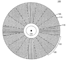
図1は、本発明のワイヤグリッド偏光器の実施例を一般的に100により示す。この実施例では、ワイヤグリッド偏光器上のエレメントパターンが接線方向に偏光された光を形成するように構成されている。図示のようにエレメント105は線形であり、複数の群(例えば2つの群120と125)にパターン化されている。ここで各群は複数のエレメントからなり、群は光軸(OA)を中心にする円形パターンに配置されている。破線115はエレメント間の分割線を示す。この実施例では、一方の群のエレメントは隣接する他方の群のエレメントに対して平行ではない。例えば群120は群125に隣接し、群120内のエレメントは相互に平行であり、群125のエレメントに対しては平行でない。
FIG. 1 shows an embodiment of a wire grid polarizer of the present invention, generally indicated at 100. In this embodiment, the element pattern on the wire grid polarizer is configured to form tangentially polarized light. As shown,
図1の偏光器では、延長された複数の導電性エレメント105が透明基板110により支持されている。エレメントの寸法とエレメント配置の寸法は使用される波長により決められ、紫外線光の全スペクトルに対して、または広いスペクトルに対して適合されている。所定の群ではエレメントはすべてが同じ長さではなく、群のエッジに向かって比較的に短くなる。このようにして、各群120、125は適切な「エッジ」形状を有し、これらの群を、光軸OAを中心にして放射状に円形パターンで配置することができる。
In the polarizer of FIG. 1, a plurality of extended
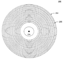
図2は、本発明のワイヤグリッド偏光器の別の実施例を一般的に200により示す。この実施例では、ワイヤグリッド偏光器上のエレメント250のパターンが、半径方向に偏光された光を形成するように構成されている。図示のように、複数のエレメント250が基板255上に同心円でパターン化されている。ここでもエレメントの寸法、およびエレメント配置の寸法は使用される波長により決められ、紫外線の全スペクトルに対して、または広いスペクトルに対して最適化されている。
FIG. 2 shows another embodiment of a wire grid polarizer of the present invention, generally designated 200. In this embodiment, the pattern of
グリッドエレメントと基板
本発明の実施例では、エレメントが基板上にパターン化されており、導電材料、例えば金属から形成される。エレメントは例えばアルミニウム、銀または金から形成することができる。このようなエレメントは制限されるものではないが、ワイヤまたはマイクロワイヤを含む。
Grid Element and Substrate In an embodiment of the present invention, the element is patterned on a substrate and is formed from a conductive material, such as a metal. The element can be formed from, for example, aluminum, silver or gold. Such elements include but are not limited to wires or microwires.
本発明の別の実施例では、偏光器の基板が紫外線光に対してすべて透過性であるかまたは部分的に透過性である。また制限されるものではないが基板は石英ガラス、フッ化カルシウム、サファイヤ、水晶およびフッ化マグネシウムのいずれかから形成される。本発明はこれに限定されるものではなく、他の厚さおよび材料を当業者であれば明白なように使用することができる。 In another embodiment of the present invention, the substrate of the polarizer is fully transmissive or partially transmissive to ultraviolet light. Although not limited, the substrate is formed of any one of quartz glass, calcium fluoride, sapphire, crystal, and magnesium fluoride. The present invention is not limited to this, and other thicknesses and materials can be used as will be apparent to those skilled in the art.
エレメント間の間隔は使用される波長により決められる。エレメント間の間隔は同心円パターンのエレメントに対してピッチと称される。このピッチは2つの隣接するエレメント上の対応するポイント間の間隔である。 The spacing between elements is determined by the wavelength used. The spacing between elements is referred to as the pitch for concentric pattern elements. This pitch is the spacing between corresponding points on two adjacent elements.
本発明の実施例では、エレメントの間隔は光の波長よりも小さい。従ってピッチは平行エレメントまたは同心円エレメントに対して近似的に200nmより小さくすることができ、平行エレメントに対しては隣接する平行でない2つのエレメント間の最も広いポイントにおいて200nmより小さい。実施例ではエレメントは、紫外線光の波長の1/10と波長の2倍の間の間隔で配置されている。 In an embodiment of the present invention, the element spacing is smaller than the wavelength of light. Thus, the pitch can be approximately less than 200 nm for parallel or concentric elements and is less than 200 nm for the parallel element at the widest point between two adjacent non-parallel elements. In the embodiment, the elements are arranged at an interval between 1/10 of the wavelength of ultraviolet light and twice the wavelength.
エレメント間の間隔は光の波長よりも小さくすることができるが、本発明はこれに制限されるものではない。エレメント間の間隔、およびとりわけ平行なエレメントのゾーン間の境界は光の波長より大きくすることもできる。 The distance between elements can be made smaller than the wavelength of light, but the present invention is not limited to this. The spacing between elements, and especially the boundaries between zones of parallel elements, can also be greater than the wavelength of light.
実施例では、本発明の偏光器のエレメントが紫外線波長の約1/4の周期、または約45nmから95nmの間の周期を有する。しかしこれに制限されるものではなく、他の周期と波長を使用することもできる。 In an embodiment, the polarizer element of the present invention has a period of about 1/4 of the ultraviolet wavelength, or a period between about 45 nm and 95 nm. However, the present invention is not limited to this, and other periods and wavelengths can be used.
実施例ではピッチは近似的に光波長の1/10または100nmである。比較的に長い周期(近似的に光波長の2倍より大きい)を備えるグリッドは回折格子として動作する。比較的に短い周期(近似的に光波長の1/2)のグリッドは偏光器として動作する。そして前記2つの周期の間の領域の周期のグリッドは回折格子として動作し、共振を基準にしての突然の変化または異常性を特徴とする。さらに偏光器のエレメントは規則的または等しい間隔を有する。択一的に本発明はこれに限定されるものではなく、不規則な間隔を有することもできる。 In the embodiment, the pitch is approximately 1/10 or 100 nm of the light wavelength. A grid with a relatively long period (approximately greater than twice the wavelength of the light) acts as a diffraction grating. A grid with a relatively short period (approximately 1/2 of the light wavelength) operates as a polarizer. The period grid in the region between the two periods operates as a diffraction grating and is characterized by a sudden change or anomaly with respect to resonance. Furthermore, the elements of the polarizer have regular or equal spacing. Alternatively, the present invention is not limited to this, and may have irregular intervals.
エレメントが線形である本発明の実施例では、エレメントは比較的長くて薄い。例えば各エレメントは一般的に紫外線波長よりも長い長さを有することができる。実施例ではこのエレメントは近似的に400nmから60nmの間の長さを有するが、これより長くても良い。 In embodiments of the invention where the element is linear, the element is relatively long and thin. For example, each element can generally have a length longer than the ultraviolet wavelength. In an embodiment, this element has a length approximately between 400 nm and 60 nm, but may be longer.
付加的に各エレメントはピッチの10%から90%の幅を有する。従ってこのエレメントは約10nmより大きな厚さを有し、約200nmよりは薄い。有利にはこのエレメントは近似的に20nmから100nmの間の厚さを有する。 In addition, each element has a width of 10% to 90% of the pitch. The element therefore has a thickness greater than about 10 nm and less than about 200 nm. The element preferably has a thickness of approximately between 20 nm and 100 nm.
エレメント幅は偏光器デバイスの性能を所定の適用に対して最適化するように選択することができる。一般的にピッチを基準にしてエレメント幅を増大すると、平行偏光に対する反射性をほぼ100%まで増大させることができる。一方、直交偏光に対する反射性も0%である理想値から増大してしまう。従って典型的には間隔に対するエレメント幅の比を大きくすると、透過光に対して高い吸光比が生じる。なぜなら平行偏光が透過しないからである。しかし直交偏光の一部が反射されるため高い効率は必要としない。逆に言えば一般的にピッチに対するエレメント幅の比が小さければ、反射されるビームに対して高い吸光比が生じるが、その際に高効率は必要ない。平行ビームに対する反射率と直交ビームに対する透過率の積として定義される全体効率は、エレメント幅のエレメントピッチに対する比が40%から60%であるときに最高となる。 The element width can be selected to optimize the performance of the polarizer device for a given application. In general, when the element width is increased with reference to the pitch, the reflectivity with respect to parallel polarized light can be increased to almost 100%. On the other hand, the reflectivity for orthogonally polarized light also increases from the ideal value of 0%. Thus, typically, increasing the ratio of element width to spacing results in a high extinction ratio for transmitted light. This is because parallel polarized light is not transmitted. However, high efficiency is not required because part of the orthogonal polarization is reflected. Conversely, generally speaking, if the ratio of the element width to the pitch is small, a high extinction ratio is generated for the reflected beam, but high efficiency is not required at that time. The overall efficiency, defined as the product of reflectivity for parallel beams and transmittance for orthogonal beams, is highest when the ratio of element width to element pitch is 40% to 60%.
装置
本発明はさらに本発明の偏光器を使用する装置を提供する。例えば本発明の偏光器は紫外線光を偏光するための装置に使用することができる。このような装置は例えば紫外線スペクトル中に少なくとも1つの波長を有する光ビームを形成する光源を有し、さらに基板を有し、この基板は紫外線スペクトルにある光に対して透明であり、光ビーム路に配置されており、さらに基板上にリソグラフでエッチングされたエレメントアレイを有する。ここで基板上にリソグラフでエッチングされたエレメントアレイは偏光された出射光を形成する。
Apparatus The present invention further provides an apparatus using the polarizer of the present invention. For example, the polarizer of the present invention can be used in an apparatus for polarizing ultraviolet light. Such an apparatus has, for example, a light source that forms a light beam having at least one wavelength in the ultraviolet spectrum, and further includes a substrate, the substrate being transparent to light in the ultraviolet spectrum, and a light beam path. And an element array etched lithographically on the substrate. Here, the element array etched lithographically on the substrate forms polarized outgoing light.
実施例では光源から放射された紫外線光は少なくとも2つの偏光方向を有し、ワイヤグリッド偏光器は第1偏光方向の光の大部分を反射し、第2偏光方向の光の大部分を透過する。 In an embodiment, the ultraviolet light emitted from the light source has at least two polarization directions, and the wire grid polarizer reflects most of the light in the first polarization direction and transmits most of the light in the second polarization direction. .
本発明はまた、ワイヤグリッド偏光器と照明器を有しており、光軸に沿った露光ビームを供給するための装置を提供する。ここで偏光器は紫外線光に対して透明な基板と、基板上にパターン化されたエレメントアレイとを有し、エレメントは紫外線光を偏光し、偏光器は照明器の瞳に偏光パターンを形成する。 The present invention also provides an apparatus for providing an exposure beam along an optical axis having a wire grid polarizer and an illuminator. Here, the polarizer has a substrate transparent to ultraviolet light and an element array patterned on the substrate, the element polarizes ultraviolet light, and the polarizer forms a polarization pattern on the pupil of the illuminator. .
本発明はさらに、光軸に沿って露光ビームを供給するための装置を提供するものであり、この装置はワイヤグリッド偏光器と投影光学系を有する。ここで偏光器は紫外線光に対して透明な基板と、基板上にパターン化されたエレメントのアレイを有し、エレメントは紫外線光を偏光し、偏光器は投影光学系に偏光パターンを形成する。 The invention further provides an apparatus for supplying an exposure beam along the optical axis, the apparatus comprising a wire grid polarizer and projection optics. Here, the polarizer has a substrate transparent to ultraviolet light and an array of elements patterned on the substrate, the elements polarize the ultraviolet light, and the polarizer forms a polarization pattern in the projection optical system.
本発明のワイヤグリッド偏光器はとりわけリソグラフの分野で有利であり、偏光された光を使用して、ウェハに比較的大きなコントラストを形成することができ、結果としてイメージングが改善される。一般的に偏光はリソグラフに4つの作用を及ぼす。(1)レチクルフィーチャの透過と回折、(2)投影光学系レンズでのフレネル損失、(3)レジスト表面でのフレンネル反射、そして(4)ベクトル干渉である。これら4つの要因を考慮すれば、リソグラフに対する偏光の理想的パターンを所定のレチクルおよび照明条件に対して変化することができる。 The wire grid polarizer of the present invention is particularly advantageous in the lithographic field, where polarized light can be used to create a relatively large contrast on the wafer, resulting in improved imaging. In general, polarization has four effects on the lithograph. (1) transmission and diffraction of reticle features, (2) Fresnel loss at the projection optics lens, (3) Frennel reflection at the resist surface, and (4) vector interference. Considering these four factors, the ideal pattern of polarization for a lithograph can be changed for a given reticle and illumination conditions.
リソグラフに対する理想的偏光パターンを変化することができるが、接線方向の偏光がしばしば満足できる選択肢である。レチクルは反復構造を有し、通常は水平方向または垂直方向にマスクと交差する。この構造はまた別の配向でも同様にレチクル上で反復される。構造を反復することは、1次元の回折格子のように行うことができ、光を1つの行で少数の密なビームに回折する。これらのビームが共にウェハに戻された場合、良好に干渉するなら、良好なイメージが得られる。非常に小さなフューチャをイメージングするのがもっとも困難である。非常に小さなフューチャの構造を反復すると、2つの回折配列が投影光学系瞳の対向エッジに形成される。多くの場合、接線方向の偏光がこのようなフューチャのイメージングに有利である。 While the ideal polarization pattern for a lithograph can be varied, tangential polarization is often a satisfactory option. The reticle has a repeating structure and usually intersects the mask in the horizontal or vertical direction. This structure is repeated on the reticle in different orientations as well. Repeating the structure can be done like a one-dimensional diffraction grating, diffracting light into a small number of dense beams in one row. If both of these beams are returned to the wafer, a good image is obtained if they interfere well. It is most difficult to image very small features. When repeating a very small feature structure, two diffractive arrays are formed at opposite edges of the projection optics pupil. In many cases, tangential polarization is advantageous for imaging such features.
同様に半径方向の偏光も所定の状況では有利である。例えば半径方向の偏光を使用することによりフレンネル損失を最小にすることができ、このことは光強度をさらに大きくする。従って半径方向の偏光が有利であるのは、高い光強度が所望される場合である。別の実施例では半径方向の偏光は、既に良好なコントラストを有するフューチャをイメージングするのに有利である。一方、コントラストの制限されたフューチャ(通常は非常に小さなフューチャ)をイメージングする場合には接線方向の偏光が所望されることとなる。 Similarly, radial polarization is also advantageous in certain situations. For example, the use of radial polarization can minimize the Frennel loss, which further increases the light intensity. Thus, radial polarization is advantageous when high light intensity is desired. In another embodiment, radial polarization is advantageous for imaging features that already have good contrast. On the other hand, when imaging features with limited contrast (usually very small features), tangential polarization is desired.
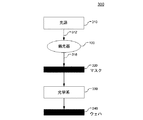
従って本発明は、半導体ウェハ上の感光性材料の層を露光するための光学的リソグラフシステム300を提供するものであり、このリソグラフシステムは本発明の偏光器を含む。図3に示すように、このようなシステム300は有利には放射エネルギー源としての光源310、本発明のワイヤグリッド偏光器100、マスク320,レンズ系のような投影光学系330,そして感光性材料の層340を含むウェハを有する。実施例では光源からの放射エネルギーは偏光器100を通過し、偏光器は光を所定の方向に偏光し、偏光された放射エネルギービーム318をマスク320に出力する。偏光された放射エネルギービーム318はマスク320を通過し、層3340を所定のパターンで露光する。
Accordingly, the present invention provides an optical
リソグラフではしばしば瞳全体が使用されないことを述べておく。従って瞳の所定の領域だけが所定のリソグラフ適用では照明される。例えば「ダイポール」照明では瞳のエッジで2つの領域だけが照明される。従ってリソグラフシステムの所定の実施例では、偏光器から出射するビームのすべてが使用されるわけではない。例えば偏光のパターンは瞳全体にわたって均一ではなく、または不完全である。このような場合、所望の偏光を有する瞳の一部だけが使用される。 Note that lithographs often do not use the entire pupil. Thus, only a predetermined area of the pupil is illuminated in a given lithographic application. For example, in “dipole” illumination, only two areas are illuminated at the edge of the pupil. Thus, in certain embodiments of a lithographic system, not all of the beam exiting the polarizer is used. For example, the pattern of polarization is not uniform throughout the pupil or is incomplete. In such a case, only a part of the pupil having the desired polarization is used.
本発明の別の実施例では、ワイヤグリッド偏光器100,200が有することのできる円弧が非常に広い角度を許容する。これにより偏光パターンを、光学システムのいずれの瞳面にも導入することができる。グリッドエレメントは偏光器として動作するから、さらなる簡素化のために非偏光ビームを上流側で使用することができる。いずれの偏光パターンも、ワイヤグリッドエレメントのパターンを選択することにより簡単に達成される。
In another embodiment of the invention, the arc that the
方法
導電性エレメントのアレイを基板上に配置することは、複数の周知技術により実行することができる。例えば米国特許第4049944号および米国特許第4514479号には、ホログラム干渉リソグラフを使用して、微細な格子構造をフォトレジストに形成し、続いてイオンビームによりエッチングしてこの構造体を基礎となる金属フィルムに変換することが記載されている。Stenkampは(“Grid polarizer for the visible spectral region”, Proceedings of the SPIE, vol.2213, pp.288-296)、ダイレクトe-beamリソグラフを使用してレジストパターンを形成し、続いてリアクティブイオンエッチングによりパターンを金属フィルムに変換することを開示している。極紫外線リソグラフおよびX線リソグラフ、X線ホログラム干渉リソグラフを含む他の高解像度リソグラス技術もレジストパターンを形成するに使用することができる。他のエッチングメカニズムおよびリフトオフプロセスを含む他の技術もパターンをレジストから金属フィルムに変換するのに使用することができる。導電性エレメントのアレイを形成するために使用される正確なプロセスは本発明に対しては重要でない。
Method Placing an array of conductive elements on a substrate can be performed by a number of well-known techniques. For example, US Pat. No. 4,049,944 and US Pat. No. 4,514,479 use a holographic interference lithograph to form a fine grating structure in a photoresist, followed by etching with an ion beam to form the underlying metal. Conversion to film is described. Stenkamp (“Grid polarizer for the visible spectral region”, Proceedings of the SPIE, vol. 2213, pp. 288-296) forms resist patterns using direct e-beam lithography, followed by reactive ion etching. To convert the pattern into a metal film. Other high resolution lithoglass techniques, including extreme ultraviolet lithographs, X-ray lithographs, and X-ray hologram interference lithographs, can also be used to form resist patterns. Other techniques including other etching mechanisms and lift-off processes can also be used to convert the pattern from resist to metal film. The exact process used to form the array of conductive elements is not critical to the present invention.
Claims (27)
(a)紫外線(UV)光に対して透明な基板と、
(b)該基板上にパターン化されたエレメントのアレイを有し、
該エレメントは紫外線光を偏光する、ことを特徴とする偏光器。 In patterned grid polarizers for use in lithographs,
(A) a substrate transparent to ultraviolet (UV) light;
(B) having an array of elements patterned on the substrate;
A polarizer characterized in that the element polarizes ultraviolet light.
該入射光は偏光器に入射し、出射光を偏光器から出射する。 The polarizer of claim 1, wherein the patterned element forms tangentially polarized outgoing light from unpolarized incident light;
The incident light enters the polarizer and the emitted light exits from the polarizer.
該入射光は偏光器に入射し、出射光を偏光器から出射する。 The polarizer of claim 1, wherein the patterned element forms radially polarized outgoing light from unpolarized incident light;
The incident light enters the polarizer and the emitted light exits from the polarizer.
該群は円形パターンに配置されており、
各群は平行なエレメントからなり、
第1の群のエレメントは第2の群のエレメントに対して平行ではない。 The polarizer of claim 1, wherein the elements are patterned into a plurality of groups.
The groups are arranged in a circular pattern;
Each group consists of parallel elements,
The first group of elements is not parallel to the second group of elements.
ワイヤグリッド偏光器は第1の偏光方向の光の大部分を反射し、第2の偏光方向の光の大部分を透過する。 The polarizer of claim 12, wherein the ultraviolet light has at least two polarization directions,
The wire grid polarizer reflects most of the light in the first polarization direction and transmits most of the light in the second polarization direction.
(a)紫外線スペクトル中に少なくとも1つの波長を有する光ビームを形成する光源と、
(b)紫外線スペクトルの光に対して透明であり、光ビームの経路に配置された基板と、
(c)基板上にあるエレメントのアレイと、
を有する装置において、
エレメントのアレイは入射紫外線光を偏光し、偏光された光を出射する、ことを特徴とする装置。 An apparatus for polarizing ultraviolet light,
(A) a light source that forms a light beam having at least one wavelength in the ultraviolet spectrum;
(B) a substrate that is transparent to light in the ultraviolet spectrum and disposed in the path of the light beam;
(C) an array of elements on a substrate;
In a device having
The device is characterized in that the array of elements polarizes incident ultraviolet light and emits polarized light.
(a)ワイヤグリッド偏光器と、
(b)瞳を備える照明器と、
を有する形式の装置において、
偏光器は、紫外線(UV)光に対して透明な基板と、基板上にパターン化されたエレメントのアレイを有し、該エレメントは紫外線光を偏光し、偏光パターンを紫外線光中に照明器の瞳で形成する、ことを特徴とする装置。 An apparatus for forming an exposure beam along an optical path,
(A) a wire grid polarizer;
(B) an illuminator comprising a pupil;
In a device of the type having
The polarizer has a substrate that is transparent to ultraviolet (UV) light and an array of elements patterned on the substrate, the element polarizes the ultraviolet light and the polarization pattern into the ultraviolet light. A device characterized by being formed with a pupil.
(a)ワイヤグリッド偏光器と、
(b)投影光学系と、
を有する形式の装置において、
偏光器は、紫外線(UV)光に対して透明な基板と、基板上にパターン化されたエレメントのアレイを有し、該エレメントは紫外線光を偏光し、偏光パターンを投影光学系に向かう紫外線光出力中に形成する、ことを特徴とする装置。 An apparatus for forming an exposure beam along an optical path,
(A) a wire grid polarizer;
(B) a projection optical system;
In a device of the type having
The polarizer has a substrate that is transparent to ultraviolet (UV) light and an array of elements patterned on the substrate, the elements polarizing the ultraviolet light and directing the polarization pattern to the projection optics. A device characterized by forming during output.
Applications Claiming Priority (1)
| Application Number | Priority Date | Filing Date | Title |
|---|---|---|---|
| US10/813,168 US7304719B2 (en) | 2004-03-31 | 2004-03-31 | Patterned grid element polarizer |
Publications (2)
| Publication Number | Publication Date |
|---|---|
| JP2005292835A true JP2005292835A (en) | 2005-10-20 |
| JP4264071B2 JP4264071B2 (en) | 2009-05-13 |
Family
ID=34887695
Family Applications (1)
| Application Number | Title | Priority Date | Filing Date |
|---|---|---|---|
| JP2005103166A Expired - Fee Related JP4264071B2 (en) | 2004-03-31 | 2005-03-31 | Lithographic apparatus |
Country Status (7)
| Country | Link |
|---|---|
| US (1) | US7304719B2 (en) |
| EP (1) | EP1582894B1 (en) |
| JP (1) | JP4264071B2 (en) |
| KR (1) | KR100664623B1 (en) |
| CN (1) | CN100388026C (en) |
| SG (1) | SG115821A1 (en) |
| TW (1) | TWI305279B (en) |
Cited By (5)
| Publication number | Priority date | Publication date | Assignee | Title |
|---|---|---|---|---|
| JP2007128086A (en) * | 2005-10-31 | 2007-05-24 | Toshiba Corp | Short wavelength polarizing element and polarizing element manufacturing method |
| JP2007128087A (en) * | 2005-10-31 | 2007-05-24 | Toshiba Corp | Short wavelength polarizing element and polarizing element manufacturing method |
| JP2010134411A (en) * | 2008-11-07 | 2010-06-17 | Ricoh Co Ltd | Polarization splitting device, method of manufacturing polarization beam splitter, optical scanning device, and image forming apparatus |
| KR20110133571A (en) * | 2009-03-03 | 2011-12-13 | 인터내셔널 비지네스 머신즈 코포레이션 | Optical lithography apparatus |
| WO2025164595A1 (en) * | 2024-01-29 | 2025-08-07 | 株式会社フォトニックラティス | Polarization mask for photo-alignment exposure, photo-alignment exposure method, and method for manufacturing optical component or the like |
Families Citing this family (58)
| Publication number | Priority date | Publication date | Assignee | Title |
|---|---|---|---|---|
| US20070019179A1 (en) | 2004-01-16 | 2007-01-25 | Damian Fiolka | Polarization-modulating optical element |
| US8270077B2 (en) | 2004-01-16 | 2012-09-18 | Carl Zeiss Smt Gmbh | Polarization-modulating optical element |
| CN101799587B (en) | 2004-01-16 | 2012-05-30 | 卡尔蔡司Smt有限责任公司 | Optical system, projection system and manufacturing method of micro-structure semiconductor component |
| JP4451268B2 (en) * | 2004-03-04 | 2010-04-14 | 株式会社リコー | Optical element and manufacturing method thereof, optical product using the same, optical pickup, and optical information processing apparatus |
| US7304719B2 (en) | 2004-03-31 | 2007-12-04 | Asml Holding N.V. | Patterned grid element polarizer |
| US7324280B2 (en) | 2004-05-25 | 2008-01-29 | Asml Holding N.V. | Apparatus for providing a pattern of polarization |
| US7548370B2 (en) * | 2004-06-29 | 2009-06-16 | Asml Holding N.V. | Layered structure for a tile wave plate assembly |
| DE102004040534B4 (en) * | 2004-08-20 | 2006-06-14 | Carl Zeiss Jena Gmbh | Diffractive polarization-separating element for unpolarized electromagnetic radiation in the UV range, system with two such elements and method for producing such an element |
| JP4479535B2 (en) * | 2005-02-21 | 2010-06-09 | セイコーエプソン株式会社 | Optical element manufacturing method |
| DE102006032810A1 (en) | 2006-07-14 | 2008-01-17 | Carl Zeiss Smt Ag | Illumination optics for a microlithography projection exposure apparatus, illumination system with such an illumination optics, microlithography projection exposure apparatus with such an illumination system, microlithographic production method for components and component produced by this method |
| TWI307677B (en) * | 2006-07-18 | 2009-03-21 | Applied Res Lab | Method and device for fabricating nano-structure with patterned particle beam |
| US8792161B2 (en) * | 2007-02-21 | 2014-07-29 | Globalfoundries Inc. | Optical polarizer with nanotube array |
| US7777943B2 (en) * | 2007-03-01 | 2010-08-17 | American Museum Of Natural History | Astrometry and photometry with coronagraphs |
| US8643822B2 (en) * | 2007-07-03 | 2014-02-04 | Jds Uniphase Corporation | Non-etched flat polarization-selective diffractive optical elements |
| DE102008002749A1 (en) * | 2008-06-27 | 2009-12-31 | Carl Zeiss Smt Ag | Illumination optics for microlithography |
| JP2011013654A (en) * | 2008-10-23 | 2011-01-20 | Seiko Epson Corp | Multilayer antireflection layer and method of producing the same, and plastic lens |
| JP2010197352A (en) * | 2009-02-27 | 2010-09-09 | Hitachi High-Technologies Corp | Defect inspection method and defect inspecting apparatus |
| JP2010231171A (en) * | 2009-03-04 | 2010-10-14 | Seiko Epson Corp | Optical article and manufacturing method thereof |
| JP2010231172A (en) * | 2009-03-04 | 2010-10-14 | Seiko Epson Corp | Optical article and manufacturing method thereof |
| JP2011053660A (en) * | 2009-08-05 | 2011-03-17 | Hoya Corp | Polarizing lens |
| JP5588135B2 (en) * | 2009-08-10 | 2014-09-10 | ホーヤ レンズ マニュファクチャリング フィリピン インク | Method for manufacturing optical article |
| JP5523066B2 (en) * | 2009-11-17 | 2014-06-18 | ホーヤ レンズ マニュファクチャリング フィリピン インク | Method for manufacturing optical article |
| US10274650B2 (en) | 2010-01-29 | 2019-04-30 | Beam Engineering For Advanced Measurements Co. | Diffractive waveplate lenses and applications |
| US11366254B2 (en) | 2010-01-29 | 2022-06-21 | Beam Engineering For Advanced Measurements Co. | High-efficiency wide-angle beam steering system |
| US9557456B2 (en) | 2010-01-29 | 2017-01-31 | The United States Of America As Represented By The Secretary Of The Army | Broadband optics for manipulating light beams and images |
| US10114239B2 (en) | 2010-04-21 | 2018-10-30 | Beam Engineering For Advanced Measurements Co. | Waveplate lenses and methods for their fabrication |
| US9983479B2 (en) * | 2010-04-21 | 2018-05-29 | Beam Engineering For Advanced Measurements Co. | Fabrication of high efficiency, high quality, large area diffractive waveplates and arrays |
| US10197715B1 (en) | 2013-03-15 | 2019-02-05 | Beam Engineering For Advanced Measurements Co. | Methods of diffractive lens and mirror fabrication |
| US20110262844A1 (en) | 2010-04-21 | 2011-10-27 | Beam Engineering For Advanced Measurement Co. | Fabrication of high efficiency, high quality, large area diffractive waveplates and arrays |
| US8625107B2 (en) * | 2010-05-19 | 2014-01-07 | Uwm Research Foundation, Inc. | Target for motion tracking system |
| CN101938080B (en) * | 2010-06-25 | 2011-11-30 | 北京交通大学 | An active optical fiber with single-mode output TM01 mode characteristics |
| JP2012032690A (en) | 2010-08-02 | 2012-02-16 | Seiko Epson Corp | Optical article and manufacturing method thereof |
| CN102722034B (en) * | 2012-02-11 | 2015-10-07 | 深圳市光峰光电技术有限公司 | Light splitting device and relevant source |
| DE102012205554A1 (en) * | 2012-04-04 | 2013-04-25 | Carl Zeiss Smt Gmbh | Optical system for microlithography system used for production of microstructured components, has beam deflecting device with beam deflecting element, which focuses incident light in plane of wafer |
| DE102012206151A1 (en) * | 2012-04-16 | 2013-05-02 | Carl Zeiss Smt Gmbh | Optical system for microlithographic projection exposure system utilized for manufacturing e.g. LCD, has screen polarizer converting linear polarization distribution with polarization direction of bundle into mixed polarization distribution |
| DE102013202590A1 (en) * | 2013-02-19 | 2014-09-04 | Carl Zeiss Smt Gmbh | EUV light source for generating a useful output beam for a projection exposure apparatus |
| US10107945B2 (en) | 2013-03-01 | 2018-10-23 | Beam Engineering For Advanced Measurements Co. | Vector vortex waveplates |
| US10185182B2 (en) * | 2013-03-03 | 2019-01-22 | Beam Engineering For Advanced Measurements Co. | Mechanical rubbing method for fabricating cycloidal diffractive waveplates |
| DE102013207502A1 (en) | 2013-04-25 | 2014-05-15 | Carl Zeiss Smt Gmbh | Optical system for wafer and mask inspection plant, has polarizing elements which are designed such that polarization distribution set to micro-structured element is not changed by changing operating wavelength |
| DE102013209042A1 (en) | 2013-05-15 | 2014-05-08 | Carl Zeiss Smt Gmbh | Optical system for use in micro lithographic projection exposure system, has periodic grating structures made from material, where intensity of electromagnetic radiation in beam path amounts to maximum percentages of intensity of radiation |
| CA2941274C (en) | 2014-03-04 | 2020-02-25 | Novadaq Technologies Inc. | Spatial and spectral filtering apertures and optical imaging systems including the same |
| CN106605164B (en) | 2014-03-04 | 2020-04-24 | 诺瓦达克技术公司 | Relay lens system for broadband imaging |
| KR102413901B1 (en) * | 2015-04-24 | 2022-06-28 | 삼성디스플레이 주식회사 | Wire grid polarizer plate and display device including the same |
| US9976911B1 (en) | 2015-06-30 | 2018-05-22 | Beam Engineering For Advanced Measurements Co. | Full characterization wavefront sensor |
| US10191296B1 (en) | 2015-06-30 | 2019-01-29 | Beam Engineering For Advanced Measurements Co. | Laser pointer with reduced risk of eye injury |
| KR102427155B1 (en) * | 2015-08-25 | 2022-07-29 | 삼성디스플레이 주식회사 | Laser crystalling apparatus |
| CN108431649B (en) | 2015-08-31 | 2021-08-24 | 史赛克欧洲运营有限公司 | Polarization-dependent filters, systems using the same, and associated toolkits and methods |
| US10436957B2 (en) | 2015-10-27 | 2019-10-08 | Beam Engineering For Advanced Measurements Co. | Broadband imaging with diffractive waveplate coated mirrors and diffractive waveplate objective lens |
| WO2017151291A1 (en) * | 2016-03-04 | 2017-09-08 | Applied Materials, Inc. | Wire grid polarizer manufacturing method |
| EP3270237B1 (en) * | 2016-07-13 | 2018-11-07 | The Swatch Group Research and Development Ltd. | Portable object including a device for displaying at least one item of information viewed through a wave plate |
| US10423045B2 (en) | 2016-11-14 | 2019-09-24 | Beam Engineering For Advanced Measurements Co. | Electro-optical diffractive waveplate beam shaping system |
| KR101852071B1 (en) * | 2016-12-28 | 2018-04-26 | 한국과학기술연구원 | Metamaterial for electromagnetic wave filter |
| US10274805B2 (en) | 2017-06-13 | 2019-04-30 | Beam Engineering For Advanced Measurements Co. | Polarization-independent switchable lens system |
| US11175441B1 (en) | 2018-03-05 | 2021-11-16 | Beam Engineering For Advanced Measurements Co. | Polarization-independent diffractive optical structures |
| US11982906B1 (en) | 2018-03-05 | 2024-05-14 | Beam Engineering For Advanced Measurements Co. | Polarization-independent diffractive optical structures |
| CN109254341A (en) * | 2018-10-31 | 2019-01-22 | 南京奥谱依电子科技有限公司 | A patterned polarized film and its preparation method |
| CN111239878A (en) * | 2018-11-09 | 2020-06-05 | 英属开曼群岛商音飞光电科技股份有限公司 | Grating plate device |
| US11294240B2 (en) | 2019-08-10 | 2022-04-05 | Beam Engineering For Advanced Measurements Co. | Diffractive waveplate devices that operate over a wide temperature range |
Family Cites Families (32)
| Publication number | Priority date | Publication date | Assignee | Title |
|---|---|---|---|---|
| US3719415A (en) * | 1971-09-22 | 1973-03-06 | Bell Telephone Labor Inc | Radial and tangential polarizers |
| US3877789A (en) * | 1972-11-08 | 1975-04-15 | Marie G R P | Mode transformer for light or millimeter electromagnetic waves |
| US4049944A (en) | 1973-02-28 | 1977-09-20 | Hughes Aircraft Company | Process for fabricating small geometry semiconductive devices including integrated components |
| US4514479A (en) | 1980-07-01 | 1985-04-30 | The United States Of America As Represented By The Secretary Of The Navy | Method of making near infrared polarizers |
| JP2796005B2 (en) | 1992-02-10 | 1998-09-10 | 三菱電機株式会社 | Projection exposure apparatus and polarizer |
| JPH05307112A (en) * | 1992-04-28 | 1993-11-19 | Satoyuki Saito | Polarizing plate |
| JPH08184711A (en) | 1994-12-29 | 1996-07-16 | Sony Corp | Polarizing optical element |
| DE19535392A1 (en) | 1995-09-23 | 1997-03-27 | Zeiss Carl Fa | Radial polarization-rotating optical arrangement and microlithography projection exposure system with it |
| KR0171947B1 (en) * | 1995-12-08 | 1999-03-20 | 김주용 | Exposure method for manufacturing semiconductor device and exposure device using same |
| DE19621512A1 (en) * | 1996-05-29 | 1997-12-04 | Univ Schiller Jena | Polarisation establishment with respect to wavelength of source spectra |
| EP1002221B1 (en) * | 1997-08-06 | 2003-07-02 | INSTITUT FÜR MIKROTECHNIK MAINZ GmbH | Micropolarimeter |
| EP1003078A3 (en) | 1998-11-17 | 2001-11-07 | Corning Incorporated | Replicating a nanoscale pattern |
| US6122103A (en) | 1999-06-22 | 2000-09-19 | Moxtech | Broadband wire grid polarizer for the visible spectrum |
| RU2166819C2 (en) | 1999-08-09 | 2001-05-10 | Низьев Владимир Григорьевич | Laser resonator optical element |
| AU7309400A (en) * | 1999-09-15 | 2001-04-17 | Yeda Research And Development Co. Ltd. | Optical resonators with orthogonally polarized modes |
| US20020167727A1 (en) | 2001-03-27 | 2002-11-14 | Hansen Douglas P. | Patterned wire grid polarizer and method of use |
| DE10124566A1 (en) | 2001-05-15 | 2002-11-21 | Zeiss Carl | Optical imaging system with polarizing agents and quartz crystal plate therefor |
| DE10124803A1 (en) * | 2001-05-22 | 2002-11-28 | Zeiss Carl | Polarizer and microlithography projection system with polarizer |
| US6784991B2 (en) * | 2001-06-18 | 2004-08-31 | Therma-Wave, Inc. | Diffractive optical elements and grid polarizers in focusing spectroscopic ellipsometers |
| US6813077B2 (en) | 2001-06-19 | 2004-11-02 | Corning Incorporated | Method for fabricating an integrated optical isolator and a novel wire grid structure |
| US20030206337A1 (en) | 2002-05-06 | 2003-11-06 | Eastman Kodak Company | Exposure apparatus for irradiating a sensitized substrate |
| US6785050B2 (en) | 2002-05-09 | 2004-08-31 | Moxtek, Inc. | Corrosion resistant wire-grid polarizer and method of fabrication |
| US6876784B2 (en) | 2002-05-30 | 2005-04-05 | Nanoopto Corporation | Optical polarization beam combiner/splitter |
| US6874899B2 (en) * | 2002-07-12 | 2005-04-05 | Eastman Kodak Company | Apparatus and method for irradiating a substrate |
| CN1281982C (en) | 2002-09-10 | 2006-10-25 | 清华大学 | Polarized element and method for manufacturing same |
| US7190521B2 (en) * | 2002-09-13 | 2007-03-13 | Technion Research And Development Foundation Ltd. | Space-variant subwavelength dielectric grating and applications thereof |
| US7090964B2 (en) * | 2003-02-21 | 2006-08-15 | Asml Holding N.V. | Lithographic printing with polarized light |
| US6943941B2 (en) * | 2003-02-27 | 2005-09-13 | Asml Netherlands B.V. | Stationary and dynamic radial transverse electric polarizer for high numerical aperture systems |
| US7206059B2 (en) | 2003-02-27 | 2007-04-17 | Asml Netherlands B.V. | Stationary and dynamic radial transverse electric polarizer for high numerical aperture systems |
| AU2003304304A1 (en) * | 2003-07-05 | 2005-01-21 | Carl Zeiss Smt Ag | Device for the polarization-specific examination of an optical system |
| US6970233B2 (en) * | 2003-12-03 | 2005-11-29 | Texas Instruments Incorporated | System and method for custom-polarized photolithography illumination |
| US7304719B2 (en) | 2004-03-31 | 2007-12-04 | Asml Holding N.V. | Patterned grid element polarizer |
-
2004
- 2004-03-31 US US10/813,168 patent/US7304719B2/en not_active Expired - Fee Related
-
2005
- 2005-03-28 TW TW094109628A patent/TWI305279B/en not_active IP Right Cessation
- 2005-03-30 SG SG200501994A patent/SG115821A1/en unknown
- 2005-03-30 KR KR1020050026421A patent/KR100664623B1/en not_active Expired - Fee Related
- 2005-03-30 EP EP05006957A patent/EP1582894B1/en not_active Expired - Lifetime
- 2005-03-31 CN CNB2005100600552A patent/CN100388026C/en not_active Expired - Fee Related
- 2005-03-31 JP JP2005103166A patent/JP4264071B2/en not_active Expired - Fee Related
Cited By (7)
| Publication number | Priority date | Publication date | Assignee | Title |
|---|---|---|---|---|
| JP2007128086A (en) * | 2005-10-31 | 2007-05-24 | Toshiba Corp | Short wavelength polarizing element and polarizing element manufacturing method |
| JP2007128087A (en) * | 2005-10-31 | 2007-05-24 | Toshiba Corp | Short wavelength polarizing element and polarizing element manufacturing method |
| US8687274B2 (en) | 2005-10-31 | 2014-04-01 | Kabushiki Kaisha Toshiba | Short-wavelength polarizing elements and the manufacture and use thereof |
| JP2010134411A (en) * | 2008-11-07 | 2010-06-17 | Ricoh Co Ltd | Polarization splitting device, method of manufacturing polarization beam splitter, optical scanning device, and image forming apparatus |
| KR20110133571A (en) * | 2009-03-03 | 2011-12-13 | 인터내셔널 비지네스 머신즈 코포레이션 | Optical lithography apparatus |
| KR101599097B1 (en) | 2009-03-03 | 2016-03-02 | 인터내셔널 비지네스 머신즈 코포레이션 | Optical lithography apparatus |
| WO2025164595A1 (en) * | 2024-01-29 | 2025-08-07 | 株式会社フォトニックラティス | Polarization mask for photo-alignment exposure, photo-alignment exposure method, and method for manufacturing optical component or the like |
Also Published As
| Publication number | Publication date |
|---|---|
| TWI305279B (en) | 2009-01-11 |
| KR100664623B1 (en) | 2007-01-04 |
| CN1677141A (en) | 2005-10-05 |
| EP1582894B1 (en) | 2011-10-05 |
| TW200532260A (en) | 2005-10-01 |
| KR20060045138A (en) | 2006-05-16 |
| US20050219696A1 (en) | 2005-10-06 |
| JP4264071B2 (en) | 2009-05-13 |
| CN100388026C (en) | 2008-05-14 |
| US7304719B2 (en) | 2007-12-04 |
| SG115821A1 (en) | 2005-10-28 |
| EP1582894A1 (en) | 2005-10-05 |
Similar Documents
| Publication | Publication Date | Title |
|---|---|---|
| JP4264071B2 (en) | Lithographic apparatus | |
| TWI280460B (en) | Apparatus for providing a pattern of polarization | |
| JP4832477B2 (en) | Lithographic projection apparatus and polarizer device | |
| KR101709376B1 (en) | A method and apparatus for printing a periodic pattern with large depth of focus | |
| US7548370B2 (en) | Layered structure for a tile wave plate assembly | |
| US9036133B2 (en) | Lithographic fabrication of general periodic structures by exposing a photosensitive layer to a range of lateral intensity distributions | |
| JP5173309B2 (en) | Hologram, exposure apparatus and device manufacturing method | |
| KR20010089153A (en) | Diffractive element in extreme-UV lithography condenser | |
| CN101634813A (en) | Apparatus for exposing a substrate, photomask and modified illuminating system of the apparatus, and method of forming a pattern on a substrate using the apparatus | |
| TWI293696B (en) | Optical system for spatially controlling ligth polarization and method for manufacturing the same | |
| US5717218A (en) | Focal plane phase-shifting lithography | |
| US7629087B2 (en) | Photomask, method of making a photomask and photolithography method and system using the same | |
| JP2009162939A (en) | Computer generated hologram and exposure apparatus | |
| US20050094271A1 (en) | Hybrid optical component for x ray applications and method associated therewith | |
| EP1451629A1 (en) | Homogenizer | |
| JP5078765B2 (en) | Computer generated hologram, exposure apparatus and device manufacturing method | |
| Vladimirsky et al. | Fabrication of free-standing x-ray transmission gratings and zone plates | |
| US20050123840A1 (en) | Mask for use in a microlithographic projection exposure apparatus | |
| JP2006284960A (en) | Diffraction grating, diffraction grating manufacturing method, exposure method using the diffraction grating, electronic device manufacturing method, electronic device, and exposure apparatus | |
| Zhang et al. | Model of freeform illumination mode and polarization mode for 193nm immersion lithographic machine |
Legal Events
| Date | Code | Title | Description |
|---|---|---|---|
| RD04 | Notification of resignation of power of attorney |
Free format text: JAPANESE INTERMEDIATE CODE: A7424 Effective date: 20060914 |
|
| A521 | Request for written amendment filed |
Free format text: JAPANESE INTERMEDIATE CODE: A821 Effective date: 20060915 |
|
| RD03 | Notification of appointment of power of attorney |
Free format text: JAPANESE INTERMEDIATE CODE: A7423 Effective date: 20060904 |
|
| A131 | Notification of reasons for refusal |
Free format text: JAPANESE INTERMEDIATE CODE: A131 Effective date: 20080115 |
|
| A521 | Request for written amendment filed |
Free format text: JAPANESE INTERMEDIATE CODE: A523 Effective date: 20080415 |
|
| A131 | Notification of reasons for refusal |
Free format text: JAPANESE INTERMEDIATE CODE: A131 Effective date: 20080918 |
|
| A521 | Request for written amendment filed |
Free format text: JAPANESE INTERMEDIATE CODE: A523 Effective date: 20081211 |
|
| TRDD | Decision of grant or rejection written | ||
| A01 | Written decision to grant a patent or to grant a registration (utility model) |
Free format text: JAPANESE INTERMEDIATE CODE: A01 Effective date: 20090115 |
|
| A01 | Written decision to grant a patent or to grant a registration (utility model) |
Free format text: JAPANESE INTERMEDIATE CODE: A01 |
|
| A61 | First payment of annual fees (during grant procedure) |
Free format text: JAPANESE INTERMEDIATE CODE: A61 Effective date: 20090213 |
|
| FPAY | Renewal fee payment (event date is renewal date of database) |
Free format text: PAYMENT UNTIL: 20120220 Year of fee payment: 3 |
|
| R150 | Certificate of patent or registration of utility model |
Free format text: JAPANESE INTERMEDIATE CODE: R150 |
|
| S802 | Written request for registration of partial abandonment of right |
Free format text: JAPANESE INTERMEDIATE CODE: R311802 |
|
| FPAY | Renewal fee payment (event date is renewal date of database) |
Free format text: PAYMENT UNTIL: 20120220 Year of fee payment: 3 |
|
| R350 | Written notification of registration of transfer |
Free format text: JAPANESE INTERMEDIATE CODE: R350 |
|
| FPAY | Renewal fee payment (event date is renewal date of database) |
Free format text: PAYMENT UNTIL: 20130220 Year of fee payment: 4 |
|
| FPAY | Renewal fee payment (event date is renewal date of database) |
Free format text: PAYMENT UNTIL: 20130220 Year of fee payment: 4 |
|
| FPAY | Renewal fee payment (event date is renewal date of database) |
Free format text: PAYMENT UNTIL: 20140220 Year of fee payment: 5 |
|
| R250 | Receipt of annual fees |
Free format text: JAPANESE INTERMEDIATE CODE: R250 |
|
| R250 | Receipt of annual fees |
Free format text: JAPANESE INTERMEDIATE CODE: R250 |
|
| R250 | Receipt of annual fees |
Free format text: JAPANESE INTERMEDIATE CODE: R250 |
|
| LAPS | Cancellation because of no payment of annual fees |