EP1002221B1 - Mikropolarimeter - Google Patents
Mikropolarimeter Download PDFInfo
- Publication number
- EP1002221B1 EP1002221B1 EP97938882A EP97938882A EP1002221B1 EP 1002221 B1 EP1002221 B1 EP 1002221B1 EP 97938882 A EP97938882 A EP 97938882A EP 97938882 A EP97938882 A EP 97938882A EP 1002221 B1 EP1002221 B1 EP 1002221B1
- Authority
- EP
- European Patent Office
- Prior art keywords
- micropolarimeter
- analyzer
- segments
- detector
- polarization
- Prior art date
- Legal status (The legal status is an assumption and is not a legal conclusion. Google has not performed a legal analysis and makes no representation as to the accuracy of the status listed.)
- Expired - Lifetime
Links
Images


Classifications
-
- G—PHYSICS
- G01—MEASURING; TESTING
- G01J—MEASUREMENT OF INTENSITY, VELOCITY, SPECTRAL CONTENT, POLARISATION, PHASE OR PULSE CHARACTERISTICS OF INFRARED, VISIBLE OR ULTRAVIOLET LIGHT; COLORIMETRY; RADIATION PYROMETRY
- G01J4/00—Measuring polarisation of light
- G01J4/04—Polarimeters using electric detection means
-
- Y—GENERAL TAGGING OF NEW TECHNOLOGICAL DEVELOPMENTS; GENERAL TAGGING OF CROSS-SECTIONAL TECHNOLOGIES SPANNING OVER SEVERAL SECTIONS OF THE IPC; TECHNICAL SUBJECTS COVERED BY FORMER USPC CROSS-REFERENCE ART COLLECTIONS [XRACs] AND DIGESTS
- Y10—TECHNICAL SUBJECTS COVERED BY FORMER USPC
- Y10S—TECHNICAL SUBJECTS COVERED BY FORMER USPC CROSS-REFERENCE ART COLLECTIONS [XRACs] AND DIGESTS
- Y10S977/00—Nanotechnology
- Y10S977/70—Nanostructure
- Y10S977/773—Nanoparticle, i.e. structure having three dimensions of 100 nm or less
-
- Y—GENERAL TAGGING OF NEW TECHNOLOGICAL DEVELOPMENTS; GENERAL TAGGING OF CROSS-SECTIONAL TECHNOLOGIES SPANNING OVER SEVERAL SECTIONS OF THE IPC; TECHNICAL SUBJECTS COVERED BY FORMER USPC CROSS-REFERENCE ART COLLECTIONS [XRACs] AND DIGESTS
- Y10—TECHNICAL SUBJECTS COVERED BY FORMER USPC
- Y10S—TECHNICAL SUBJECTS COVERED BY FORMER USPC CROSS-REFERENCE ART COLLECTIONS [XRACs] AND DIGESTS
- Y10S977/00—Nanotechnology
- Y10S977/70—Nanostructure
- Y10S977/832—Nanostructure having specified property, e.g. lattice-constant, thermal expansion coefficient
- Y10S977/834—Optical properties of nanomaterial, e.g. specified transparency, opacity, or index of refraction
-
- Y—GENERAL TAGGING OF NEW TECHNOLOGICAL DEVELOPMENTS; GENERAL TAGGING OF CROSS-SECTIONAL TECHNOLOGIES SPANNING OVER SEVERAL SECTIONS OF THE IPC; TECHNICAL SUBJECTS COVERED BY FORMER USPC CROSS-REFERENCE ART COLLECTIONS [XRACs] AND DIGESTS
- Y10—TECHNICAL SUBJECTS COVERED BY FORMER USPC
- Y10S—TECHNICAL SUBJECTS COVERED BY FORMER USPC CROSS-REFERENCE ART COLLECTIONS [XRACs] AND DIGESTS
- Y10S977/00—Nanotechnology
- Y10S977/902—Specified use of nanostructure
- Y10S977/932—Specified use of nanostructure for electronic or optoelectronic application
- Y10S977/953—Detector using nanostructure
- Y10S977/957—Of chemical property or presence
Definitions
- the invention relates to a micropolarimeter with an analyzer made of a polarization material, in which the polarization is based on absorption effects within the material, and with a detector arranged in the radiation direction behind the analyzer and having a number N D 3 3 of segments, the area of the analyzer being larger is equal to that of the segment areas of the detector.
- a disadvantage is the strict monochrome of this cone polarimeter, because the polarizing layer system is a narrow band filter that can only be used in the desired selectivity for a very narrow spectral range Has polarization. Spectral applications or switching to other than the design wavelength is therefore excluded.
- Another disadvantage is the technologically complex production of the polarizing layer system. So the coating has a very steep angle. In addition, a high degree of homogeneity Layer parameters required on the outer surface. These requirements can not with common coating systems for vertical Coating geometries are applied, are met.
- the reason for the relatively low degree of polarization in lattice polarizers is the selective reflection of the vibrating parallel to the grid lines Components of the electric field. Since this is one Surface effect. can only be a finite per unit area Degree of polarization can be achieved. So at a wavelength of 670 nm for a lattice with a lattice constant of 100 nm a theoretical achievable degree of polarization of approximately 100 determined. Such one Lattice made by electron lithography practically only delivers values from 2 to 3 (see B. Stenkamp et al. "Grid Polarizer for the Visible Spectral Region ". SPIE Proceedings Vol 2213).
- lattice polarizers The theoretically possible degree of polarization of lattice polarizers depends largely depends on the ratio of the lattice constants to the wavelength. For one optimal effect, the wavelength should be greater than the grating constant. In the visible spectral range, this means lattice constants below 100 nm, which is difficult to manufacture. So is the realization of this arrangement Use of electron beam lithography in connection with complex thin film technology Processes required. Both are very high Associated costs. Therefore, such lattice polarizers have been used mainly made for applications in infrared, where at wavelengths from a few 10 ⁇ m to 100 ⁇ m the conventional photolithography with a Resolution of approx. 1 ⁇ m can be used.
- DE 44 42 400 A1 discloses a sensor for determining the position in space, a cone breaking a beam and a cylindrical one Has transition element, which is arranged on a detector array.
- the Cone can be provided with an interference layer system around the beacon separate from parasitic radiation. The polarization of the beacon can with this arrangement cannot be measured.
- the object of the invention is to provide a micropolarimeter without moving parts create that has a high degree of polarization with improved adjustment, can be used for polychromatic light that is so small that the beam from common lasers can be detected in one measuring step without additional expansion can, and easily expanded to a complete Stokesmeter can be.
- the cut edges For the production of segments for a micropolarimeter are preferred microtechnical processes applied to the optical quality of the get used analyzer. It plays with the dimensions used the quality of the cut edges compared to macroscopic cuts a major role. Poor quality of the edges would scatter and thus depolarization, i.e. a decrease in the degree of polarization, cause. Therefore, the cut edges should only be smaller irregularities have than 10 ⁇ m.
- the nanometer-sized particles are Macroscopically aligned along the desired optical axis and in the organic or inorganic matrix. It is preferably is a polarization material that contains nanometer-sized particles with strong Contains anisotropy of optical conductivity. This is advantageous Polarization material glass with embedded silver particles.
- the analyzer disk can be in one piece, wherein the direction of polarization is radial or tangential.
- the segments can be sectors or even flat structures of other shapes, e.g. rectangular or oval segments, the segments also being spaced apart can be arranged to each other.
- each segment of the analyzer is triangular or trapezoidal blank of a polarization material is formed, in which the Polarization is based on absorption effects within the material.
- the segments of the analyzer disk do not necessarily have to have a radial or tangential direction of polarization.
- the direction of polarization of each segment can form an angle ⁇ with the respective bisector of the segment, for which 0 ° ⁇ ⁇ ° 180 ° applies.
- Opposing segments preferably have the same polarization direction.
- the thickness of the Polarization material in the range from 50 ⁇ m to 2 mm.
- the micropolarimeter is designed in such a way that a circularly symmetrical arrangement is used on the input side, which corresponds to the beam geometry and intensity distribution present in lasers or collimated white light sources. Therefore, the N A segments of the analyzer are arranged in a circle.
- the measurement of the polarization provides useful results when the beam axis coincides with the axis of symmetry of the polarimeter. This is achieved in that an even number N A, D of the same segments is provided. Opposing segments will thus generate the same signals if the beam axis is correctly adjusted to the axis of symmetry, regardless of the polarization. In contrast to US Pat. No. 4,158,506, this makes it possible to separate the geometric information from the polarization information even in the case of Gaussian rays.
- the arrangement according to the invention is therefore not only a polarimeter, but also a sensor for determining the correct adjustment of the device in the beam path.
- the analyzer contains at least three segments of different polarization in order to determine two polarization properties - ellipticity and azimuth - and the intensity. If additional retarders ( ⁇ / 4 or ⁇ / 2 platelets) are used in some elements, other Stokes parameters can also be determined, such as the direction of rotation of the field strength vector and the degree of polarization. If more elements are used than are required to determine the polarization, the signal / noise ratio of the measurement can be improved.
- the N information After passing through the elements of the analyzer, the N information must be supplied to the N D segments of the detector array clearly and without crosstalk.
- the blanks are attached to the segments of the detector by means of a transparent adhesive.
- a beam converter must be provided.
- a beam converter mediates the adjustment of the beam cross section between Analyzer and detector array, so that an optimal for the detection and of Crosstalk free, clear assignment is made.
- the segments of the detector are rectangular, the segments being arranged linearly or next to one another in rows and columns.
- Light guides can be arranged between the N A segments of the analyzer and the N D segments of the detector.
- a pressed light guide bundle which is adapted to the shape of the analyzer sector and detection segment, is preferably arranged as a beam converter for each segment.
- a common PSA ellipsometer (polarizer sample analyzer) is due the fact that it is not the electric fields but their intensities detected, unable. between left and right circularly polarized Differentiate states. This ambiguity of the results can be explained by Removed the introduction of further optical components into the beam path become. Often a ⁇ / 2 plate is used, which is between the Input polarizer and the sample is attached so that right or left circularly polarized light is produced. By comparing two Measurements - once with linear (45 ° to the p-s coordinate system) and once with circularly polarized light - you can now switch between left and distinguish right circular.
- a circular analyzer and detector can be a problem with a Gaussian intensity distribution of the beam occur because the intensity of the Gaussian beam falls into the center of the analyzer or detector array, where the segment-shaped elements become very insensitive or the Detector has a blind central area.
- the Edge area which represents the optimal analyzer and detector area, only illuminated by the foothills of the Gaussian bundle.
- Convex preferably convex, plano-convex, concave, plano-concave lenses, transparent cones, lens arrays, Fresnel lenses or gradient index lenses can be used.
- the diameter of the beam converter is preferably greater than or equal to that Diameter of the analyzer.
- the detector segments can be arranged on a signal conditioning chip or be integrated in such a chip.
- a CCD chip which does not have one, can also be used for the detector has a predetermined division into segments. Only in the later Signal processing can electronically map the pixels read out information about corresponding segments.
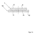
- 1a is an analyzer 1 with a circular arrangement of Shown segments 2, which together form a disc 5. Every segment consists of a blank 4 of a polarization material, the Polarization effect on absorption effects within the Polarization material is based. The direction of polarization is radial and is characterized by the reference number 3. Below the analyzer 1 there is a detector 10. which has the same number of segments 11, which are arranged in a detector chip 12. The arrangement of these segments is also circular. The segments 11 are identical and independent readable from each other. With correct adjustment everyone delivers the opposite detector segments 11 identical signals. 1a is the analyzer 1 is not yet connected to the detector 10.
- the analyzer 1 is over a transparent adhesive layer with the Detector 10 connected.
- the detector chip 12 is a hybrid signal conditioning chip 90 with attached IC amplifier modules 91 and in FIG. 1d as monolithic chip with integrated amplifier circuit 92 shown.
- 1e is a disc 5 composed of blanks 4 shown, in which the polarization direction 3 with the respective Bisector 6 of the segments 2 forms an angle ⁇ .
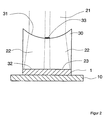
- FIG. 2 is a section through such a micropolarimeter, consisting of Analyzer 1 and detector 10 are also shown in section, with a Beam converter 30 in the form of a plano-concave lens 30 is connected upstream.
- the concave surface 31 faces the beam 21 to be analyzed while the flat surface 32 rests on the top of the analyzer 1. Due to the concave curvature of the beam converter 30 and that in the center arranged aperture 33, the beam 22 is refracted outwards, and thus from the insensitive central area of the analyzer and detector kept away. If the input beam 21 is a beam with circular cross-section, you get one on the analyzer Illuminated area 23 with a dark area in the center.
- a misalignment i.e. if the axis of the beam 21 is not parallel to the normal of the detector surface, a deformed, Illuminated area 23.
- the measured intensity of the Detector segments is detected. Based on the intensity values, a precise adjustment can be made.
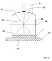
- FIG 3 is a corresponding arrangement with a plano-convex lens 40 shown.
- the flat surface 42 lies on the analyzer while the convex surface 41 facing the beam 21 to be analyzed.
- an aperture 43 is arranged in the middle.
- the curvature and the thickness of the Lens 40 is selected such that approximately in the middle between convex surface 41 and plane surface 42, the focal plane 44 extends. This ensures that the incoming rays are so strongly refracted that they affect each opposite side of the analyzer.
- This one too Arrangement gives a circularly illuminated surface 23 on the Surface of the analyzer, the center of the analyzer and thus the The center of the detector remains dark.
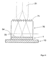
- FIG 4 shows a further embodiment with a cone 50.
- the conical surface 51 faces the beam 21 to be analyzed while the flat surface 52 rests on the surface of the analyzer.
- the level 54 in which the rays cross, runs within the cone 50, so that the incoming rays are each refracted on the opposite side become.
- an annular shape is obtained Illuminated area 23 on the top of the analyzer.
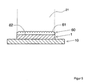
- FIG 5 shows a further embodiment by means of a lens array 60 shown.
- the lens arrangement 61 is the beam 21 to be analyzed facing, while the flat surface 62 on the top of the analyzer 1 rests.
- FIG. 6 shows a further embodiment by means of a Fresnel lens 70 shown.
- the lens surface 71 is the beam 21 to be examined facing. while the flat surface 72 on the surface of the analyzer 1 rests.
- the analyzer array has one circular arrangement of triangular segments 2, while that Detector array has rectangular segments 11 arranged next to one another.
- a beam converter 81 provided, which consists of a plurality of optical fibers 80.
- the Entry surface 82 corresponds to the shape and size of a segment of the Analyzer, while the exit surface 83 in the shape and extent of a Corresponds to segment surface 11 of the detector. This arrangement has the advantage that commercially available detector lines or detector arrays are used can be.
- FIG. 8 shows a complete Stokes meter, which in addition to Structure of Fig. 1a in front of the analyzer 1 four alternately arranged ⁇ / 4 plates 100, whose main axis direction 101 for all ⁇ / 4 platelets 100 is the same.
Landscapes
- Physics & Mathematics (AREA)
- General Physics & Mathematics (AREA)
- Spectroscopy & Molecular Physics (AREA)
- Investigating Or Analysing Materials By Optical Means (AREA)
Description
Vorzugsweise weisen jeweils gegenüberliegende Segmente dieselbe Polarisationsrichtung auf.
- Umverteilung der Intensität des Strahls im Hinblick auf eine gute Ausleuchtung des Analysators und des Detektors,
- Ausbildung eines empfindlichen Justiersignals für die Ausrichtung der Strahlachse auf die Symmetrieachse des Sensors.
- Fig. 1a
- eine perspektivische Darstellung eines Analysators und eines Detektors,
- Fig. 1b
- einen Vertikalschnitt durch den in der Fig. 1a gezeigten Analysator und Detektor,
- Fig. 1c,d
- perspektivische Darstellungen des Detektorchips,
- Fig. 1e
- einen Analysator gemäß einer weiteren Ausführungsform,
- Fig. 2
- einen Schnitt durch ein Mikropolarimeter mit einer vorgeschalteten plankonkaven Linse,
- Fig. 3
- einen Vertikalschnitt durch ein Mikropolarimeter mit einer vorgeschalteten plankonvexen Linse,
- Fig. 4
- einen Vertikalschnitt durch ein Mikropolarimeter mit einem vorgeschalteten transparenten Kegel,
- Fig. 5
- einen Vertikalschnitt durch ein Mikropolarimeter mit einem vorgeschalteten Linsenarray,
- Fig. 6
- einen Vertikalschnitt durch ein Mikropolarimeter mit einer vorgeschalteten Fresnellinse,
- Fig. 7
- die perspektivische Darstellung eines Strahlkonverters in Form eines Lichtwellenleiterbündels zwischen Analysator und Detektor, und
- Fig. 8
- ein Stokes-Meter.
Claims (24)
- Mikropolarimeter mit einem Analysator aus einem Polarisationsmaterial, bei dem die Polarisation auf Absorptionseffekten innerhalb des Materials beruht und mit einem in Strahlungsrichtung hinter dem Analysator angeordneten Detektor, der eine Anzahl ND ≥ 3 von Segmenten aufweist, wobei die Fläche des Analysators (1) größer gleich der der Segmentflächen des Detektors (10) ist, dadurch gekennzeichnet, daß der Analysator (1) eine einzige kreisförmige Anordnung von Segmenten aufweist und eine kreissymmetrische flache Scheibe bildet, wobei mindestens drei Segmente unterschiedliche Polarisation aufweisen,
daß die Analysatorscheibe (5) NA Segmente (2) aufweist mit NA = ND, und
daß in Strahlungsrichtung vor dem Analysator (1) ein Strahlkonverter angeordnet ist, um die sensitive Analysatorfläche ringförmig auszuleuchten. - Mikropolarimeter nach Anspruch 1, daduch gekennzeichnet, daß die Analysatorscheibe (5) einstückig ist und daß die Polarisationsrichtung radial oder tangential ausgerichtet ist.
- Mikropolarimeter nach Anspruch 1 oder 2, dadurch gekennzeichnet, daß jedes Segment (2) aus einem dreieckförmigen oder trapezförmigen Zuschnitt (4) des Polarisationsmaterials gebildet ist.
- Mikropolarimeter nach einem der Ansprüche 1 bis 3, dadurch gekennzeichnet, daß die Polarisationsrichtung jedes Segmentes (2) der Analysatorscheibe (5) mit der jeweiligen Winkelhalbierenden (6) des Segmentes (2) einen Winkel α bildet, für den gilt 0° ≤ α ≤ 180°.
- Mikropolarimeter nach Anspruch 4, dadurch gekennzeichnet, daß jeweils gegenüberliegende Segmente (2) dieselbe Polarisationsrichtung aufweisen.
- Mikropolarimeter nach einem der Ansprüche 1 bis 5, dadurch gekennzeichnet, daß das Polarisationsmaterial nanometergroße Teilchen mit starker Anisotropie der optischen Leitfähigkeit enthält.
- Mikropolarimeter nach einem der Ansprüche 1 bis 6, dadurch gekennzeichnet, daß das Polarisationsmaterial eine Polarisationsfolie oder ein Glas mit eingelagerten Silberteilchen ist.
- Mikropolarimeter nach einem der Ansprüche 1 bis 7, dadurch gekennzeichnet, daß die Dicke des Polarisationsmaterials im Bereich von 50 µm bis 2 mm liegt.
- Mikropolarimeter nach einem der Ansprüche 1 bis 8, dadurch gekennzeichnet, daß der Analysator (1) eine gerade Anzahl NA von Segmenten (2) aufweist.
- Mikropolarimeter nach einem der Ansprüche 1 bis 9, dadurch gekennzeichnet, daß die Zuschnitte (4) auf den Segmenten (11) des Detektors (10) mittels eines transparenten Klebers (20) befestigt sind und daß die Zuschnitte dieselbe Form aufweisen wie die Segmente (11) des Detektors (10).
- Mikropolarimeter nach einem der Ansprüche 1 bis 10, dadurch gekennzeichnet, daß die Segmente (11) des Detektors (10) rechteckig sind,
daß die Segmente (11) linear oder in Zeilen und Spalten nebeneinander angeordnet sind, und
daß zwischen den NA Segmenten (2) des Analysators (1) und den ND Segmenten (11) des Detektors (10) Lichtleiter (80) angeordnet sind. - Mikropolarimeter nach Anspruch 11, dadurch gekennzeichnet, daß pro Segment (2,11) ein verpreßtes, an die Form von Analysatorsegment (2) und Detektorsegment (11) angepaßtes Lichtleiterbündel (81) angeordnet ist.
- Mikropolarimeter nach einem der Ansprüche 1 bis 12, dadurch gekennzeichnet, daß vor mindestens zwei Analysatorsegmenten (2) jeweils ein Plättchen aus einem doppelbrechenden Material mit bekannter Phasenverschiebung δ, vorzugsweise ein λ/4-Plättchen (100), angeordnet ist.
- Mikropolarimeter nach einem der Ansprüche 1 bis 13, dadurch gekennzeichnet, daß der Strahlkonverter mindestens eine konvexe Linse (40) umfaßt.
- Mikropolarimeter nach Anspruch 14, dadurch gekennzeichnet, daß die konvexe Linse (40) eine plankonvexe Linse ist, deren plane Fläche (42) dem Analysator (1) zugewandt ist.
- Mikropolarimeter nach einem der Ansprüche 14 oder 15, dadurch gekennzeichnet, daß die plane Fläche (42) in Strahlungsrichtung hinter der Brennebene (44) liegt.
- Mikropolarimeter nach einem der Ansprüche 1 bis 13, dadurch gekennzeichnet, daß der Strahlkonverter mindestens eine konkave Linse (30) umfaßt.
- Mikropolarimeter nach Anspruch 17, dadurch gekennzeichnet, daß die konkave Linse (30) eine plankonave Linse ist, deren plane Fläche (32) dem Analysator (1) zugewandt ist.
- Mikropolarimeter nach einem der Ansprüche 1 bis 13, dadurch gekennzeichnet, daß der Strahlkonverter einen transparenten Kegel (50) umfaßt.
- Mikropolarimeter nach Anspruch 19, dadurch gekennzeichnet, daß die Neigung der Kegelfläche (51) so groß ist, daß die Grundfläche (52) des Kegels in Strahlungsrichtung hinter einer Ebene (54) liegt, in der sich die Lichtstrahlen kreuzen.
- Mikropolarimeter nach einem der Ansprüche 1 bis 13, dadurch gekennzeichnet, daß der Strahlkonverter ein Linsenarray (60), eine Fresnellinse (70) oder eine Gradientenindexlinse (73) umfaßt.
- Mikropolarimeter nach einem der Ansprüche 1 bis 21, dadurch gekennzeichnet, daß der Durchmesser des Strahlkonverters größer/gleich dem Durchmesser des Analysators (1) ist.
- Mikropolarimeter nach einem der Ansprüche 1 bis 22, dadurch gekennzeichnet, daß die Detektorsegmente (11) auf einem Signalkonditionierungschip angeordnet oder in den Signalkonditionierungschip (90) integriert sind.
- Mikropolarimeter nach einem der Ansprüche 1 bis 23, dadurch gekennzeichnet, daß der Detektor (10) ein CCD-Chip ist, dessen Pixel elektronisch zu ND Segmenten zusammengeschaltet sind.
Applications Claiming Priority (1)
| Application Number | Priority Date | Filing Date | Title |
|---|---|---|---|
| PCT/EP1997/004291 WO1999008081A1 (de) | 1997-08-06 | 1997-08-06 | Mikropolarimeter |
Publications (2)
| Publication Number | Publication Date |
|---|---|
| EP1002221A1 EP1002221A1 (de) | 2000-05-24 |
| EP1002221B1 true EP1002221B1 (de) | 2003-07-02 |
Family
ID=8166711
Family Applications (1)
| Application Number | Title | Priority Date | Filing Date |
|---|---|---|---|
| EP97938882A Expired - Lifetime EP1002221B1 (de) | 1997-08-06 | 1997-08-06 | Mikropolarimeter |
Country Status (6)
| Country | Link |
|---|---|
| US (1) | US6268915B1 (de) |
| EP (1) | EP1002221B1 (de) |
| JP (1) | JP2001512821A (de) |
| AU (1) | AU4117497A (de) |
| DE (1) | DE59710388D1 (de) |
| WO (1) | WO1999008081A1 (de) |
Families Citing this family (11)
| Publication number | Priority date | Publication date | Assignee | Title |
|---|---|---|---|---|
| US6744509B2 (en) | 2002-08-20 | 2004-06-01 | Meadowlark Optics, Inc. | Retardance sweep polarimeter and method |
| WO2005078778A1 (ja) * | 2004-02-12 | 2005-08-25 | Nikon Corporation | 照明光学装置、偏光状態検出器、露光装置及び露光方法 |
| US7304719B2 (en) * | 2004-03-31 | 2007-12-04 | Asml Holding N.V. | Patterned grid element polarizer |
| DE102005063524B4 (de) * | 2005-07-08 | 2011-01-27 | Grau, Günter, Dr. | Vorrichtung zur Messung und Erzeugung der Polarisation von Licht |
| JP5140409B2 (ja) * | 2007-12-26 | 2013-02-06 | 株式会社フォトニックラティス | 偏光計測器,測定システム |
| US20090265148A1 (en) * | 2008-04-16 | 2009-10-22 | Synopsys, Inc. | Modeling a sector-polarized-illumination source in an optical lithography system |
| US8242427B2 (en) * | 2008-08-12 | 2012-08-14 | Digital Fusion, Inc. | System and method for optically co-registering pixels |
| US8964072B2 (en) * | 2010-02-25 | 2015-02-24 | Vorotec Ltd. | Light filter with varying polarization angles and processing algorithm |
| US9295420B2 (en) * | 2014-01-29 | 2016-03-29 | Hong Kong Applied Science and Technology Research Institute Company Limited | Transmission-reflectance swappable Raman probe for physiological detections |
| EP4495578A3 (de) | 2016-10-19 | 2025-03-05 | Global Life Sciences Solutions USA LLC | Vorrichtung und verfahren zur erfassung evaneszenter wellenleiter |
| CN112763069B (zh) * | 2019-11-01 | 2023-08-29 | 锐光凯奇(镇江)光电科技有限公司 | 一种偏振光方向检测器 |
Family Cites Families (5)
| Publication number | Priority date | Publication date | Assignee | Title |
|---|---|---|---|---|
| US4286843A (en) | 1979-05-14 | 1981-09-01 | Reytblatt Zinovy V | Polariscope and filter therefor |
| GB8817382D0 (en) | 1988-07-21 | 1988-08-24 | Univ Essex | Optical polarimeter |
| DE69320623T2 (de) | 1993-06-28 | 1999-04-15 | Imm Institut Fuer Mikrotechnik Gmbh, 55129 Mainz | Mikropolarimeter, Mikrosensorsystem und Methode zum charakterisieren Dünner Filme |
| DE4442400A1 (de) | 1994-11-30 | 1996-06-05 | Imm Inst Mikrotech | Sensor zur Bestimmung der Lage im Raum |
| DE19547553C1 (de) * | 1995-12-11 | 1997-03-06 | Deutsche Forsch Luft Raumfahrt | Vorrichtung zur Bestimmung des Polarisationszustandes elektromagnetischer Strahlung |
-
1997
- 1997-08-06 US US09/485,111 patent/US6268915B1/en not_active Expired - Lifetime
- 1997-08-06 JP JP2000506507A patent/JP2001512821A/ja active Pending
- 1997-08-06 DE DE59710388T patent/DE59710388D1/de not_active Expired - Lifetime
- 1997-08-06 WO PCT/EP1997/004291 patent/WO1999008081A1/de not_active Ceased
- 1997-08-06 AU AU41174/97A patent/AU4117497A/en not_active Abandoned
- 1997-08-06 EP EP97938882A patent/EP1002221B1/de not_active Expired - Lifetime
Also Published As
| Publication number | Publication date |
|---|---|
| AU4117497A (en) | 1999-03-01 |
| EP1002221A1 (de) | 2000-05-24 |
| US6268915B1 (en) | 2001-07-31 |
| JP2001512821A (ja) | 2001-08-28 |
| WO1999008081A1 (de) | 1999-02-18 |
| DE59710388D1 (de) | 2003-08-07 |
Similar Documents
| Publication | Publication Date | Title |
|---|---|---|
| DE19842364C1 (de) | Mikropolarimeter und Ellipsometer | |
| DE69320623T2 (de) | Mikropolarimeter, Mikrosensorsystem und Methode zum charakterisieren Dünner Filme | |
| EP0011708B1 (de) | Verfahren und Vorrichtung zur Messung der Ebenheit, der Rauhigkeit oder des Krümmungsradius einer Messfläche | |
| DE3102972C2 (de) | Einrichtung zum kontinuierlichen Abtasten mittels eines Lichtflecks | |
| EP1257809B1 (de) | Spr-sensor und spr-sensoranordnung | |
| DE69416771T2 (de) | Inspektionsapparat für Halbleiterscheiben | |
| DE69226514T2 (de) | Gleichzeitiges vielfach-winkel/vielfach-wellenlängen ellipsometer und methode | |
| EP1002221B1 (de) | Mikropolarimeter | |
| EP0617273A2 (de) | Optisches Verfahren und Vorrichtung zur Analyse von Substanzen an Sensoroberflächen | |
| EP0536727A1 (de) | Multispektralsensor | |
| DE3781157T2 (de) | Buendelanalyse-vorrichtung fuer geraete zur optischen aufzeichnung. | |
| EP1484596A1 (de) | Verfahren und Vorrichtung zur dreidimensionalen Bestimmung des Brechungsindex von transparenten Schichten | |
| DE60014944T2 (de) | Vorrichtung zur bestimmung der räumlichen verteilung der spektralen emission eines objekts | |
| EP1507137B1 (de) | Verfahren und Vorrichtung zur polarisationsabhängigen und ortsaufgelösten Untersuchung einer Oberfläche oder einer Schicht | |
| DE19621512A1 (de) | Verfahren und Anordnung zur Auswertung des wellenlängenabhängigen Polarisationszustandes einer Strahlung | |
| DE1472207A1 (de) | Registriergeraet zur Messung des zirkularen Dichroismus | |
| DE69523800T2 (de) | Festpunktdetektionsvorrichtung | |
| DE69321816T2 (de) | Methode und Instrument zur Messung eines Zellenabstandes eines doppelbrechenden Teiles | |
| DE2744168C3 (de) | Magnetooptisches Spektralphotometer | |
| DE4006618C2 (de) | Vorrichtung zur Auskoppelung einer Meßstrahlung aus einem Laserstrahl | |
| DE102016008886A1 (de) | ATR-Spektrometer | |
| DE3922017C2 (de) | ||
| US4944579A (en) | Detection system for circularly polarized radiation | |
| DE69329763T2 (de) | Elektrooptische Messeinrichtung | |
| DE4201024A1 (de) | Tragbares spektralphotometer zur in situ untersuchung des absorptionsspektrums eines stoffes |
Legal Events
| Date | Code | Title | Description |
|---|---|---|---|
| PUAI | Public reference made under article 153(3) epc to a published international application that has entered the european phase |
Free format text: ORIGINAL CODE: 0009012 |
|
| 17P | Request for examination filed |
Effective date: 20000115 |
|
| AK | Designated contracting states |
Kind code of ref document: A1 Designated state(s): DE FR NL |
|
| 17Q | First examination report despatched |
Effective date: 20010315 |
|
| GRAH | Despatch of communication of intention to grant a patent |
Free format text: ORIGINAL CODE: EPIDOS IGRA |
|
| GRAH | Despatch of communication of intention to grant a patent |
Free format text: ORIGINAL CODE: EPIDOS IGRA |
|
| GRAA | (expected) grant |
Free format text: ORIGINAL CODE: 0009210 |
|
| AK | Designated contracting states |
Designated state(s): DE FR NL |
|
| REF | Corresponds to: |
Ref document number: 59710388 Country of ref document: DE Date of ref document: 20030807 Kind code of ref document: P |
|
| RAP2 | Party data changed (patent owner data changed or rights of a patent transferred) |
Owner name: NANOPHOTONICS AG |
|
| NLT2 | Nl: modifications (of names), taken from the european patent patent bulletin |
Owner name: NANOPHOTONICS AG |
|
| ET | Fr: translation filed | ||
| PLBE | No opposition filed within time limit |
Free format text: ORIGINAL CODE: 0009261 |
|
| STAA | Information on the status of an ep patent application or granted ep patent |
Free format text: STATUS: NO OPPOSITION FILED WITHIN TIME LIMIT |
|
| 26N | No opposition filed |
Effective date: 20040405 |
|
| PGFP | Annual fee paid to national office [announced via postgrant information from national office to epo] |
Ref country code: NL Payment date: 20050818 Year of fee payment: 9 |
|
| PGFP | Annual fee paid to national office [announced via postgrant information from national office to epo] |
Ref country code: FR Payment date: 20050819 Year of fee payment: 9 |
|
| PG25 | Lapsed in a contracting state [announced via postgrant information from national office to epo] |
Ref country code: NL Free format text: LAPSE BECAUSE OF NON-PAYMENT OF DUE FEES Effective date: 20070301 |
|
| NLV4 | Nl: lapsed or anulled due to non-payment of the annual fee |
Effective date: 20070301 |
|
| REG | Reference to a national code |
Ref country code: FR Ref legal event code: ST Effective date: 20080430 |
|
| PG25 | Lapsed in a contracting state [announced via postgrant information from national office to epo] |
Ref country code: FR Free format text: LAPSE BECAUSE OF NON-PAYMENT OF DUE FEES Effective date: 20070831 |
|
| PG25 | Lapsed in a contracting state [announced via postgrant information from national office to epo] |
Ref country code: FR Free format text: LAPSE BECAUSE OF NON-PAYMENT OF DUE FEES Effective date: 20060831 |
|
| PGFP | Annual fee paid to national office [announced via postgrant information from national office to epo] |
Ref country code: DE Payment date: 20090822 Year of fee payment: 13 |
|
| REG | Reference to a national code |
Ref country code: DE Ref legal event code: R119 Ref document number: 59710388 Country of ref document: DE Effective date: 20110301 |
|
| PG25 | Lapsed in a contracting state [announced via postgrant information from national office to epo] |
Ref country code: DE Free format text: LAPSE BECAUSE OF NON-PAYMENT OF DUE FEES Effective date: 20110301 |