JP2005106967A - 液晶表示装置 - Google Patents
液晶表示装置 Download PDFInfo
- Publication number
- JP2005106967A JP2005106967A JP2003337684A JP2003337684A JP2005106967A JP 2005106967 A JP2005106967 A JP 2005106967A JP 2003337684 A JP2003337684 A JP 2003337684A JP 2003337684 A JP2003337684 A JP 2003337684A JP 2005106967 A JP2005106967 A JP 2005106967A
- Authority
- JP
- Japan
- Prior art keywords
- liquid crystal
- common electrode
- electrode
- pixel electrode
- substrate
- Prior art date
- Legal status (The legal status is an assumption and is not a legal conclusion. Google has not performed a legal analysis and makes no representation as to the accuracy of the status listed.)
- Granted
Links
Images


Classifications
-
- G—PHYSICS
- G02—OPTICS
- G02F—OPTICAL DEVICES OR ARRANGEMENTS FOR THE CONTROL OF LIGHT BY MODIFICATION OF THE OPTICAL PROPERTIES OF THE MEDIA OF THE ELEMENTS INVOLVED THEREIN; NON-LINEAR OPTICS; FREQUENCY-CHANGING OF LIGHT; OPTICAL LOGIC ELEMENTS; OPTICAL ANALOGUE/DIGITAL CONVERTERS
- G02F1/00—Devices or arrangements for the control of the intensity, colour, phase, polarisation or direction of light arriving from an independent light source, e.g. switching, gating or modulating; Non-linear optics
- G02F1/01—Devices or arrangements for the control of the intensity, colour, phase, polarisation or direction of light arriving from an independent light source, e.g. switching, gating or modulating; Non-linear optics for the control of the intensity, phase, polarisation or colour
- G02F1/13—Devices or arrangements for the control of the intensity, colour, phase, polarisation or direction of light arriving from an independent light source, e.g. switching, gating or modulating; Non-linear optics for the control of the intensity, phase, polarisation or colour based on liquid crystals, e.g. single liquid crystal display cells
- G02F1/133—Constructional arrangements; Operation of liquid crystal cells; Circuit arrangements
- G02F1/1333—Constructional arrangements; Manufacturing methods
- G02F1/1343—Electrodes
- G02F1/134309—Electrodes characterised by their geometrical arrangement
- G02F1/134363—Electrodes characterised by their geometrical arrangement for applying an electric field parallel to the substrate, i.e. in-plane switching [IPS]
-
- G—PHYSICS
- G02—OPTICS
- G02F—OPTICAL DEVICES OR ARRANGEMENTS FOR THE CONTROL OF LIGHT BY MODIFICATION OF THE OPTICAL PROPERTIES OF THE MEDIA OF THE ELEMENTS INVOLVED THEREIN; NON-LINEAR OPTICS; FREQUENCY-CHANGING OF LIGHT; OPTICAL LOGIC ELEMENTS; OPTICAL ANALOGUE/DIGITAL CONVERTERS
- G02F1/00—Devices or arrangements for the control of the intensity, colour, phase, polarisation or direction of light arriving from an independent light source, e.g. switching, gating or modulating; Non-linear optics
- G02F1/01—Devices or arrangements for the control of the intensity, colour, phase, polarisation or direction of light arriving from an independent light source, e.g. switching, gating or modulating; Non-linear optics for the control of the intensity, phase, polarisation or colour
- G02F1/13—Devices or arrangements for the control of the intensity, colour, phase, polarisation or direction of light arriving from an independent light source, e.g. switching, gating or modulating; Non-linear optics for the control of the intensity, phase, polarisation or colour based on liquid crystals, e.g. single liquid crystal display cells
- G02F1/133—Constructional arrangements; Operation of liquid crystal cells; Circuit arrangements
- G02F1/1333—Constructional arrangements; Manufacturing methods
- G02F1/1335—Structural association of cells with optical devices, e.g. polarisers or reflectors
- G02F1/133553—Reflecting elements
- G02F1/133555—Transflectors
Landscapes
- Physics & Mathematics (AREA)
- Nonlinear Science (AREA)
- Geometry (AREA)
- Mathematical Physics (AREA)
- Chemical & Material Sciences (AREA)
- Crystallography & Structural Chemistry (AREA)
- General Physics & Mathematics (AREA)
- Optics & Photonics (AREA)
- Liquid Crystal (AREA)
Abstract
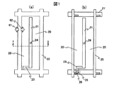
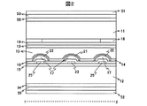
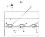
【解決手段】 櫛歯電極(21,22)で液晶層に横電界を印加するIPS(In Plane Switching)方式液晶表示装置において、櫛歯電極は光反射性でかつ間隙部(20)より突出した構造とし、櫛歯電極の断面を曲面状とする。
【効果】 櫛歯電極(21,22)の断面を曲面状とすることにより、櫛歯電極上の横電界成分が増大して櫛歯電極上の液晶を駆動することが可能になり、また、拡散反射光が増大し、IPS方式の広視野角の透過表示に加えて反射表示が可能になる。
【選択図】 図1
Description
S2=2ExEycosδ/(Ex2+Ey2)
S3=2ExEysinδ/(Ex2+Ey2)
2θPH1=225°+θLC………(1)
2θPH1=−45°+θLC………(2)
本実施例では(2)式を用い、θPH1=15°、θLC=75°とした。
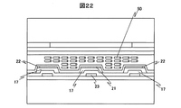
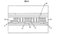
このときの液晶分子50の配向状態を図23に示す。共通電極22と画素電極21の上部に電気力線が存在しないことを反映して、同部において液晶分子50はほとんど配向変化しておらず、電圧無印加時を示す図22とほぼ同様の配向状態である。反射表示部である共通電極22と画素電極21の上部は、電圧無印加時、電圧印加時とも常に暗表示のままであり、反射率にはほとんど変化が生じない。
Nz=(nx−nz)/(nx−ny) ………(3)
Claims (13)
- 第一の基板と第二の基板と液晶層と駆動手段から主に構成され、第一の基板と第二の基板は液晶層を挟持し、第二の基板は基板面に対して平行な成分が主になるようにして液晶層に電界を印加する電圧印加手段を備えており、電圧印加手段は同一基板上に分布して櫛歯状の形状を有する画素電極と共通電極から構成され、電界は主に画素電極と共通電極の間に形成される液晶表示装置であって、
画素電極と共通電極は光反射を示し、画素電極と共通電極は両電極の間の間隙部より突出しており、画素電極と共通電極の断面は傾斜面を有する液晶表示装置。 - 画素電極と共通電極の断面は対称構造である請求項1に記載の液晶表示装置。
- 画素電極と共通電極の断面は非対称構造である請求項1に記載の液晶表示装置。
- 画素電極と共通電極の傾斜面の法線は4方向以上の方向を向く請求項1に記載の液晶表示装置。
- 画素電極と共通電極の傾斜面の法線方向が連続的に変化する請求項1に記載の液晶表示装置。
- 画素電極と共通電極は基板平面内において屈曲構造を有する請求項4に記載の液晶表示装置。
- 画素電極と共通電極の幅が一画素内において変化する請求項4に記載の液晶表示装置。
- 少なくとも隣接する画素電極と共通電極の基板平面内における形状が互いに異なる請求項4に記載の液晶表示装置。
- 画素電極と共通電極が平面方向に分布する単数又は複数の微小な突起構造を有する請求項4に記載の液晶表示装置。
- 1画素内において平面方向に分布する複数の微小な突起構造の分布は不規則性を有する請求項9に記載の液晶表示装置。
- 画素電極と共通電極が厚さ方向に分布する複数の微小な凹凸構造を有する請求項1に記載の液晶表示装置。
- 1画素内において厚さ方向に分布する複数の微小な凹凸構造の分布は不規則性を有する請求項11に記載の液晶表示装置。
- 第一の基板上に第一の基板に近接する順に第一の位相板と第一の偏光板が積層され、第二の基板上に第二の基板に近接する順に第二の位相板と第三の位相板と第二の偏光板が積層され、第一の偏光板の透過軸と第二の偏光板の透過軸は直交し、第一の位相板の遅相軸と第三の位相板の遅相軸は直交し、第二の位相板の遅相軸と透過表示部における液晶層の配向方向は直交し、第一の位相板のリタデーションと第三の位相板のリタデーションは等しく、第二の位相板のリタデーションと透過表示部における液晶層のリタデーションは等しく、第二の位相板のNz係数は0であり、第一の位相板のNz係数と第三の位相板のNz係数の一方が1で他方が0であることを特徴とする液晶表示装置。
Priority Applications (3)
| Application Number | Priority Date | Filing Date | Title |
|---|---|---|---|
| JP2003337684A JP4082683B2 (ja) | 2003-09-29 | 2003-09-29 | 半透過型液晶表示装置 |
| CNB2004100549227A CN100416386C (zh) | 2003-09-29 | 2004-07-21 | 液晶显示装置 |
| US10/953,590 US7362400B2 (en) | 2003-09-29 | 2004-09-29 | Transreflective liquid crystal display panel having a wide viewing angle |
Applications Claiming Priority (1)
| Application Number | Priority Date | Filing Date | Title |
|---|---|---|---|
| JP2003337684A JP4082683B2 (ja) | 2003-09-29 | 2003-09-29 | 半透過型液晶表示装置 |
Publications (2)
| Publication Number | Publication Date |
|---|---|
| JP2005106967A true JP2005106967A (ja) | 2005-04-21 |
| JP4082683B2 JP4082683B2 (ja) | 2008-04-30 |
Family
ID=34533442
Family Applications (1)
| Application Number | Title | Priority Date | Filing Date |
|---|---|---|---|
| JP2003337684A Expired - Fee Related JP4082683B2 (ja) | 2003-09-29 | 2003-09-29 | 半透過型液晶表示装置 |
Country Status (3)
| Country | Link |
|---|---|
| US (1) | US7362400B2 (ja) |
| JP (1) | JP4082683B2 (ja) |
| CN (1) | CN100416386C (ja) |
Cited By (37)
| Publication number | Priority date | Publication date | Assignee | Title |
|---|---|---|---|---|
| JP2005173564A (ja) * | 2003-11-21 | 2005-06-30 | Toshiba Matsushita Display Technology Co Ltd | 液晶表示装置 |
| JP2007047732A (ja) * | 2005-07-15 | 2007-02-22 | Sanyo Epson Imaging Devices Corp | 液晶表示装置及び電子機器 |
| WO2007066677A1 (en) * | 2005-12-05 | 2007-06-14 | Semiconductor Energy Laboratory Co., Ltd. | Liquid crystal display device |
| JP2007293290A (ja) * | 2006-03-27 | 2007-11-08 | Nec Corp | 液晶パネル、液晶表示装置及び端末装置 |
| JP2007334317A (ja) * | 2006-05-16 | 2007-12-27 | Semiconductor Energy Lab Co Ltd | 液晶表示装置及び半導体装置 |
| WO2008015815A1 (en) * | 2006-08-02 | 2008-02-07 | Sharp Kabushiki Kaisha | Display device |
| JP2008083220A (ja) * | 2006-09-26 | 2008-04-10 | Seiko Epson Corp | 液晶装置及び電子機器 |
| JP2008083219A (ja) * | 2006-09-26 | 2008-04-10 | Seiko Epson Corp | 液晶装置及び電子機器 |
| JP2008107687A (ja) * | 2006-10-27 | 2008-05-08 | Nec Lcd Technologies Ltd | 液晶表示装置、光学フィルムおよび端末装置 |
| JP2008151817A (ja) * | 2006-12-14 | 2008-07-03 | Hitachi Displays Ltd | 半透過型液晶表示装置 |
| JP2009075421A (ja) * | 2007-09-21 | 2009-04-09 | Epson Imaging Devices Corp | 液晶装置、及び電子機器 |
| JP2009080303A (ja) * | 2007-09-26 | 2009-04-16 | Epson Imaging Devices Corp | 液晶装置および電子機器 |
| US7525626B2 (en) | 2006-05-22 | 2009-04-28 | Mitsubishi Electric Corporation | Liquid crystal display and method for manufacturing the same |
| US7755723B2 (en) | 2006-12-25 | 2010-07-13 | Sony Corporation | Liquid crystal display device and display apparatus |
| US7773182B2 (en) | 2005-12-05 | 2010-08-10 | Semiconductor Energy Laboratory Co., Ltd. | Liquid crystal display device |
| JP2010262055A (ja) * | 2009-04-30 | 2010-11-18 | Sony Corp | 表示素子および表示装置 |
| WO2010137376A1 (ja) * | 2009-05-29 | 2010-12-02 | シャープ株式会社 | 液晶表示装置 |
| WO2011001742A1 (ja) * | 2009-07-03 | 2011-01-06 | シャープ株式会社 | 液晶表示装置 |
| JP2011138117A (ja) * | 2009-12-04 | 2011-07-14 | Semiconductor Energy Lab Co Ltd | 表示装置、及び当該表示装置を具備する電子機器 |
| JP2011180354A (ja) * | 2010-03-01 | 2011-09-15 | Hitachi Displays Ltd | 液晶表示装置 |
| JP2011237779A (ja) * | 2010-04-12 | 2011-11-24 | Semiconductor Energy Lab Co Ltd | 液晶表示装置 |
| WO2012017863A1 (ja) * | 2010-08-02 | 2012-02-09 | シャープ株式会社 | 液晶表示装置 |
| JP4882375B2 (ja) * | 2003-11-21 | 2012-02-22 | 日本ゼオン株式会社 | 液晶表示装置 |
| US8139185B2 (en) | 2006-07-07 | 2012-03-20 | Sharp Kabushiki Kaisha | Display device |
| US8208102B2 (en) | 2006-07-21 | 2012-06-26 | Sharp Kabushiki Kaisha | Display device having reflective region and transmissive region |
| US8253869B2 (en) | 2007-03-20 | 2012-08-28 | Nlt Technologies, Ltd. | Liquid crystal display device with touch panel and terminal device |
| US8338865B2 (en) | 2006-05-16 | 2012-12-25 | Semiconductor Energy Laboratory Co., Ltd. | Liquid crystal display device and semiconductor device |
| JP2013037110A (ja) * | 2011-08-05 | 2013-02-21 | Japan Display East Co Ltd | 液晶表示装置 |
| JP2013137483A (ja) * | 2011-02-18 | 2013-07-11 | Semiconductor Energy Lab Co Ltd | 液晶表示装置 |
| JP2013195992A (ja) * | 2012-03-23 | 2013-09-30 | Japan Display Inc | 液晶表示装置およびその製造方法 |
| US8687157B2 (en) | 2005-10-18 | 2014-04-01 | Semiconductor Energy Laboratory Co., Ltd. | Liquid crystal display device |
| JP2014526059A (ja) * | 2011-06-20 | 2014-10-02 | コミシリア ア レネルジ アトミック エ オ エナジーズ オルタネティヴズ | 消去電極を含む液晶表示装置 |
| US9207504B2 (en) | 2006-04-06 | 2015-12-08 | Semiconductor Energy Laboratory Co., Ltd. | Liquid crystal display device, semiconductor device, and electronic appliance |
| WO2017026480A1 (ja) * | 2015-08-11 | 2017-02-16 | シャープ株式会社 | 光学装置 |
| JPWO2018074219A1 (ja) * | 2016-10-19 | 2019-09-05 | ソニー株式会社 | 液晶表示装置および投射型表示装置 |
| JP2019179192A (ja) * | 2018-03-30 | 2019-10-17 | シチズンファインデバイス株式会社 | 照明装置、構造化照明装置及び構造化照明顕微鏡装置 |
| JP2021103320A (ja) * | 2011-11-28 | 2021-07-15 | 株式会社半導体エネルギー研究所 | 液晶表示装置 |
Families Citing this family (53)
| Publication number | Priority date | Publication date | Assignee | Title |
|---|---|---|---|---|
| KR100564219B1 (ko) | 2003-12-11 | 2006-03-28 | 엘지.필립스 엘시디 주식회사 | 횡전계형 액정표시장치용 어레이 기판 |
| TWI328708B (en) * | 2004-03-19 | 2010-08-11 | Chimei Innolux Corp | An ips liquid crystal display apparatus |
| KR100675635B1 (ko) * | 2004-05-10 | 2007-02-02 | 엘지.필립스 엘시디 주식회사 | 대조비가 향상된 횡전계모드 액정표시소자 |
| JP2006126551A (ja) * | 2004-10-29 | 2006-05-18 | Hitachi Displays Ltd | 液晶表示装置 |
| US7563490B2 (en) | 2004-12-06 | 2009-07-21 | Semiconductor Energy Laboratory Co., Ltd. | Liquid crystal display device |
| TWM281196U (en) * | 2005-04-15 | 2005-11-21 | Innolux Display Corp | A substrate and liquid crystal display device using the same |
| JP4863102B2 (ja) | 2005-06-24 | 2012-01-25 | Nltテクノロジー株式会社 | 液晶駆動電極、液晶表示装置およびその製造方法 |
| KR100685938B1 (ko) * | 2005-06-30 | 2007-02-22 | 엘지.필립스 엘시디 주식회사 | Ips모드 액정표시소자 및 그 제조방법 |
| JP4169035B2 (ja) * | 2005-07-15 | 2008-10-22 | エプソンイメージングデバイス株式会社 | 液晶装置及び電子機器 |
| DE102006057333B4 (de) * | 2005-12-30 | 2010-01-28 | Lg Display Co., Ltd. | IPS-Flüssigkristallanzeigevorrichtung |
| KR100760942B1 (ko) * | 2005-12-30 | 2007-09-21 | 엘지.필립스 엘시디 주식회사 | 횡전계형 액정 표시 장치 |
| US7847904B2 (en) | 2006-06-02 | 2010-12-07 | Semiconductor Energy Laboratory Co., Ltd. | Liquid crystal display device and electronic appliance |
| JP2008014965A (ja) * | 2006-06-30 | 2008-01-24 | Mitsubishi Electric Corp | 液晶表示装置 |
| KR101308163B1 (ko) * | 2006-06-30 | 2013-09-12 | 엘지디스플레이 주식회사 | 표시장치의 화소 전극 구조 |
| TW200809353A (en) * | 2006-07-07 | 2008-02-16 | Hitachi Displays Ltd | Optically isotropic liquid crystal materials and display apparatus using the same |
| JP4902284B2 (ja) * | 2006-07-14 | 2012-03-21 | 株式会社 日立ディスプレイズ | 半透過型液晶表示装置 |
| CN100495180C (zh) * | 2006-09-07 | 2009-06-03 | 瀚宇彩晶股份有限公司 | 液晶显示器装置 |
| JP4203676B2 (ja) * | 2006-09-27 | 2009-01-07 | カシオ計算機株式会社 | 液晶表示素子 |
| JP4889436B2 (ja) * | 2006-10-13 | 2012-03-07 | 株式会社 日立ディスプレイズ | 半透過型液晶表示装置 |
| JP4866703B2 (ja) * | 2006-10-20 | 2012-02-01 | 株式会社 日立ディスプレイズ | 液晶表示装置 |
| JP5216204B2 (ja) | 2006-10-31 | 2013-06-19 | 株式会社半導体エネルギー研究所 | 液晶表示装置及びその作製方法 |
| JP5021323B2 (ja) * | 2007-01-25 | 2012-09-05 | 東洋製罐株式会社 | 検査用容器 |
| US7751001B2 (en) * | 2007-03-21 | 2010-07-06 | Chimel Innolux Corporation | Transflective LCD with reflective layer connected to reference voltage greater than 0.5 Vrms and less than LC threshold voltage |
| KR101344874B1 (ko) | 2007-04-30 | 2013-12-26 | 삼성디스플레이 주식회사 | 액정 표시 장치 |
| US7812909B2 (en) * | 2007-04-20 | 2010-10-12 | Samsung Electronics Co., Ltd. | Liquid crystal display |
| JP4475303B2 (ja) * | 2007-08-17 | 2010-06-09 | ソニー株式会社 | 表示装置 |
| JP4488057B2 (ja) * | 2007-11-09 | 2010-06-23 | セイコーエプソン株式会社 | アクティブマトリクス装置、電気光学表示装置、および電子機器 |
| JP5241853B2 (ja) * | 2007-12-28 | 2013-07-17 | ダウ グローバル テクノロジーズ エルエルシー | 微小機能性材料 |
| US20100302487A1 (en) * | 2007-12-28 | 2010-12-02 | Storer Joey W | Phase compensation film |
| CN101526703B (zh) * | 2008-03-04 | 2011-08-17 | 上海天马微电子有限公司 | 透射反射液晶显示装置 |
| US8633879B2 (en) * | 2009-02-13 | 2014-01-21 | Apple Inc. | Undulating electrodes for improved viewing angle and color shift |
| TWI392940B (zh) * | 2009-03-11 | 2013-04-11 | Au Optronics Corp | 畫素結構、觸控式顯示面板以及液晶顯示器 |
| WO2010131552A1 (ja) * | 2009-05-13 | 2010-11-18 | シャープ株式会社 | 液晶表示装置 |
| RU2011132280A (ru) * | 2009-05-29 | 2013-07-10 | Шарп Кабушики Каиша | Элемент жидкокристаллического дисплея, жидкокристаллическое дисплейное устройство и способ отображения с помощью элемента жидкокристаллического дисплея |
| WO2011040080A1 (ja) * | 2009-09-30 | 2011-04-07 | シャープ株式会社 | 液晶表示装置 |
| CN102062978A (zh) * | 2010-11-10 | 2011-05-18 | 友达光电股份有限公司 | 液晶显示面板 |
| JP5851317B2 (ja) * | 2012-04-10 | 2016-02-03 | 株式会社ジャパンディスプレイ | 液晶表示装置 |
| CN103513473A (zh) * | 2012-06-25 | 2014-01-15 | 瀚宇彩晶股份有限公司 | 面内切换式液晶显示器之驱动电极结构 |
| US9176347B2 (en) * | 2012-12-07 | 2015-11-03 | Vastview Technology Inc. | Lateral electric field type liquid crystal display device having non-uniform spacings between two electrodes |
| TWI493265B (zh) * | 2012-12-20 | 2015-07-21 | Vastview Tech Inc | 橫向電場型液晶顯示器 |
| US9591298B2 (en) * | 2013-09-30 | 2017-03-07 | Superd Co. Ltd. | System and method for two-dimensional (2D) and three-dimensional (3D) display |
| CN103760721A (zh) | 2014-01-08 | 2014-04-30 | 北京京东方光电科技有限公司 | 薄膜晶体管阵列基板及其制备方法、显示装置 |
| JP6336762B2 (ja) * | 2014-01-24 | 2018-06-06 | 株式会社ジャパンディスプレイ | 液晶表示装置 |
| CN110780493B (zh) * | 2014-12-15 | 2022-06-07 | 群创光电股份有限公司 | 显示装置 |
| CN106324877B (zh) * | 2016-10-20 | 2019-09-20 | 京东方科技集团股份有限公司 | 显示面板、显示面板制作方法及驱动方法、显示装置 |
| US20180323239A1 (en) * | 2017-05-03 | 2018-11-08 | Innolux Corporation | Display device |
| NL2022504B1 (en) * | 2019-02-04 | 2020-08-19 | Elstar Dynamics Patents B V | Improved optical modulator |
| US11099451B1 (en) | 2020-07-31 | 2021-08-24 | Elstar Dynamics Patents B.V. | Light modulator, substrate comprising electrodes and smart glazing |
| US11099453B1 (en) | 2020-08-03 | 2021-08-24 | Elstar Dynamics Patents B.V. | Light modulator, light modulator method and smart glazing |
| CN112230466B (zh) * | 2020-10-29 | 2022-07-01 | 湖北长江新型显示产业创新中心有限公司 | 液晶光栅及其制作方法和显示装置 |
| US12007660B2 (en) | 2021-06-24 | 2024-06-11 | Elstar Dynamics Patents B.V. | Light modulator, substrate comprising electrodes and smart glazing |
| CN118632789B (zh) | 2021-12-24 | 2025-05-06 | 埃尔斯达动力专利私人有限公司 | 包括电极的基板和具有减小的衍射的光调制器 |
| CN115731854B (zh) * | 2022-11-24 | 2025-07-29 | 京东方科技集团股份有限公司 | 驱动基板、显示面板、其制作方法及显示装置 |
Family Cites Families (12)
| Publication number | Priority date | Publication date | Assignee | Title |
|---|---|---|---|---|
| DE69333323T2 (de) * | 1992-09-18 | 2004-09-16 | Hitachi, Ltd. | Flüssigkristall-Anzeigevorrichtung |
| JPH08286211A (ja) * | 1995-04-18 | 1996-11-01 | Hitachi Ltd | アクティブマトリクス型液晶表示装置 |
| JPH10142635A (ja) * | 1996-11-15 | 1998-05-29 | Furontetsuku:Kk | 液晶表示装置 |
| JP3380482B2 (ja) | 1997-12-26 | 2003-02-24 | シャープ株式会社 | 液晶表示装置 |
| TWI251697B (en) * | 1999-05-26 | 2006-03-21 | Matsushita Electric Industrial Co Ltd | Liquid crystal display element and producing method thereof |
| US6646692B2 (en) * | 2000-01-26 | 2003-11-11 | Semiconductor Energy Laboratory Co., Ltd. | Liquid-crystal display device and method of fabricating the same |
| JP3427981B2 (ja) * | 2000-07-05 | 2003-07-22 | 日本電気株式会社 | 液晶表示装置及びその製造方法 |
| JP2002040456A (ja) * | 2000-07-28 | 2002-02-06 | Nec Corp | 液晶表示装置 |
| JP2002139737A (ja) | 2000-07-31 | 2002-05-17 | Matsushita Electric Ind Co Ltd | 液晶表示装置とその製造方法 |
| JP2002350840A (ja) * | 2001-05-28 | 2002-12-04 | Hitachi Ltd | 反射型液晶表示装置 |
| EP1278097B1 (en) * | 2001-07-16 | 2006-03-01 | Hannstar Display Corporation | Electrode structure for an in-plane switching mode liquid crystal display device |
| JP4047586B2 (ja) * | 2002-01-10 | 2008-02-13 | Nec液晶テクノロジー株式会社 | 横電界方式のアクティブマトリクス型液晶表示装置 |
-
2003
- 2003-09-29 JP JP2003337684A patent/JP4082683B2/ja not_active Expired - Fee Related
-
2004
- 2004-07-21 CN CNB2004100549227A patent/CN100416386C/zh not_active Expired - Fee Related
- 2004-09-29 US US10/953,590 patent/US7362400B2/en not_active Expired - Fee Related
Cited By (97)
| Publication number | Priority date | Publication date | Assignee | Title |
|---|---|---|---|---|
| JP4882375B2 (ja) * | 2003-11-21 | 2012-02-22 | 日本ゼオン株式会社 | 液晶表示装置 |
| JP2005173564A (ja) * | 2003-11-21 | 2005-06-30 | Toshiba Matsushita Display Technology Co Ltd | 液晶表示装置 |
| JP2007047732A (ja) * | 2005-07-15 | 2007-02-22 | Sanyo Epson Imaging Devices Corp | 液晶表示装置及び電子機器 |
| US8687157B2 (en) | 2005-10-18 | 2014-04-01 | Semiconductor Energy Laboratory Co., Ltd. | Liquid crystal display device |
| US8619227B2 (en) | 2005-12-05 | 2013-12-31 | Semiconductor Energy Laboratory Co., Ltd. | Liquid crystal display device |
| US7889295B2 (en) | 2005-12-05 | 2011-02-15 | Semiconductor Energy Laboratory Co., Ltd. | Liquid crystal display device |
| US12216372B2 (en) | 2005-12-05 | 2025-02-04 | Semiconductor Energy Laboratory Co., Ltd. | Liquid crystal display device |
| US8508700B2 (en) | 2005-12-05 | 2013-08-13 | Semiconductor Energy Laboratory Co., Ltd. | Liquid crystal display device |
| US11899329B2 (en) | 2005-12-05 | 2024-02-13 | Semiconductor Energy Laboratory Co., Ltd. | Liquid crystal display device |
| US8675158B2 (en) | 2005-12-05 | 2014-03-18 | Semiconductor Energy Laboratory Co., Ltd. | Liquid crystal display device |
| US11592719B2 (en) | 2005-12-05 | 2023-02-28 | Semiconductor Energy Laboratory Co., Ltd. | Liquid crystal display device |
| WO2007066677A1 (en) * | 2005-12-05 | 2007-06-14 | Semiconductor Energy Laboratory Co., Ltd. | Liquid crystal display device |
| US11126053B2 (en) | 2005-12-05 | 2021-09-21 | Semiconductor Energy Laboratory Co., Ltd. | Liquid crystal display device |
| US9835912B2 (en) | 2005-12-05 | 2017-12-05 | Semiconductor Energy Laboratory Co., Ltd. | Liquid crystal display device |
| US11048135B2 (en) | 2005-12-05 | 2021-06-29 | Semiconductor Energy Laboratory Co., Ltd. | Liquid crystal display device |
| US8164729B2 (en) | 2005-12-05 | 2012-04-24 | Semiconductor Energy Laboratory Co., Ltd. | Liquid crystal display device |
| US7773182B2 (en) | 2005-12-05 | 2010-08-10 | Semiconductor Energy Laboratory Co., Ltd. | Liquid crystal display device |
| US10539847B2 (en) | 2005-12-05 | 2020-01-21 | Semiconductor Energy Laboratory Co., Ltd. | Liquid crystal display device |
| US10324347B1 (en) | 2005-12-05 | 2019-06-18 | Semiconductor Energy Laboratory Co., Ltd. | Liquid crystal display device |
| US10203571B2 (en) | 2005-12-05 | 2019-02-12 | Semiconductor Energy Laboratory Co., Ltd. | Liquid crystal display device |
| US10054830B2 (en) | 2005-12-05 | 2018-08-21 | Semiconductor Energy Laboratory Co., Ltd. | Liquid crystal display device |
| US7880848B2 (en) | 2005-12-05 | 2011-02-01 | Semiconductor Energy Laboratory Co., Ltd. | Liquid crystal display device |
| US7880836B2 (en) | 2005-12-05 | 2011-02-01 | Semiconductor Energy Laboratory Co., Ltd. | Liquid crystal display device |
| TWI402583B (zh) * | 2005-12-05 | 2013-07-21 | Semiconductor Energy Lab | 液晶顯示裝置及包括多個像素的液晶顯示裝置 |
| US9128336B2 (en) | 2005-12-05 | 2015-09-08 | Semiconductor Energy Laboratory Co., Ltd. | Liquid crystal display device |
| US7999892B2 (en) | 2005-12-05 | 2011-08-16 | Semiconductor Energy Laboratory Co., Ltd. | Liquid crystal display device |
| US9904127B2 (en) | 2005-12-05 | 2018-02-27 | Semiconductor Energy Laboratory Co., Ltd. | Liquid crystal display device |
| US9823526B2 (en) | 2005-12-05 | 2017-11-21 | Semiconductor Energy Laboratory Co., Ltd. | Liquid crystal display device |
| US9417492B2 (en) | 2005-12-05 | 2016-08-16 | Semiconductor Energy Laboratory Co., Ltd. | Liquid crystal display device |
| US9316881B2 (en) | 2005-12-05 | 2016-04-19 | Semiconductor Energy Laboratory Co., Ltd. | Liquid crystal display device |
| US9235090B2 (en) | 2005-12-05 | 2016-01-12 | Semiconductor Energy Laboratory Co., Ltd. | Liquid crystal display device |
| US8134663B2 (en) | 2006-03-27 | 2012-03-13 | Nlt Technologies, Ltd. | Liquid crystal panel, liquid crystal display device and terminal device |
| US8054422B2 (en) | 2006-03-27 | 2011-11-08 | Nec Lcd Technologies, Ltd | Liquid crystal display device |
| JP2007293290A (ja) * | 2006-03-27 | 2007-11-08 | Nec Corp | 液晶パネル、液晶表示装置及び端末装置 |
| US8395731B2 (en) | 2006-03-27 | 2013-03-12 | Nlt Technologies, Ltd. | Liquid crystal panel, liquid crystal display device and terminal device |
| US9213206B2 (en) | 2006-04-06 | 2015-12-15 | Semiconductor Energy Laboratory Co., Ltd. | Liquid crystal display device, semiconductor device, and electronic appliance |
| US9207504B2 (en) | 2006-04-06 | 2015-12-08 | Semiconductor Energy Laboratory Co., Ltd. | Liquid crystal display device, semiconductor device, and electronic appliance |
| US9958736B2 (en) | 2006-04-06 | 2018-05-01 | Semiconductor Energy Laboratory Co., Ltd. | Liquid crystal display device, semiconductor device, and electronic appliance |
| US10684517B2 (en) | 2006-04-06 | 2020-06-16 | Semiconductor Energy Laboratory Co., Ltd. | Liquid crystal display device, semiconductor device, and electronic appliance |
| US11073729B2 (en) | 2006-04-06 | 2021-07-27 | Semiconductor Energy Laboratory Co., Ltd. | Liquid crystal display device, semiconductor device, and electronic appliance |
| US11442317B2 (en) | 2006-04-06 | 2022-09-13 | Semiconductor Energy Laboratory Co., Ltd. | Liquid crystal display device, semiconductor device, and electronic appliance |
| US11644720B2 (en) | 2006-04-06 | 2023-05-09 | Semiconductor Energy Laboratory Co., Ltd. | Liquid crystal display device, semiconductor device, and electronic appliance |
| US11921382B2 (en) | 2006-04-06 | 2024-03-05 | Semiconductor Energy Laboratory Co., Ltd. | Liquid crystal display device, semiconductor device, and electronic appliance |
| US10509271B2 (en) | 2006-05-16 | 2019-12-17 | Semiconductor Energy Laboratory Co., Ltd. | Liquid crystal display device comprising a semiconductor film having a channel formation region overlapping with a conductive film in a floating state |
| JP2007334317A (ja) * | 2006-05-16 | 2007-12-27 | Semiconductor Energy Lab Co Ltd | 液晶表示装置及び半導体装置 |
| US9268188B2 (en) | 2006-05-16 | 2016-02-23 | Semiconductor Energy Laboratory Co., Ltd. | Liquid crystal display device and semiconductor device |
| US8841671B2 (en) | 2006-05-16 | 2014-09-23 | Semiconductor Energy Laboratory Co., Ltd. | Liquid crystal display device and semiconductor device |
| US11061285B2 (en) | 2006-05-16 | 2021-07-13 | Semiconductor Energy Laboratory Co., Ltd. | Liquid crystal display device comprising a dogleg-like shaped pixel electrode in a plane view having a plurality of dogleg-like shaped openings and semiconductor device |
| US8338865B2 (en) | 2006-05-16 | 2012-12-25 | Semiconductor Energy Laboratory Co., Ltd. | Liquid crystal display device and semiconductor device |
| US11435626B2 (en) | 2006-05-16 | 2022-09-06 | Semiconductor Energy Laboratory Co., Ltd. | Liquid crystal display device and semiconductor device |
| US10001678B2 (en) | 2006-05-16 | 2018-06-19 | Semiconductor Energy Laboratory Co., Ltd. | Liquid crystal display device and semiconductor device |
| US11106096B2 (en) | 2006-05-16 | 2021-08-31 | Semiconductor Energy Laboratory Co., Ltd. | Liquid crystal display device and semiconductor device |
| US11726371B2 (en) | 2006-05-16 | 2023-08-15 | Semiconductor Energy Laboratory Co., Ltd. | FFS-mode liquid crystal display device comprising a top-gate transistor and an auxiliary wiring connected to a common electrode in a pixel portion |
| US9709861B2 (en) | 2006-05-16 | 2017-07-18 | Semiconductor Energy Laboratory Co., Ltd. | Liquid crystal display device and semiconductor device |
| US8872182B2 (en) | 2006-05-16 | 2014-10-28 | Semiconductor Energy Laboratory Co., Ltd. | Liquid crystal display device and semiconductor device |
| US7525626B2 (en) | 2006-05-22 | 2009-04-28 | Mitsubishi Electric Corporation | Liquid crystal display and method for manufacturing the same |
| US8139185B2 (en) | 2006-07-07 | 2012-03-20 | Sharp Kabushiki Kaisha | Display device |
| US9195109B2 (en) | 2006-07-21 | 2015-11-24 | Sharp Kabushiki Kaisha | In-plane switching liquid crystal display device having reflective region and transmissive region |
| US8208102B2 (en) | 2006-07-21 | 2012-06-26 | Sharp Kabushiki Kaisha | Display device having reflective region and transmissive region |
| US8482711B2 (en) | 2006-07-21 | 2013-07-09 | Sharp Kabushiki Kaisha | In-plane switching liquid crystal display device having reflective region and transmissive region |
| JP4854740B2 (ja) * | 2006-08-02 | 2012-01-18 | シャープ株式会社 | 表示装置 |
| WO2008015815A1 (en) * | 2006-08-02 | 2008-02-07 | Sharp Kabushiki Kaisha | Display device |
| JPWO2008015815A1 (ja) * | 2006-08-02 | 2009-12-17 | シャープ株式会社 | 表示装置 |
| JP2009048213A (ja) * | 2006-08-02 | 2009-03-05 | Sharp Corp | 表示装置 |
| US8279382B2 (en) | 2006-08-02 | 2012-10-02 | Sharp Kabushiki Kaisha | Display device |
| JP2008083220A (ja) * | 2006-09-26 | 2008-04-10 | Seiko Epson Corp | 液晶装置及び電子機器 |
| JP2008083219A (ja) * | 2006-09-26 | 2008-04-10 | Seiko Epson Corp | 液晶装置及び電子機器 |
| US7830481B2 (en) | 2006-10-27 | 2010-11-09 | Nec Lcd Technologies, Ltd. | Liquid crystal display device with retardations of optical films and liquid crystal layer |
| JP2008107687A (ja) * | 2006-10-27 | 2008-05-08 | Nec Lcd Technologies Ltd | 液晶表示装置、光学フィルムおよび端末装置 |
| JP2008151817A (ja) * | 2006-12-14 | 2008-07-03 | Hitachi Displays Ltd | 半透過型液晶表示装置 |
| US7755723B2 (en) | 2006-12-25 | 2010-07-13 | Sony Corporation | Liquid crystal display device and display apparatus |
| US8253869B2 (en) | 2007-03-20 | 2012-08-28 | Nlt Technologies, Ltd. | Liquid crystal display device with touch panel and terminal device |
| JP2009075421A (ja) * | 2007-09-21 | 2009-04-09 | Epson Imaging Devices Corp | 液晶装置、及び電子機器 |
| JP2009080303A (ja) * | 2007-09-26 | 2009-04-16 | Epson Imaging Devices Corp | 液晶装置および電子機器 |
| JP2010262055A (ja) * | 2009-04-30 | 2010-11-18 | Sony Corp | 表示素子および表示装置 |
| WO2010137376A1 (ja) * | 2009-05-29 | 2010-12-02 | シャープ株式会社 | 液晶表示装置 |
| CN102282505A (zh) * | 2009-05-29 | 2011-12-14 | 夏普株式会社 | 液晶显示装置 |
| WO2011001742A1 (ja) * | 2009-07-03 | 2011-01-06 | シャープ株式会社 | 液晶表示装置 |
| JP2011138117A (ja) * | 2009-12-04 | 2011-07-14 | Semiconductor Energy Lab Co Ltd | 表示装置、及び当該表示装置を具備する電子機器 |
| JP2011180354A (ja) * | 2010-03-01 | 2011-09-15 | Hitachi Displays Ltd | 液晶表示装置 |
| JP2011237779A (ja) * | 2010-04-12 | 2011-11-24 | Semiconductor Energy Lab Co Ltd | 液晶表示装置 |
| JP2015163980A (ja) * | 2010-04-12 | 2015-09-10 | 株式会社半導体エネルギー研究所 | 液晶表示装置 |
| WO2012017863A1 (ja) * | 2010-08-02 | 2012-02-09 | シャープ株式会社 | 液晶表示装置 |
| JP2013137483A (ja) * | 2011-02-18 | 2013-07-11 | Semiconductor Energy Lab Co Ltd | 液晶表示装置 |
| JP2014526059A (ja) * | 2011-06-20 | 2014-10-02 | コミシリア ア レネルジ アトミック エ オ エナジーズ オルタネティヴズ | 消去電極を含む液晶表示装置 |
| JP2013037110A (ja) * | 2011-08-05 | 2013-02-21 | Japan Display East Co Ltd | 液晶表示装置 |
| JP7395694B2 (ja) | 2011-11-28 | 2023-12-11 | 株式会社半導体エネルギー研究所 | 液晶表示装置 |
| JP2023017878A (ja) * | 2011-11-28 | 2023-02-07 | 株式会社半導体エネルギー研究所 | 液晶表示装置 |
| JP2021103320A (ja) * | 2011-11-28 | 2021-07-15 | 株式会社半導体エネルギー研究所 | 液晶表示装置 |
| JP2024035241A (ja) * | 2011-11-28 | 2024-03-13 | 株式会社半導体エネルギー研究所 | 液晶表示装置 |
| JP7532627B2 (ja) | 2011-11-28 | 2024-08-13 | 株式会社半導体エネルギー研究所 | 液晶表示装置 |
| JP2013195992A (ja) * | 2012-03-23 | 2013-09-30 | Japan Display Inc | 液晶表示装置およびその製造方法 |
| WO2017026480A1 (ja) * | 2015-08-11 | 2017-02-16 | シャープ株式会社 | 光学装置 |
| JP6991985B2 (ja) | 2016-10-19 | 2022-01-13 | ソニーグループ株式会社 | 液晶表示装置および投射型表示装置 |
| JPWO2018074219A1 (ja) * | 2016-10-19 | 2019-09-05 | ソニー株式会社 | 液晶表示装置および投射型表示装置 |
| JP7084184B2 (ja) | 2018-03-30 | 2022-06-14 | シチズンファインデバイス株式会社 | 照明装置、構造化照明装置及び構造化照明顕微鏡装置 |
| JP2019179192A (ja) * | 2018-03-30 | 2019-10-17 | シチズンファインデバイス株式会社 | 照明装置、構造化照明装置及び構造化照明顕微鏡装置 |
Also Published As
| Publication number | Publication date |
|---|---|
| US20050105033A1 (en) | 2005-05-19 |
| US7362400B2 (en) | 2008-04-22 |
| CN100416386C (zh) | 2008-09-03 |
| CN1603915A (zh) | 2005-04-06 |
| JP4082683B2 (ja) | 2008-04-30 |
Similar Documents
| Publication | Publication Date | Title |
|---|---|---|
| JP4082683B2 (ja) | 半透過型液晶表示装置 | |
| JP4813842B2 (ja) | 液晶表示装置 | |
| JP4223992B2 (ja) | 液晶表示装置 | |
| JP4223993B2 (ja) | 液晶表示装置 | |
| CN101828142B (zh) | 液晶设备 | |
| JP4225279B2 (ja) | 液晶表示装置及び電子機器 | |
| TWI284232B (en) | Liquid crystal display device | |
| JP2009104172A (ja) | 液晶表示装置 | |
| JP2006098784A (ja) | 視野角制御装置および表示装置 | |
| KR100865843B1 (ko) | 금속격자를 이용한 단일갭형 반투과형 프린지 필드 스위칭액정표시소자 | |
| JP2006091229A (ja) | 液晶表示装置 | |
| JP5332548B2 (ja) | カラーフィルタ及びそれを備えた液晶表示装置 | |
| JP2004101773A (ja) | 液晶表示装置 | |
| CN101261402B (zh) | 液晶显示器及其制造方法 | |
| JP5254477B2 (ja) | 液晶表示装置 | |
| JP4721879B2 (ja) | 液晶表示装置 | |
| WO2006101083A1 (ja) | 液晶表示装置 | |
| JP5252849B2 (ja) | 液晶表示装置 | |
| JP4912245B2 (ja) | 液晶表示装置 | |
| JP2000029021A (ja) | 反射型液晶表示装置 | |
| JP3946746B2 (ja) | 液晶表示装置 | |
| JP3946740B2 (ja) | 液晶表示装置 | |
| JP3946738B2 (ja) | 液晶表示装置 | |
| JP3946741B2 (ja) | 液晶表示装置 | |
| JP3946744B2 (ja) | 液晶表示装置 |
Legal Events
| Date | Code | Title | Description |
|---|---|---|---|
| A621 | Written request for application examination |
Free format text: JAPANESE INTERMEDIATE CODE: A621 Effective date: 20050216 |
|
| A711 | Notification of change in applicant |
Free format text: JAPANESE INTERMEDIATE CODE: A711 Effective date: 20050310 |
|
| A977 | Report on retrieval |
Free format text: JAPANESE INTERMEDIATE CODE: A971007 Effective date: 20070214 |
|
| A131 | Notification of reasons for refusal |
Free format text: JAPANESE INTERMEDIATE CODE: A131 Effective date: 20070612 |
|
| A521 | Request for written amendment filed |
Free format text: JAPANESE INTERMEDIATE CODE: A523 Effective date: 20070809 |
|
| A131 | Notification of reasons for refusal |
Free format text: JAPANESE INTERMEDIATE CODE: A131 Effective date: 20071016 |
|
| A521 | Request for written amendment filed |
Free format text: JAPANESE INTERMEDIATE CODE: A523 Effective date: 20071210 |
|
| TRDD | Decision of grant or rejection written | ||
| A01 | Written decision to grant a patent or to grant a registration (utility model) |
Free format text: JAPANESE INTERMEDIATE CODE: A01 Effective date: 20080205 |
|
| A61 | First payment of annual fees (during grant procedure) |
Free format text: JAPANESE INTERMEDIATE CODE: A61 Effective date: 20080208 |
|
| R150 | Certificate of patent or registration of utility model |
Free format text: JAPANESE INTERMEDIATE CODE: R150 |
|
| FPAY | Renewal fee payment (event date is renewal date of database) |
Free format text: PAYMENT UNTIL: 20110222 Year of fee payment: 3 |
|
| S111 | Request for change of ownership or part of ownership |
Free format text: JAPANESE INTERMEDIATE CODE: R313115 Free format text: JAPANESE INTERMEDIATE CODE: R313121 |
|
| FPAY | Renewal fee payment (event date is renewal date of database) |
Free format text: PAYMENT UNTIL: 20110222 Year of fee payment: 3 |
|
| R350 | Written notification of registration of transfer |
Free format text: JAPANESE INTERMEDIATE CODE: R350 |
|
| FPAY | Renewal fee payment (event date is renewal date of database) |
Free format text: PAYMENT UNTIL: 20120222 Year of fee payment: 4 |
|
| FPAY | Renewal fee payment (event date is renewal date of database) |
Free format text: PAYMENT UNTIL: 20120222 Year of fee payment: 4 |
|
| FPAY | Renewal fee payment (event date is renewal date of database) |
Free format text: PAYMENT UNTIL: 20130222 Year of fee payment: 5 |
|
| FPAY | Renewal fee payment (event date is renewal date of database) |
Free format text: PAYMENT UNTIL: 20140222 Year of fee payment: 6 |
|
| R250 | Receipt of annual fees |
Free format text: JAPANESE INTERMEDIATE CODE: R250 |
|
| R250 | Receipt of annual fees |
Free format text: JAPANESE INTERMEDIATE CODE: R250 |
|
| R250 | Receipt of annual fees |
Free format text: JAPANESE INTERMEDIATE CODE: R250 |
|
| R250 | Receipt of annual fees |
Free format text: JAPANESE INTERMEDIATE CODE: R250 |
|
| LAPS | Cancellation because of no payment of annual fees |