JP2001044294A5 - - Google Patents
Download PDFInfo
- Publication number
- JP2001044294A5 JP2001044294A5 JP1999218503A JP21850399A JP2001044294A5 JP 2001044294 A5 JP2001044294 A5 JP 2001044294A5 JP 1999218503 A JP1999218503 A JP 1999218503A JP 21850399 A JP21850399 A JP 21850399A JP 2001044294 A5 JP2001044294 A5 JP 2001044294A5
- Authority
- JP
- Japan
- Prior art keywords
- gate
- oxide film
- gate electrode
- film
- semiconductor substrate
- Prior art date
- Legal status (The legal status is an assumption and is not a legal conclusion. Google has not performed a legal analysis and makes no representation as to the accuracy of the status listed.)
- Pending
Links
- 239000004065 semiconductor Substances 0.000 description 24
- 239000010410 layer Substances 0.000 description 20
- 239000000758 substrate Substances 0.000 description 17
- TWXTWZIUMCFMSG-UHFFFAOYSA-N nitride(3-) Chemical compound [N-3] TWXTWZIUMCFMSG-UHFFFAOYSA-N 0.000 description 12
- 230000015572 biosynthetic process Effects 0.000 description 7
- 238000005755 formation reaction Methods 0.000 description 7
- 230000000875 corresponding Effects 0.000 description 6
- 239000011229 interlayer Substances 0.000 description 4
- 229910021332 silicide Inorganic materials 0.000 description 4
- FVBUAEGBCNSCDD-UHFFFAOYSA-N silicide(4-) Chemical compound [Si-4] FVBUAEGBCNSCDD-UHFFFAOYSA-N 0.000 description 4
- 238000005530 etching Methods 0.000 description 3
- 238000004519 manufacturing process Methods 0.000 description 3
- 238000000034 method Methods 0.000 description 3
- 238000000926 separation method Methods 0.000 description 3
- BOTDANWDWHJENH-UHFFFAOYSA-N Tetraethyl orthosilicate Chemical compound CCO[Si](OCC)(OCC)OCC BOTDANWDWHJENH-UHFFFAOYSA-N 0.000 description 2
- 238000002955 isolation Methods 0.000 description 2
- 230000002950 deficient Effects 0.000 description 1
- 230000000694 effects Effects 0.000 description 1
- 150000004767 nitrides Chemical group 0.000 description 1
- 230000003647 oxidation Effects 0.000 description 1
- 238000007254 oxidation reaction Methods 0.000 description 1
- 229910021420 polycrystalline silicon Inorganic materials 0.000 description 1
- 229920005591 polysilicon Polymers 0.000 description 1
Images

Description
【請求項1】 半導体基板上に形成され、それぞれ構成の異なる複数の回路部を備えた半導体装置であって、
前記複数の回路部は、
前記半導体基板上および前記半導体基板上に配設された分離絶縁膜上の少なくとも一方に配設された第1および第2のゲート構造体と、
前記第1および第2のゲート構造体を覆う層間絶縁膜と、
前記層間絶縁膜を貫通して、前記半導体基板上および前記分離絶縁膜上の少なくとも一方に達する複数のコンタクトとを備え、
前記第1のゲート構造体は、
第1のゲート酸化膜と、
前記第1のゲート酸化膜上に形成された第1のゲート電極と、
前記第1のゲート電極上に形成された上部絶縁膜と、
前記上部絶縁膜、前記第1のゲート電極、前記第1のゲート酸化膜の側面に形成された第1のサイドウォール絶縁膜と、を備え、
前記第2のゲート構造体は、
第2のゲート酸化膜と、
前記第2のゲート酸化膜上に形成された第2のゲート電極と、
前記第2のゲート電極上に形成されたシリサイド層と、
前記シリサイド層、前記第2のゲート電極、前記第2のゲート酸化膜の側面に形成された第2のサイドウォール絶縁膜と、を備える、半導体装置。
1. A semiconductor device formed on a semiconductor substrate and provided with a plurality of circuit units having different configurations.
Wherein the plurality of circuit portions,
First and second gate structures disposed on at least one of the previous SL semiconductor substrate and the semiconductor substrate disposed on the isolation insulating film,
An interlayer insulating film covering the first and second gate structures, and
A plurality of contacts that penetrate the interlayer insulating film and reach at least one of the semiconductor substrate and the separating insulating film.
The first gate structure is
The first gate oxide film and
The first gate electrode formed on the first gate oxide film and
The upper insulating film formed on the first gate electrode and
The upper insulating film, the first gate electrode, and the first sidewall insulating film formed on the side surface of the first gate oxide film are provided.
The second gate structure is
The second gate oxide film and
The second gate electrode formed on the second gate oxide film and
The silicide layer formed on the second gate electrode and
A semiconductor device including the silicide layer, the second gate electrode, and a second sidewall insulating film formed on the side surface of the second gate oxide film.
【請求項16】 半導体基板上に形成され、それぞれ構成の異なる複数の回路部を備え、前記複数の回路部が、前記半導体基板上および前記半導体基板上に配設された分離絶縁膜上の少なくとも一方に配設された第1および第2のゲート構造体を備えた半導体装置の製造方法であって、
(a)半導体基板上に酸化膜を形成する工程と、
(b)前記酸化膜上にゲート電極層を形成する工程と、
(c)前記第1のゲート構造体の形成位置に対応した前記ゲート電極層上に、選択的に窒化膜を形成する工程と、
(d)前記窒化膜および、前記第2のゲート構造体の形成位置に対応した前記ゲート電極層上に、選択的に酸化膜のマスクを形成する工程と、
(e)前記酸化膜のマスクを用いて、前記窒化膜、前記ゲート電極層をエッチングした後、前記酸化膜のマスクおよび前記酸化膜を選択的に除去して、前記第1のゲート構造体の形成位置に対応して、第1のゲート酸化膜と、前記第1のゲート酸化膜上に形成された第1のゲート電極と、前記第1のゲート電極上に形成された上部窒化膜とを形成するとともに、前記第2のゲート構造体の形成位置に対応して、第2のゲート酸化膜と、前記第2のゲート酸化膜上に形成された第2のゲート電極とを形成する工程と、
(f)前記上部窒化膜、前記第1のゲート電極、前記第1のゲート酸化膜の側面に第1のサイドウォール窒化膜を形成して前記第1のゲート構造体を形成するとともに、前記第2のゲート電極および前記第2のゲート酸化膜の側面に第2のサイドウォール窒化膜を形成する工程と、
(g)前記第2のゲート電極の上部にシリサイド層を形成して前記第2のゲート構造体を形成する工程とを備える、半導体装置の製造方法。
16. formed on a semiconductor substrate, comprising a plurality of circuit units having different configurations, the plurality of circuit portions, before SL on the semiconductor substrate and on said isolation insulating film disposed on a semiconductor substrate A method for manufacturing a semiconductor device including a first and second gate structures arranged on at least one of them.
(a) A step of forming an oxide film on a semiconductor substrate and
(b) A step of forming a gate electrode layer on the oxide film and
(c) A step of selectively forming a nitride film on the gate electrode layer corresponding to the formation position of the first gate structure, and
(D) A step of selectively forming an oxide film mask on the nitride film and the gate electrode layer corresponding to the formation position of the second gate structure.
(e) After etching the nitride film and the gate electrode layer with the oxide film mask, the oxide film mask and the oxide film are selectively removed to obtain the first gate structure. Corresponding to the formation position, the first gate oxide film, the first gate electrode formed on the first gate oxide film, and the upper nitride film formed on the first gate electrode are formed. A step of forming the second gate oxide film and the second gate electrode formed on the second gate oxide film corresponding to the formation position of the second gate structure. ,
(f) A first sidewall nitride film is formed on the side surfaces of the upper nitride film, the first gate electrode, and the first gate oxide film to form the first gate structure, and the first gate structure is formed. A step of forming a second sidewall nitride film on the side surface of the gate electrode of 2 and the second gate oxide film, and
(g) A method for manufacturing a semiconductor device, comprising a step of forming a silicide layer on an upper portion of the second gate electrode to form the second gate structure.
【0018】
【課題を解決するための手段】
本発明に係る請求項1記載の半導体装置は、半導体基板上に形成され、それぞれ構成の異なる複数の回路部を備えた半導体装置であって、前記複数の回路部は、前記半導体基板上および前記半導体基板上に配設された分離絶縁膜上の少なくとも一方に配設された第1および第2のゲート構造体と、前記第1および第2のゲート構造体を覆う層間絶縁膜と、前記層間絶縁膜を貫通して、前記半導体基板上および前記分離絶縁膜上の少なくとも一方に達する複数のコンタクトとを備え、前記第1のゲート構造体は、第1のゲート酸化膜と、前記第1のゲート酸化膜上に形成された第1のゲート電極と、前記第1のゲート電極上に形成された上部絶縁膜と、前記上部絶縁膜、前記第1のゲート電極、前記第1のゲート酸化膜の側面に形成された第1のサイドウォール絶縁膜とを備え、前記第2のゲート構造体は、第2のゲート酸化膜と、前記第2のゲート酸化膜上に形成された第2のゲート電極と、前記第2のゲート電極上に形成されたシリサイド層と、前記シリサイド層、前記第2のゲート電極、前記第2のゲート酸化膜の側面に形成された第2のサイドウォール絶縁膜とを備えている。
0018
[Means for solving problems]
The semiconductor device according to
本発明に係る請求項16記載の半導体装置の製造方法は、半導体基板上に形成され、それぞれ構成の異なる複数の回路部を備え、前記複数の回路部が、前記半導体基板上および前記半導体基板上に配設された分離絶縁膜上の少なくとも一方に配設された第1および第2のゲート構造体を備えた半導体装置の製造方法であって、半導体基板上に酸化膜を形成する工程(a)と、前記酸化膜上にゲート電極層を形成する工程(b)と、前記第1のゲート構造体の形成位置に対応した前記ゲート電極層上に、選択的に窒化膜を形成する工程(c)と、前記窒化膜および、前記第2のゲート構造体の形成位置に対応した前記ゲート電極層上に、選択的に酸化膜のマスクを形成する工程(d)と、前記酸化膜のマスクを用いて、前記窒化膜、前記ゲート電極層をエッチングした後、前記酸化膜のマスクおよび前記酸化膜を選択的に除去して、前記第1のゲート構造体の形成位置に対応して、第1のゲート酸化膜と、前記第1のゲート酸化膜上に形成された第1のゲート電極と、前記第1のゲート電極上に形成された上部窒化膜とを形成するとともに、前記第2のゲート構造体の形成位置に対応して、第2のゲート酸化膜と、前記第2のゲート酸化膜上に形成された第2のゲート電極とを形成する工程(e)と、前記上部窒化膜、前記第1のゲート電極、前記第1のゲート酸化膜の側面に第1のサイドウォール窒化膜を形成して前記第1のゲート構造体を形成するとともに、前記第2のゲート電極および前記第2のゲート酸化膜の側面に第2のサイドウォール窒化膜を形成する工程(f)と、前記第2のゲート電極の上部にシリサイド層を形成して前記第2のゲート構造体を形成する工程(g)とを備えている。 The method according to claim 16, wherein according to the present invention is formed on a semiconductor substrate, each comprising a plurality of circuit portions having different configurations, the plurality of circuit portions, before Symbol semiconductor substrate and the semiconductor substrate A method for manufacturing a semiconductor device including a first and second gate structures arranged on at least one of the separation insulating films arranged above, wherein an oxide film is formed on the semiconductor substrate (a step of forming an oxide film on the semiconductor substrate. a), a step (b) of forming a gate electrode layer on the oxide film, and a step of selectively forming a nitride film on the gate electrode layer corresponding to the formation position of the first gate structure. (C), a step (d) of selectively forming an oxide film mask on the gate electrode layer corresponding to the forming position of the nitride film and the second gate structure, and the oxide film. After etching the nitride film and the gate electrode layer with a mask, the mask of the oxide film and the oxide film are selectively removed to correspond to the formation position of the first gate structure. The first gate oxide film, the first gate electrode formed on the first gate oxide film, and the upper nitride film formed on the first gate electrode are formed, and the second gate oxide film is formed. The step (e) of forming the second gate oxide film and the second gate electrode formed on the second gate oxide film according to the formation position of the gate structure, and the upper nitrided film. A first sidewall nitride film is formed on the side surface of the film, the first gate electrode, and the first gate oxide film to form the first gate structure, and the second gate electrode and the said The step (f) of forming the second sidewall nitride film on the side surface of the second gate oxide film, and forming the VDD layer on the upper part of the second gate electrode to form the second gate structure. It includes a step (g).
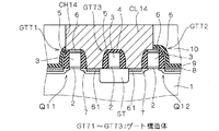
このように、サリサイド構造のゲート構造体GT34を設けることで、シェアードコンタクトによりゲート電極3とソース・ドレイン層7とを電気的に接続することが可能となり、ゲート電極3とソース・ドレイン層7との接続のための工程が簡略化できる。
Thus, by providing the
このように、STI膜ST上のゲート配線においても、ゲート電極3の上部にシリサイド層6を形成することで、ゲート構造体GT44の抵抗を下げることができ、また、シェアードコンタクトによりゲート電極3とソース・ドレイン層7とを接続することが可能となり、ゲート電極3とソース・ドレイン層7との接続のための工程が簡略化できる。
Thus, also in the gate wiring on STI film ST, by forming the
次に、図14に示す工程において、TEOS酸化膜OX2をマスクとしてポリシリコン層PS1をエッチングして酸化膜OX1を露出させる。その後、TEOS酸化膜OX2および酸化膜OX1をエッチングにより除去して、ゲート電極3およびゲート酸化膜2を成形する。
Next, in the step shown in FIG. 14, the polysilicon layer PS1 is etched with the TEOS oxide film OX2 as a mask to expose the oxide film OX1. Then, the TEOS
このような構成を採ることで、ゲート間隔(ピッチ)を短縮して高集積化を達成できる。例えば、従来、0.7μmピッチで形成していたトランジスタを、SAC構造の採用により例えば、0.56μmピッチ程度にできるが、コンタクトホールCH90を各ゲート構造体GT90間に同数で、同じように配置すると、コンタクトホールCH90が密集し、コンタクトホールCH90の形成時に、写真製版技術を用いてレジストのパターニングを行う際に、近接効果等によりパターン解像に不具合が生じる可能性がある。 By adopting such a configuration, the gate interval (pitch) can be shortened and high integration can be achieved. For example, a transistor conventionally formed at a pitch of 0.7 μm can be changed to a pitch of about 0.56 μm by adopting a SAC structure, but the same number of contact hole CH90s can be provided between the gate structures GT90 in the same manner. When arranged, the contact holes CH90 are densely packed, and when the contact holes CH90 are formed and the resist is patterned by using the photoengraving technique, there is a possibility that the pattern resolution may be defective due to the proximity effect or the like.
Priority Applications (5)
| Application Number | Priority Date | Filing Date | Title |
|---|---|---|---|
| JP11218503A JP2001044294A (en) | 1999-08-02 | 1999-08-02 | Semiconductor device and manufacture thereof |
| US09/494,785 US6299314B1 (en) | 1999-08-02 | 2000-01-31 | Semiconductor device with electrical isolation means |
| TW089109648A TW507329B (en) | 1999-08-02 | 2000-05-19 | Semiconductor device |
| KR1020000026893A KR100362336B1 (en) | 1999-08-02 | 2000-05-19 | Semiconductor device and method of manufacturing same |
| US09/927,635 US6468857B2 (en) | 1999-08-02 | 2001-08-13 | Method for forming a semiconductor device having a plurality of circuits parts |
Applications Claiming Priority (1)
| Application Number | Priority Date | Filing Date | Title |
|---|---|---|---|
| JP11218503A JP2001044294A (en) | 1999-08-02 | 1999-08-02 | Semiconductor device and manufacture thereof |
Publications (2)
| Publication Number | Publication Date |
|---|---|
| JP2001044294A JP2001044294A (en) | 2001-02-16 |
| JP2001044294A5 true JP2001044294A5 (en) | 2006-08-31 |
Family
ID=16720957
Family Applications (1)
| Application Number | Title | Priority Date | Filing Date |
|---|---|---|---|
| JP11218503A Pending JP2001044294A (en) | 1999-08-02 | 1999-08-02 | Semiconductor device and manufacture thereof |
Country Status (4)
| Country | Link |
|---|---|
| US (2) | US6299314B1 (en) |
| JP (1) | JP2001044294A (en) |
| KR (1) | KR100362336B1 (en) |
| TW (1) | TW507329B (en) |
Families Citing this family (21)
| Publication number | Priority date | Publication date | Assignee | Title |
|---|---|---|---|---|
| JP4618914B2 (en) * | 2001-03-13 | 2011-01-26 | ルネサスエレクトロニクス株式会社 | Semiconductor device |
| JP4911838B2 (en) * | 2001-07-06 | 2012-04-04 | ルネサスエレクトロニクス株式会社 | Semiconductor device and manufacturing method thereof |
| US6524938B1 (en) * | 2002-02-13 | 2003-02-25 | Taiwan Semiconductor Manufacturing Company | Method for gate formation with improved spacer profile control |
| JP4094376B2 (en) * | 2002-08-21 | 2008-06-04 | 富士通株式会社 | Semiconductor device and manufacturing method thereof |
| JP4294298B2 (en) | 2002-11-18 | 2009-07-08 | 株式会社ルネサステクノロジ | Manufacturing method of semiconductor device |
| JP2005064127A (en) * | 2003-08-08 | 2005-03-10 | Renesas Technology Corp | Semiconductor device and its manufacturing method |
| US20060108616A1 (en) * | 2004-11-22 | 2006-05-25 | Himax Technologies, Inc. | High-voltage metal-oxide-semiconductor transistor |
| US20060157819A1 (en) * | 2005-01-20 | 2006-07-20 | Bing-Chang Wu | Efuse structure |
| US20070048076A1 (en) * | 2005-08-31 | 2007-03-01 | To Chun Y | Fastening system for a ring binder mechanism |
| US7485934B2 (en) * | 2005-10-25 | 2009-02-03 | Taiwan Semiconductor Manufacturing Co., Ltd. | Integrated semiconductor structure for SRAM cells |
| JP2007214538A (en) * | 2006-01-11 | 2007-08-23 | Renesas Technology Corp | Semiconductor device, and method of manufacturing same |
| JP2008311457A (en) * | 2007-06-15 | 2008-12-25 | Renesas Technology Corp | Manufacturing method of semiconductor device |
| US20090142915A1 (en) * | 2007-12-04 | 2009-06-04 | Weize Xiong | Gate structure and method of forming the same |
| DE102008012858B4 (en) * | 2008-03-06 | 2016-08-04 | Infineon Technologies Austria Ag | Semiconductor device having an insulating trench penetrating the semiconductor device and metallic tracks for galvanically isolated signal transmission and method for its production |
| JP2010067645A (en) * | 2008-09-08 | 2010-03-25 | Renesas Technology Corp | Semiconductor device and method of manufacturing the same |
| JP2012064854A (en) * | 2010-09-17 | 2012-03-29 | Toshiba Corp | Semiconductor device |
| KR101797964B1 (en) * | 2010-10-01 | 2017-11-15 | 삼성전자주식회사 | Fabricating method of semiconductor device and the semiconductor device fabricated using the same method |
| JP2013098374A (en) * | 2011-11-01 | 2013-05-20 | Fujitsu Semiconductor Ltd | Semiconductor device manufacturing method |
| US9748232B2 (en) * | 2014-12-31 | 2017-08-29 | Taiwan Semiconductor Manufacturing Co., Ltd. | Semiconductor device structure and method for forming the same |
| KR102320047B1 (en) | 2017-07-05 | 2021-11-01 | 삼성전자주식회사 | Integrated circuit device and method of manufacturing the same |
| US11764225B2 (en) * | 2021-06-10 | 2023-09-19 | Globalfoundries U.S. Inc. | Field effect transistor with shallow trench isolation features within source/drain regions |
Family Cites Families (9)
| Publication number | Priority date | Publication date | Assignee | Title |
|---|---|---|---|---|
| JPH0923005A (en) | 1995-07-06 | 1997-01-21 | Mitsubishi Electric Corp | Semiconductor device and its manufacture |
| US6917083B1 (en) * | 1995-07-27 | 2005-07-12 | Micron Technology, Inc. | Local ground and VCC connection in an SRAM cell |
| JPH0955440A (en) | 1995-08-17 | 1997-02-25 | Sony Corp | Semiconductor device and its manufacturing method |
| JPH09326440A (en) | 1996-06-04 | 1997-12-16 | Sony Corp | Manufacture of semiconductor device |
| JP3781136B2 (en) | 1996-06-17 | 2006-05-31 | 富士通株式会社 | Semiconductor device and manufacturing method thereof |
| US5849621A (en) * | 1996-06-19 | 1998-12-15 | Advanced Micro Devices, Inc. | Method and structure for isolating semiconductor devices after transistor formation |
| US5792684A (en) * | 1997-04-21 | 1998-08-11 | Taiwan Semiconductor Manufacturing Company Ltd | Process for fabricating MOS memory devices, with a self-aligned contact structure, and MOS logic devices with salicide, both on a single semiconductor chip |
| US5863820A (en) * | 1998-02-02 | 1999-01-26 | Taiwan Semiconductor Manufacturing Company, Ltd. | Integration of sac and salicide processes on a chip having embedded memory |
| US6037222A (en) * | 1998-05-22 | 2000-03-14 | Taiwan Semiconductor Manufacturing Company | Method for fabricating a dual-gate dielectric module for memory embedded logic using salicide technology and polycide technology |
-
1999
- 1999-08-02 JP JP11218503A patent/JP2001044294A/en active Pending
-
2000
- 2000-01-31 US US09/494,785 patent/US6299314B1/en not_active Expired - Lifetime
- 2000-05-19 KR KR1020000026893A patent/KR100362336B1/en not_active IP Right Cessation
- 2000-05-19 TW TW089109648A patent/TW507329B/en not_active IP Right Cessation
-
2001
- 2001-08-13 US US09/927,635 patent/US6468857B2/en not_active Expired - Lifetime
Similar Documents
| Publication | Publication Date | Title |
|---|---|---|
| JP2001044294A5 (en) | ||
| JP2616569B2 (en) | Method for manufacturing semiconductor integrated circuit device | |
| JPH1070281A (en) | Semiconductor device and fabrication thereof | |
| US20070145491A1 (en) | Semiconductor device and method of manufacture | |
| JPH02306666A (en) | Semiconductor device and manufacture thereof | |
| TWI737258B (en) | Semiconductor structure and manufacturing method thereof | |
| US7473631B2 (en) | Method of forming contact holes in a semiconductor device having first and second metal layers | |
| JP3172998B2 (en) | Semiconductor device and manufacturing method thereof | |
| KR100474953B1 (en) | Semiconductor device and its manufacturing method | |
| KR100305402B1 (en) | Manufacturing method of semiconductor device | |
| JPH10340953A (en) | Semiconductor device | |
| KR100273314B1 (en) | Semiconductor device manufacturing method | |
| JP3688860B2 (en) | Manufacturing method of semiconductor integrated circuit | |
| JPH10326896A (en) | Semiconductor device and manufacture thereof | |
| JPH11186386A (en) | Semiconductor device and manufacture thereof | |
| JPH11274099A (en) | Semiconductor device and manufacture thereof | |
| KR100568789B1 (en) | Method for fabricating semiconductor device | |
| JP4648673B2 (en) | Semiconductor device manufacturing method, semiconductor device | |
| KR100315457B1 (en) | a manufacturing method of a semiconductor device | |
| JPH088349A (en) | Fabrication of semiconductor device | |
| KR20070065035A (en) | Manufacturing method for semiconductor device | |
| KR20030002800A (en) | Method for forming the resister polysilicon in semiconductor device | |
| JPH11145305A (en) | Manufacture of semiconductor device | |
| KR100578125B1 (en) | Method Of Patterning Interlayer Dielectric And Semiconductor Device Fabricated By Using The Method | |
| KR101001633B1 (en) | Method for forming contact hole of semiconductor device |