EP4583672A2 - Lichtemittierende vorrichtung mit einem leiterrahmen und einem isoliermaterial - Google Patents
Lichtemittierende vorrichtung mit einem leiterrahmen und einem isoliermaterial Download PDFInfo
- Publication number
- EP4583672A2 EP4583672A2 EP25169804.9A EP25169804A EP4583672A2 EP 4583672 A2 EP4583672 A2 EP 4583672A2 EP 25169804 A EP25169804 A EP 25169804A EP 4583672 A2 EP4583672 A2 EP 4583672A2
- Authority
- EP
- European Patent Office
- Prior art keywords
- lead frame
- molding
- led
- pillar
- package
- Prior art date
- Legal status (The legal status is an assumption and is not a legal conclusion. Google has not performed a legal analysis and makes no representation as to the accuracy of the status listed.)
- Pending
Links
Images


Classifications
-
- H—ELECTRICITY
- H10—SEMICONDUCTOR DEVICES; ELECTRIC SOLID-STATE DEVICES NOT OTHERWISE PROVIDED FOR
- H10H—INORGANIC LIGHT-EMITTING SEMICONDUCTOR DEVICES HAVING POTENTIAL BARRIERS
- H10H20/00—Individual inorganic light-emitting semiconductor devices having potential barriers, e.g. light-emitting diodes [LED]
- H10H20/80—Constructional details
- H10H20/85—Packages
- H10H20/857—Interconnections, e.g. lead-frames, bond wires or solder balls
-
- H—ELECTRICITY
- H10—SEMICONDUCTOR DEVICES; ELECTRIC SOLID-STATE DEVICES NOT OTHERWISE PROVIDED FOR
- H10H—INORGANIC LIGHT-EMITTING SEMICONDUCTOR DEVICES HAVING POTENTIAL BARRIERS
- H10H20/00—Individual inorganic light-emitting semiconductor devices having potential barriers, e.g. light-emitting diodes [LED]
- H10H20/01—Manufacture or treatment
- H10H20/036—Manufacture or treatment of packages
-
- H—ELECTRICITY
- H10—SEMICONDUCTOR DEVICES; ELECTRIC SOLID-STATE DEVICES NOT OTHERWISE PROVIDED FOR
- H10H—INORGANIC LIGHT-EMITTING SEMICONDUCTOR DEVICES HAVING POTENTIAL BARRIERS
- H10H20/00—Individual inorganic light-emitting semiconductor devices having potential barriers, e.g. light-emitting diodes [LED]
- H10H20/01—Manufacture or treatment
- H10H20/036—Manufacture or treatment of packages
- H10H20/0364—Manufacture or treatment of packages of interconnections
-
- H—ELECTRICITY
- H10—SEMICONDUCTOR DEVICES; ELECTRIC SOLID-STATE DEVICES NOT OTHERWISE PROVIDED FOR
- H10H—INORGANIC LIGHT-EMITTING SEMICONDUCTOR DEVICES HAVING POTENTIAL BARRIERS
- H10H20/00—Individual inorganic light-emitting semiconductor devices having potential barriers, e.g. light-emitting diodes [LED]
- H10H20/80—Constructional details
- H10H20/85—Packages
- H10H20/8506—Containers
-
- H—ELECTRICITY
- H10—SEMICONDUCTOR DEVICES; ELECTRIC SOLID-STATE DEVICES NOT OTHERWISE PROVIDED FOR
- H10H—INORGANIC LIGHT-EMITTING SEMICONDUCTOR DEVICES HAVING POTENTIAL BARRIERS
- H10H20/00—Individual inorganic light-emitting semiconductor devices having potential barriers, e.g. light-emitting diodes [LED]
- H10H20/80—Constructional details
- H10H20/85—Packages
- H10H20/852—Encapsulations
- H10H20/853—Encapsulations characterised by their shape
-
- H—ELECTRICITY
- H10—SEMICONDUCTOR DEVICES; ELECTRIC SOLID-STATE DEVICES NOT OTHERWISE PROVIDED FOR
- H10H—INORGANIC LIGHT-EMITTING SEMICONDUCTOR DEVICES HAVING POTENTIAL BARRIERS
- H10H20/00—Individual inorganic light-emitting semiconductor devices having potential barriers, e.g. light-emitting diodes [LED]
- H10H20/80—Constructional details
- H10H20/85—Packages
- H10H20/855—Optical field-shaping means, e.g. lenses
- H10H20/856—Reflecting means
-
- H—ELECTRICITY
- H10—SEMICONDUCTOR DEVICES; ELECTRIC SOLID-STATE DEVICES NOT OTHERWISE PROVIDED FOR
- H10W—GENERIC PACKAGES, INTERCONNECTIONS, CONNECTORS OR OTHER CONSTRUCTIONAL DETAILS OF DEVICES COVERED BY CLASS H10
- H10W20/00—Interconnections in chips, wafers or substrates
- H10W20/40—Interconnections external to wafers or substrates, e.g. back-end-of-line [BEOL] metallisations or vias connecting to gate electrodes
-
- H—ELECTRICITY
- H10—SEMICONDUCTOR DEVICES; ELECTRIC SOLID-STATE DEVICES NOT OTHERWISE PROVIDED FOR
- H10W—GENERIC PACKAGES, INTERCONNECTIONS, CONNECTORS OR OTHER CONSTRUCTIONAL DETAILS OF DEVICES COVERED BY CLASS H10
- H10W70/00—Package substrates; Interposers; Redistribution layers [RDL]
- H10W70/40—Leadframes
- H10W70/421—Shapes or dispositions
-
- H—ELECTRICITY
- H10—SEMICONDUCTOR DEVICES; ELECTRIC SOLID-STATE DEVICES NOT OTHERWISE PROVIDED FOR
- H10W—GENERIC PACKAGES, INTERCONNECTIONS, CONNECTORS OR OTHER CONSTRUCTIONAL DETAILS OF DEVICES COVERED BY CLASS H10
- H10W72/00—Interconnections or connectors in packages
- H10W72/50—Bond wires
- H10W72/531—Shapes of wire connectors
- H10W72/536—Shapes of wire connectors the connected ends being ball-shaped
-
- H—ELECTRICITY
- H10—SEMICONDUCTOR DEVICES; ELECTRIC SOLID-STATE DEVICES NOT OTHERWISE PROVIDED FOR
- H10W—GENERIC PACKAGES, INTERCONNECTIONS, CONNECTORS OR OTHER CONSTRUCTIONAL DETAILS OF DEVICES COVERED BY CLASS H10
- H10W72/00—Interconnections or connectors in packages
- H10W72/851—Dispositions of multiple connectors or interconnections
- H10W72/874—On different surfaces
- H10W72/884—Die-attach connectors and bond wires
-
- H—ELECTRICITY
- H10—SEMICONDUCTOR DEVICES; ELECTRIC SOLID-STATE DEVICES NOT OTHERWISE PROVIDED FOR
- H10W—GENERIC PACKAGES, INTERCONNECTIONS, CONNECTORS OR OTHER CONSTRUCTIONAL DETAILS OF DEVICES COVERED BY CLASS H10
- H10W74/00—Encapsulations, e.g. protective coatings
-
- H—ELECTRICITY
- H10—SEMICONDUCTOR DEVICES; ELECTRIC SOLID-STATE DEVICES NOT OTHERWISE PROVIDED FOR
- H10W—GENERIC PACKAGES, INTERCONNECTIONS, CONNECTORS OR OTHER CONSTRUCTIONAL DETAILS OF DEVICES COVERED BY CLASS H10
- H10W90/00—Package configurations
- H10W90/701—Package configurations characterised by the relative positions of pads or connectors relative to package parts
- H10W90/721—Package configurations characterised by the relative positions of pads or connectors relative to package parts of bump connectors
- H10W90/726—Package configurations characterised by the relative positions of pads or connectors relative to package parts of bump connectors between a chip and a stacked lead frame, conducting package substrate or heat sink
-
- H—ELECTRICITY
- H10—SEMICONDUCTOR DEVICES; ELECTRIC SOLID-STATE DEVICES NOT OTHERWISE PROVIDED FOR
- H10W—GENERIC PACKAGES, INTERCONNECTIONS, CONNECTORS OR OTHER CONSTRUCTIONAL DETAILS OF DEVICES COVERED BY CLASS H10
- H10W90/00—Package configurations
- H10W90/701—Package configurations characterised by the relative positions of pads or connectors relative to package parts
- H10W90/731—Package configurations characterised by the relative positions of pads or connectors relative to package parts of die-attach connectors
- H10W90/736—Package configurations characterised by the relative positions of pads or connectors relative to package parts of die-attach connectors between a chip and a stacked lead frame, conducting package substrate or heat sink
-
- H—ELECTRICITY
- H10—SEMICONDUCTOR DEVICES; ELECTRIC SOLID-STATE DEVICES NOT OTHERWISE PROVIDED FOR
- H10W—GENERIC PACKAGES, INTERCONNECTIONS, CONNECTORS OR OTHER CONSTRUCTIONAL DETAILS OF DEVICES COVERED BY CLASS H10
- H10W90/00—Package configurations
- H10W90/701—Package configurations characterised by the relative positions of pads or connectors relative to package parts
- H10W90/751—Package configurations characterised by the relative positions of pads or connectors relative to package parts of bond wires
- H10W90/756—Package configurations characterised by the relative positions of pads or connectors relative to package parts of bond wires between a chip and a stacked lead frame, conducting package substrate or heat sink
Definitions
- LEDs Light emitting diodes
- LEDs are solid state devices that emit light when provided with an electrical current. LEDs are packaged in a relatively complex encasement incorporating different materials to provide various functions for the LED.
- One component typically used in a package is a layer of silver.
- the silver provides good electrical conductivity to the LED semiconductor device while also providing good optical characteristics such as high reflectivity and reflectivity of light at appropriate wavelengths.
- silver is subject to tarnishing, even when covered by an encapsulation material.
- LED light emitting diode
- a package is provided herein with physical characteristics that reduce the necessity for the use of silver, which, while having good optical qualities such as reflectivity, is susceptible to being tarnished by environmental agents. More specifically, silver has a high affinity to materials such as hydrogen sulfide, halogens, oxygen, water vapor, nitrous oxide, sulfur dioxide, and ozone, which may be found in polluted air, especially in city centers or industrial areas. These materials may result in the formation of black silver sulfide or dark yellow silver oxide (known as silver tarnish), which may significantly and rapidly reduce the reflectivity of the silver.
- materials such as hydrogen sulfide, halogens, oxygen, water vapor, nitrous oxide, sulfur dioxide, and ozone, which may be found in polluted air, especially in city centers or industrial areas. These materials may result in the formation of black silver sulfide or dark yellow silver oxide (known as silver tarnish), which may significantly and rapidly reduce the reflectivity of the silver.
- the package includes a metal lead frame, a molding material disposed at least partially over the lead frame and forming a well in which light emitting diode (“LED”) components are disposed, and an encapsulation material disposed within the well.
- the metal lead frame includes pillars on which an LED or other components are disposed and/or that serve as electrical contact points to form an electrical circuit that includes the lead frame and components within the well. Areas of the lead frame other than the pillars are covered by the molding, which is optically reflective.
- the top surface of the molding material within the well is flush with (or approximately flush with) the top surface of the pillars (or the top surface of any additional layers, such as a plated metal layer or the like, formed over the pillars), to form a single flush bottom surface of the well.
- the molding material is a highly reflective material to reflect light from the LED and provide good optical characteristics for the LED package.
- the lead frame configuration having raised pillars allows a more conventional material like silver to not be used in the LED package, or to be used less in the LED package, which alleviates the silver tarnishing problem. More specifically, while in conventional designs, silver would cover much of the bottom surface of the well, and thus would be subject to tarnishing, reducing the optical characteristics of the LED package, in the package of the present disclosure, the exposed surface virtually lacks silver, reflectivity being provided by the reflective molding material not subject to silver tarnishing.
- FIG. 1 is a cross sectional view of a package 100(1) according to an example.
- the package 100 includes a lead frame 102 that includes a first lead frame part 104(a) and a second lead frame part 104(b), the first lead frame part 104(a) being electrically isolated from the second lead frame part 104(b).
- the different lead frame parts 104 of the lead frame 102 provide electrical coupling between components within the package 100 and components external to the package.
- one lead frame part 104 may couple to one terminal of an LED device 112 and to one external wire and another lead frame part 104 may couple to another terminal of the LED device 112 and to a different external wire, so that the LED device 112 is integrated into a circuit.
- a metal plating layer 106 is disposed over the first lead frame part 104(a) and the second lead frame part 104(b) in order to electrically couple various components, such as the LED 112, to the lead frame 102.
- a plating layer is made of silver so that the plating layer can perform double duty as both electrical conductor and optical reflector, in the present disclosure, the metal plating layer 106 does not need to be silver as the reflectivity of the LED package 100 is provided by the molding material 120.
- the metal plating layer 106 may be any technically feasible material other than silver, or may be silver.
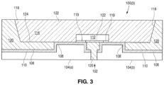
- the lead frame 102 has two raised portions or "pillars" 108 that extend above a lower surface 110 of the lead frame 102.
- the pillars 108 serve to provide points of electrical contact for electrical components (such as the LED 112) within a well 114.
- the well 114 is formed by side-walls 118 of a molding 120 made of a molding compound.
- the LED 112 is disposed on one of the pillars 108 and is electrically coupled, via a wire bond 116, to a pillar 108 of the second lead frame part 104(b).
- the LED 112 is also electrically coupled, via an electrically conductive contact 113, to the pillar 108 of the first lead frame part 104(a).
- the pillars 108 allow electrical connections to be formed between components within the well 114 and the lead frame 102 while minimizing the amount of exposed metal disposed, for example, over the lead frame 102.
- An encapsulant 122 is disposed over the components within the well 114 and fills the space of the well 114.
- the lead frame 102 with pillars 108 of the present disclosure provides the function of allowing for electrical connection of components in the well 114 to the lead frame 102 while also allowing most of the bottom-most surface of the well 114 (which bottom-most surface is also called a "basin 124") to be comprised not of silver but instead of a highly optically reflective non-electrically-conductive material.
- the basin 124 is comprised of the top-most surfaces of the metal layer 106 and of the top-most surface of the molding 120 at the bottom of the well 114. Although illustrated as being a flush surface, the various portions of the basin 124 may be slightly or substantially uneven.
- Figures 2 and 3 illustrate alternative configurations for the package 100, according to examples. More specifically, Figure 2 illustrates a package 100(2) in which the LED 112 is coupled to the lead frame 102 via two wire bonds 116 and Figure 3 illustrates a package 100(3) in which two contacts 119 on the bottom of the LED 112 couple the LED 112 to the lead frame 102.
- Figure 2 is a cross-sectional view of a package 100(2) according to another example. The package 100(2) is similar to the package 100(1) except that in the package 100(2), the LED 112 is coupled to the lead frame 102 through two wire bonds 116 (which are coupled to the LED 112 through contacts 117) instead of through a contact 113 on the bottom of the LED 112 and a single wire bond 116.
- the fillers may adjust the physical properties of the material of molding 120 to improve the integrity and reliability of the material under application conditions of the LED device, and to achieve desired optical reflectivity for the molding 120.
- the material used for the molding 120 is durable, substantially non-yellowing, mechanically suitable, compatible with appropriate manufacturing processes, and highly reflective.
- the molding 120 has a similar coefficient of thermal expansion as the lead frame 102, where "similar" means that the coefficients of thermal expansion are within 10% of each other. Although certain possible materials for the molding 120 are listed above, any suitable material may be used.
- the lead frame including the pillars 108, comprises a conductive material.
- the conductive material may be, for example, a metal such as copper, silver, gold, nickel, palladium, combinations thereof, alloys thereof, multi-layer stacks of the same or different metals, or any other suitable material.
- An encapsulant 122 is shown disposed within the well 114.
- the encapsulant 122 comprises a transparent material that protects the LED 112 and other components within the well 144, such as the wire bond 116 if present.
- the encapsulant 122 includes materials such as wavelength converting materials, materials that improve the thermal performance of the encapsulant 122, materials that cause or reduce light scattering, materials that act as filters, or any other suitable materials.
- the LED 112 may be replaced with other types of light emitting devices such as laser diodes and semiconductor light emitting devices made from other materials systems such as other III-V materials, III-phosphide, III-arsenide, II-VI materials, ZnO, or Si-based materials may be used. Blue or UV emitting light emitting devices are often combined with one or more wavelength converting materials to produce different colors of light, such that combined light from the light emitting device and the wavelength converting materials appears white or any other color necessary for a given application.
- other types of light emitting devices such as laser diodes and semiconductor light emitting devices made from other materials systems such as other III-V materials, III-phosphide, III-arsenide, II-VI materials, ZnO, or Si-based materials may be used.
- Blue or UV emitting light emitting devices are often combined with one or more wavelength converting materials to produce different colors of light, such that combined light from the light emitting device and the wavelength converting materials appears white or any other color necessary for a given application.
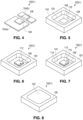
- the lead frame 102 is formed.
- the posts 108 of the lead frame 102, which are exposed after forming the molding 120, are at a higher elevation than other portions of the lead frame 102, which are covered by the molding 120 when the molding 120 is formed.
- the lead frame may be formed by, for example, shaping a sheet of metal by molding, folding, stamping, punching, etching, or any other suitable technique.
- a metal layer 106 (not shown) may be formed, for example over the entire surface of lead frame 120, or only certain locations, such as on the portions of the lead frame that are exposed after forming the molding 120.
- the metal layer 106 may be formed by plating, sputtering, evaporation, or any other suitable technique.
- the molding 120 is formed on and around the lead frame 120.
- the molding 120 may be formed by, for example, molding, injection molding, transfer molding, or any other suitable technique.
- the molding 120 may be shaped to form sidewalls 118 that form a well 114 suitable for enclosing an encapsulant 122, which is formed in Figure 8 , described below.
- a majority of the bottom surface (“basin") 124 of the well 114 is covered by the molding 120, rather than the pillars 108.
- processing steps may be taken to expose areas (such as the pillars 108) that are not to be covered by the molding 120 in the final device. Suitable processing steps include wet or dry bead blasting, chemical etching, electrolysis, or any other suitable technique to clean the surface of the pillars 108. After such cleaning, other metal layers, such as silver, gold, nickel, palladium, or other suitable materials, may be deposited on the pillars 108.
- LED 112 and any other components are attached to the pillars 108 of the lead frame that are exposed. LED 112 and other components may be attached by, for example, soldering or any other suitable technique.
- an encapsulant 122 is disposed in the well 114, covering the LED 112.
- the encapsulant 122 may be formed by, for example, molding, dispensing, or any other suitable technique.
- the encapsulant 122 is disposed in the well 114 in a liquid or gel form, then cured into a solid.
- the encapsulant 122 may include wavelength converting materials to convert the light emitted by the LED chip to light of other colors. The combination of the light from the LED chip and the light emitted from the wavelength converting materials forms the final color of the light of the LED device.
- the devices illustrated in Figures 1-8 may be used in any suitable application such as, for example, general lighting, backlighting for displays, or specialized lighting applications.
- the devices described above may be incorporated into a mobile phone.
Landscapes
- Led Device Packages (AREA)
Applications Claiming Priority (4)
| Application Number | Priority Date | Filing Date | Title |
|---|---|---|---|
| US15/652,603 US10381534B2 (en) | 2017-07-18 | 2017-07-18 | Light emitting device including a lead frame and an insulating material |
| EP17184498 | 2017-08-02 | ||
| PCT/US2018/041774 WO2019018193A1 (en) | 2017-07-18 | 2018-07-12 | LIGHT EMITTING DEVICE COMPRISING A CONNECTION GRID AND INSULATING MATERIAL |
| EP18747087.7A EP3656001A1 (de) | 2017-07-18 | 2018-07-12 | Lichtemittierende vorrichtung mit leiterrahmen und isolierendem material |
Related Parent Applications (1)
| Application Number | Title | Priority Date | Filing Date |
|---|---|---|---|
| EP18747087.7A Division EP3656001A1 (de) | 2017-07-18 | 2018-07-12 | Lichtemittierende vorrichtung mit leiterrahmen und isolierendem material |
Publications (2)
| Publication Number | Publication Date |
|---|---|
| EP4583672A2 true EP4583672A2 (de) | 2025-07-09 |
| EP4583672A3 EP4583672A3 (de) | 2025-09-24 |
Family
ID=63047471
Family Applications (2)
| Application Number | Title | Priority Date | Filing Date |
|---|---|---|---|
| EP18747087.7A Ceased EP3656001A1 (de) | 2017-07-18 | 2018-07-12 | Lichtemittierende vorrichtung mit leiterrahmen und isolierendem material |
| EP25169804.9A Pending EP4583672A3 (de) | 2017-07-18 | 2018-07-12 | Lichtemittierende vorrichtung mit einem leiterrahmen und einem isoliermaterial |
Family Applications Before (1)
| Application Number | Title | Priority Date | Filing Date |
|---|---|---|---|
| EP18747087.7A Ceased EP3656001A1 (de) | 2017-07-18 | 2018-07-12 | Lichtemittierende vorrichtung mit leiterrahmen und isolierendem material |
Country Status (6)
| Country | Link |
|---|---|
| EP (2) | EP3656001A1 (de) |
| JP (2) | JP2020527864A (de) |
| KR (1) | KR102408302B1 (de) |
| CN (1) | CN111357124A (de) |
| TW (1) | TWI832819B (de) |
| WO (1) | WO2019018193A1 (de) |
Families Citing this family (4)
| Publication number | Priority date | Publication date | Assignee | Title |
|---|---|---|---|---|
| US11335842B2 (en) * | 2018-02-14 | 2022-05-17 | Maven Optronics Co., Ltd. | Chip-scale packaging light-emitting device with electrode polarity identifier and method of manufacturing the same |
| JP2020167366A (ja) * | 2019-02-26 | 2020-10-08 | ローム株式会社 | 半導体発光装置および半導体発光装置の製造方法 |
| DE102020107409B4 (de) * | 2020-03-18 | 2023-11-02 | OSRAM Opto Semiconductors Gesellschaft mit beschränkter Haftung | Gehäuse für ein optoelektronisches halbleiterbauelement und optoelektronisches halbleiterbauelement |
| CN114628263B (zh) * | 2022-05-13 | 2022-08-05 | 威海三维曲板智能装备有限公司 | 一种光电混合封装结构及其制造方法 |
Family Cites Families (26)
| Publication number | Priority date | Publication date | Assignee | Title |
|---|---|---|---|---|
| US3830762A (en) * | 1973-08-24 | 1974-08-20 | Us Agriculture | Polysaccharide-containing elastomers |
| KR100867515B1 (ko) * | 2004-12-06 | 2008-11-07 | 삼성전기주식회사 | 발광소자 패키지 |
| US20070126020A1 (en) | 2005-12-03 | 2007-06-07 | Cheng Lin | High-power LED chip packaging structure and fabrication method thereof |
| US8044418B2 (en) * | 2006-07-13 | 2011-10-25 | Cree, Inc. | Leadframe-based packages for solid state light emitting devices |
| EP2303951B1 (de) * | 2008-07-24 | 2018-03-07 | Industrias Negromex, S.a. De C.v. | Verfahren zur herstellung von silan, hydrophobierter kieselsäure, eines kieselsäure-masterbatches und von kautschukprodukten |
| US8044420B2 (en) * | 2009-01-15 | 2011-10-25 | Advanced Semiconductor Engineering, Inc. | Light emitting diode package structure |
| KR101047603B1 (ko) * | 2009-03-10 | 2011-07-07 | 엘지이노텍 주식회사 | 발광 소자 패키지 및 그 제조방법 |
| JP2010212508A (ja) * | 2009-03-11 | 2010-09-24 | Sony Corp | 発光素子実装用パッケージ、発光装置、バックライトおよび液晶表示装置 |
| JP5509878B2 (ja) | 2010-01-27 | 2014-06-04 | 凸版印刷株式会社 | Led発光素子用リードフレーム基板の製造方法 |
| US8525213B2 (en) * | 2010-03-30 | 2013-09-03 | Lg Innotek Co., Ltd. | Light emitting device having multiple cavities and light unit having the same |
| JP5618189B2 (ja) * | 2010-07-30 | 2014-11-05 | 大日本印刷株式会社 | 樹脂付リードフレームおよびその製造方法、ならびに半導体装置およびその製造方法 |
| JP5920333B2 (ja) * | 2011-02-28 | 2016-05-18 | 日亜化学工業株式会社 | 発光装置 |
| KR101303168B1 (ko) * | 2011-07-26 | 2013-09-09 | 안상정 | 반도체 발광부 연결체 |
| JP5818149B2 (ja) * | 2011-09-09 | 2015-11-18 | 大日本印刷株式会社 | 樹脂付リードフレーム、半導体装置、照明装置、樹脂付リードフレームの製造方法および半導体装置の製造方法 |
| KR20130098048A (ko) * | 2012-02-27 | 2013-09-04 | 엘지이노텍 주식회사 | 발광소자 패키지 |
| JP2013219104A (ja) | 2012-04-05 | 2013-10-24 | Toppan Printing Co Ltd | Led用リードフレームおよびその製造方法 |
| JP5788839B2 (ja) * | 2012-08-03 | 2015-10-07 | 信越化学工業株式会社 | 硬化性樹脂組成物、その硬化物及びそれを用いた光半導体デバイス |
| CN104124237A (zh) * | 2013-04-26 | 2014-10-29 | 光明半导体(天津)有限公司 | 发光二极管封装件及其制造方法 |
| JP6176101B2 (ja) * | 2013-12-17 | 2017-08-09 | 日亜化学工業株式会社 | 樹脂パッケージ及び発光装置 |
| CN105830240B (zh) * | 2014-01-07 | 2019-11-01 | 亮锐控股有限公司 | 发光器件封装 |
| JP2017508044A (ja) * | 2014-02-27 | 2017-03-23 | イー・アイ・デュポン・ドウ・ヌムール・アンド・カンパニーE.I.Du Pont De Nemours And Company | マイクロパルプ−エラストマーマスターバッチ、及びこれに基づいた化合物 |
| JP6262578B2 (ja) * | 2014-03-18 | 2018-01-17 | スタンレー電気株式会社 | 発光装置 |
| EP3975272A1 (de) * | 2014-05-29 | 2022-03-30 | Suzhou Lekin Semiconductor Co., Ltd. | Gehäuse einer lichtemittierenden vorrichtung |
| BR112017013368B1 (pt) * | 2014-12-22 | 2021-11-23 | Nutrition & Biosciences USA 4, Inc. | Composição de mistura polimérica |
| JP6056914B2 (ja) * | 2015-07-07 | 2017-01-11 | 大日本印刷株式会社 | 樹脂付リードフレーム、半導体装置および照明装置 |
| KR102542217B1 (ko) * | 2016-10-28 | 2023-06-12 | 뉴트리션 앤드 바이오사이언시스 유에스에이 4, 인크. | 다당류를 포함하는 고무 조성물 |
-
2018
- 2018-07-12 KR KR1020207004530A patent/KR102408302B1/ko active Active
- 2018-07-12 WO PCT/US2018/041774 patent/WO2019018193A1/en not_active Ceased
- 2018-07-12 CN CN201880060567.4A patent/CN111357124A/zh active Pending
- 2018-07-12 EP EP18747087.7A patent/EP3656001A1/de not_active Ceased
- 2018-07-12 JP JP2020502262A patent/JP2020527864A/ja active Pending
- 2018-07-12 EP EP25169804.9A patent/EP4583672A3/de active Pending
- 2018-07-18 TW TW107124773A patent/TWI832819B/zh active
-
2023
- 2023-05-10 JP JP2023077765A patent/JP7605400B2/ja active Active
Also Published As
| Publication number | Publication date |
|---|---|
| EP3656001A1 (de) | 2020-05-27 |
| TWI832819B (zh) | 2024-02-21 |
| JP7605400B2 (ja) | 2024-12-24 |
| JP2020527864A (ja) | 2020-09-10 |
| CN111357124A (zh) | 2020-06-30 |
| KR102408302B1 (ko) | 2022-06-14 |
| JP2023090921A (ja) | 2023-06-29 |
| TW201916413A (zh) | 2019-04-16 |
| WO2019018193A1 (en) | 2019-01-24 |
| KR20200033889A (ko) | 2020-03-30 |
| EP4583672A3 (de) | 2025-09-24 |
Similar Documents
| Publication | Publication Date | Title |
|---|---|---|
| JP7605400B2 (ja) | リードフレーム及び絶縁材料を含む発光デバイス | |
| US8525213B2 (en) | Light emitting device having multiple cavities and light unit having the same | |
| KR101760545B1 (ko) | 수지 부착 리드 프레임 및 그 제조 방법, 및 리드 프레임 | |
| US9136453B2 (en) | Light emitting device and method of manufacturing the same | |
| CN101315963B (zh) | 半导体发光装置 | |
| US9012947B2 (en) | Light emitting diode package and method of manufacturing the same | |
| EP2378571B1 (de) | Lichtemittierende Diode | |
| US8629549B2 (en) | Carrier body for a semiconductor component, semiconductor component and method for producing a carrier body | |
| US10559728B2 (en) | Semiconductor package structure | |
| US20160118549A1 (en) | Light emitting device package | |
| US20060208364A1 (en) | LED device with flip chip structure | |
| US8487336B2 (en) | Light emitting device package | |
| US6878972B2 (en) | Light-emitting diode with plastic reflector cup | |
| US10381534B2 (en) | Light emitting device including a lead frame and an insulating material | |
| CN102769089B (zh) | 半导体封装结构 | |
| US8587016B2 (en) | Light emitting device package having light emitting device on inclined side surface and lighting system including the same | |
| KR101377603B1 (ko) | 사이드 뷰 발광 소자 패키지 및 이를 구비하는 백라이트 유닛 | |
| KR101714042B1 (ko) | 발광 소자 패키지 | |
| KR101293993B1 (ko) | 엘이디 패키지 및 이의 제조 방법 | |
| KR101911939B1 (ko) | 발광소자 패키지 | |
| US20120139002A1 (en) | Led package structure and method for manufacturing the same | |
| US10062822B1 (en) | Light-emitting diode package structure with an improved structure, light-emitting device using the same, and method of making the same | |
| KR102136373B1 (ko) | 발광소자 패키지용 리드 프레임, 리드 프레임의 제조 방법 및 발광소자 패키지의 제조 방법 | |
| KR20150080838A (ko) | 발광소자 |
Legal Events
| Date | Code | Title | Description |
|---|---|---|---|
| PUAI | Public reference made under article 153(3) epc to a published international application that has entered the european phase |
Free format text: ORIGINAL CODE: 0009012 |
|
| STAA | Information on the status of an ep patent application or granted ep patent |
Free format text: STATUS: THE APPLICATION HAS BEEN PUBLISHED |
|
| AC | Divisional application: reference to earlier application |
Ref document number: 3656001 Country of ref document: EP Kind code of ref document: P |
|
| AK | Designated contracting states |
Kind code of ref document: A2 Designated state(s): AL AT BE BG CH CY CZ DE DK EE ES FI FR GB GR HR HU IE IS IT LI LT LU LV MC MK MT NL NO PL PT RO RS SE SI SK SM TR |
|
| PUAL | Search report despatched |
Free format text: ORIGINAL CODE: 0009013 |
|
| AK | Designated contracting states |
Kind code of ref document: A3 Designated state(s): AL AT BE BG CH CY CZ DE DK EE ES FI FR GB GR HR HU IE IS IT LI LT LU LV MC MK MT NL NO PL PT RO RS SE SI SK SM TR |
|
| RIC1 | Information provided on ipc code assigned before grant |
Ipc: H10H 20/857 20250101AFI20250818BHEP Ipc: H10H 20/85 20250101ALI20250818BHEP Ipc: H10H 20/856 20250101ALN20250818BHEP |
|
| STAA | Information on the status of an ep patent application or granted ep patent |
Free format text: STATUS: REQUEST FOR EXAMINATION WAS MADE |
|
| 17P | Request for examination filed |
Effective date: 20260318 |