EP4580349A2 - Bildsensor und elektronische vorrichtung - Google Patents
Bildsensor und elektronische vorrichtung Download PDFInfo
- Publication number
- EP4580349A2 EP4580349A2 EP25173359.8A EP25173359A EP4580349A2 EP 4580349 A2 EP4580349 A2 EP 4580349A2 EP 25173359 A EP25173359 A EP 25173359A EP 4580349 A2 EP4580349 A2 EP 4580349A2
- Authority
- EP
- European Patent Office
- Prior art keywords
- wiring
- substrate
- image sensor
- pixel
- transistor
- Prior art date
- Legal status (The legal status is an assumption and is not a legal conclusion. Google has not performed a legal analysis and makes no representation as to the accuracy of the status listed.)
- Pending
Links
Images


















Classifications
-
- H—ELECTRICITY
- H10—SEMICONDUCTOR DEVICES; ELECTRIC SOLID-STATE DEVICES NOT OTHERWISE PROVIDED FOR
- H10F—INORGANIC SEMICONDUCTOR DEVICES SENSITIVE TO INFRARED RADIATION, LIGHT, ELECTROMAGNETIC RADIATION OF SHORTER WAVELENGTH OR CORPUSCULAR RADIATION
- H10F39/00—Integrated devices, or assemblies of multiple devices, comprising at least one element covered by group H10F30/00, e.g. radiation detectors comprising photodiode arrays
- H10F39/80—Constructional details of image sensors
- H10F39/813—Electronic components shared by multiple pixels, e.g. one amplifier shared by two pixels
-
- H—ELECTRICITY
- H04—ELECTRIC COMMUNICATION TECHNIQUE
- H04N—PICTORIAL COMMUNICATION, e.g. TELEVISION
- H04N25/00—Circuitry of solid-state image sensors [SSIS]; Control thereof
- H04N25/70—SSIS architectures; Circuits associated therewith
- H04N25/76—Addressed sensors, e.g. MOS or CMOS sensors
-
- H—ELECTRICITY
- H04—ELECTRIC COMMUNICATION TECHNIQUE
- H04N—PICTORIAL COMMUNICATION, e.g. TELEVISION
- H04N25/00—Circuitry of solid-state image sensors [SSIS]; Control thereof
- H04N25/70—SSIS architectures; Circuits associated therewith
- H04N25/76—Addressed sensors, e.g. MOS or CMOS sensors
- H04N25/77—Pixel circuitry, e.g. memories, A/D converters, pixel amplifiers, shared circuits or shared components
- H04N25/778—Pixel circuitry, e.g. memories, A/D converters, pixel amplifiers, shared circuits or shared components comprising amplifiers shared between a plurality of pixels, i.e. at least one part of the amplifier must be on the sensor array itself
-
- H—ELECTRICITY
- H04—ELECTRIC COMMUNICATION TECHNIQUE
- H04N—PICTORIAL COMMUNICATION, e.g. TELEVISION
- H04N25/00—Circuitry of solid-state image sensors [SSIS]; Control thereof
- H04N25/70—SSIS architectures; Circuits associated therewith
- H04N25/79—Arrangements of circuitry being divided between different or multiple substrates, chips or circuit boards, e.g. stacked image sensors
-
- H—ELECTRICITY
- H10—SEMICONDUCTOR DEVICES; ELECTRIC SOLID-STATE DEVICES NOT OTHERWISE PROVIDED FOR
- H10F—INORGANIC SEMICONDUCTOR DEVICES SENSITIVE TO INFRARED RADIATION, LIGHT, ELECTROMAGNETIC RADIATION OF SHORTER WAVELENGTH OR CORPUSCULAR RADIATION
- H10F39/00—Integrated devices, or assemblies of multiple devices, comprising at least one element covered by group H10F30/00, e.g. radiation detectors comprising photodiode arrays
- H10F39/011—Manufacture or treatment of image sensors covered by group H10F39/12
- H10F39/014—Manufacture or treatment of image sensors covered by group H10F39/12 of CMOS image sensors
-
- H—ELECTRICITY
- H10—SEMICONDUCTOR DEVICES; ELECTRIC SOLID-STATE DEVICES NOT OTHERWISE PROVIDED FOR
- H10F—INORGANIC SEMICONDUCTOR DEVICES SENSITIVE TO INFRARED RADIATION, LIGHT, ELECTROMAGNETIC RADIATION OF SHORTER WAVELENGTH OR CORPUSCULAR RADIATION
- H10F39/00—Integrated devices, or assemblies of multiple devices, comprising at least one element covered by group H10F30/00, e.g. radiation detectors comprising photodiode arrays
- H10F39/011—Manufacture or treatment of image sensors covered by group H10F39/12
- H10F39/018—Manufacture or treatment of image sensors covered by group H10F39/12 of hybrid image sensors
-
- H—ELECTRICITY
- H10—SEMICONDUCTOR DEVICES; ELECTRIC SOLID-STATE DEVICES NOT OTHERWISE PROVIDED FOR
- H10F—INORGANIC SEMICONDUCTOR DEVICES SENSITIVE TO INFRARED RADIATION, LIGHT, ELECTROMAGNETIC RADIATION OF SHORTER WAVELENGTH OR CORPUSCULAR RADIATION
- H10F39/00—Integrated devices, or assemblies of multiple devices, comprising at least one element covered by group H10F30/00, e.g. radiation detectors comprising photodiode arrays
- H10F39/10—Integrated devices
- H10F39/12—Image sensors
- H10F39/18—Complementary metal-oxide-semiconductor [CMOS] image sensors; Photodiode array image sensors
- H10F39/182—Colour image sensors
-
- H—ELECTRICITY
- H10—SEMICONDUCTOR DEVICES; ELECTRIC SOLID-STATE DEVICES NOT OTHERWISE PROVIDED FOR
- H10F—INORGANIC SEMICONDUCTOR DEVICES SENSITIVE TO INFRARED RADIATION, LIGHT, ELECTROMAGNETIC RADIATION OF SHORTER WAVELENGTH OR CORPUSCULAR RADIATION
- H10F39/00—Integrated devices, or assemblies of multiple devices, comprising at least one element covered by group H10F30/00, e.g. radiation detectors comprising photodiode arrays
- H10F39/10—Integrated devices
- H10F39/12—Image sensors
- H10F39/199—Back-illuminated image sensors
-
- H—ELECTRICITY
- H10—SEMICONDUCTOR DEVICES; ELECTRIC SOLID-STATE DEVICES NOT OTHERWISE PROVIDED FOR
- H10F—INORGANIC SEMICONDUCTOR DEVICES SENSITIVE TO INFRARED RADIATION, LIGHT, ELECTROMAGNETIC RADIATION OF SHORTER WAVELENGTH OR CORPUSCULAR RADIATION
- H10F39/00—Integrated devices, or assemblies of multiple devices, comprising at least one element covered by group H10F30/00, e.g. radiation detectors comprising photodiode arrays
- H10F39/80—Constructional details of image sensors
- H10F39/803—Pixels having integrated switching, control, storage or amplification elements
- H10F39/8037—Pixels having integrated switching, control, storage or amplification elements the integrated elements comprising a transistor
-
- H—ELECTRICITY
- H10—SEMICONDUCTOR DEVICES; ELECTRIC SOLID-STATE DEVICES NOT OTHERWISE PROVIDED FOR
- H10F—INORGANIC SEMICONDUCTOR DEVICES SENSITIVE TO INFRARED RADIATION, LIGHT, ELECTROMAGNETIC RADIATION OF SHORTER WAVELENGTH OR CORPUSCULAR RADIATION
- H10F39/00—Integrated devices, or assemblies of multiple devices, comprising at least one element covered by group H10F30/00, e.g. radiation detectors comprising photodiode arrays
- H10F39/80—Constructional details of image sensors
- H10F39/803—Pixels having integrated switching, control, storage or amplification elements
- H10F39/8037—Pixels having integrated switching, control, storage or amplification elements the integrated elements comprising a transistor
- H10F39/80373—Pixels having integrated switching, control, storage or amplification elements the integrated elements comprising a transistor characterised by the gate of the transistor
-
- H—ELECTRICITY
- H10—SEMICONDUCTOR DEVICES; ELECTRIC SOLID-STATE DEVICES NOT OTHERWISE PROVIDED FOR
- H10F—INORGANIC SEMICONDUCTOR DEVICES SENSITIVE TO INFRARED RADIATION, LIGHT, ELECTROMAGNETIC RADIATION OF SHORTER WAVELENGTH OR CORPUSCULAR RADIATION
- H10F39/00—Integrated devices, or assemblies of multiple devices, comprising at least one element covered by group H10F30/00, e.g. radiation detectors comprising photodiode arrays
- H10F39/80—Constructional details of image sensors
- H10F39/805—Coatings
- H10F39/8053—Colour filters
-
- H—ELECTRICITY
- H10—SEMICONDUCTOR DEVICES; ELECTRIC SOLID-STATE DEVICES NOT OTHERWISE PROVIDED FOR
- H10F—INORGANIC SEMICONDUCTOR DEVICES SENSITIVE TO INFRARED RADIATION, LIGHT, ELECTROMAGNETIC RADIATION OF SHORTER WAVELENGTH OR CORPUSCULAR RADIATION
- H10F39/00—Integrated devices, or assemblies of multiple devices, comprising at least one element covered by group H10F30/00, e.g. radiation detectors comprising photodiode arrays
- H10F39/80—Constructional details of image sensors
- H10F39/806—Optical elements or arrangements associated with the image sensors
-
- H—ELECTRICITY
- H10—SEMICONDUCTOR DEVICES; ELECTRIC SOLID-STATE DEVICES NOT OTHERWISE PROVIDED FOR
- H10F—INORGANIC SEMICONDUCTOR DEVICES SENSITIVE TO INFRARED RADIATION, LIGHT, ELECTROMAGNETIC RADIATION OF SHORTER WAVELENGTH OR CORPUSCULAR RADIATION
- H10F39/00—Integrated devices, or assemblies of multiple devices, comprising at least one element covered by group H10F30/00, e.g. radiation detectors comprising photodiode arrays
- H10F39/80—Constructional details of image sensors
- H10F39/806—Optical elements or arrangements associated with the image sensors
- H10F39/8063—Microlenses
-
- H—ELECTRICITY
- H10—SEMICONDUCTOR DEVICES; ELECTRIC SOLID-STATE DEVICES NOT OTHERWISE PROVIDED FOR
- H10F—INORGANIC SEMICONDUCTOR DEVICES SENSITIVE TO INFRARED RADIATION, LIGHT, ELECTROMAGNETIC RADIATION OF SHORTER WAVELENGTH OR CORPUSCULAR RADIATION
- H10F39/00—Integrated devices, or assemblies of multiple devices, comprising at least one element covered by group H10F30/00, e.g. radiation detectors comprising photodiode arrays
- H10F39/80—Constructional details of image sensors
- H10F39/807—Pixel isolation structures
-
- H—ELECTRICITY
- H10—SEMICONDUCTOR DEVICES; ELECTRIC SOLID-STATE DEVICES NOT OTHERWISE PROVIDED FOR
- H10F—INORGANIC SEMICONDUCTOR DEVICES SENSITIVE TO INFRARED RADIATION, LIGHT, ELECTROMAGNETIC RADIATION OF SHORTER WAVELENGTH OR CORPUSCULAR RADIATION
- H10F39/00—Integrated devices, or assemblies of multiple devices, comprising at least one element covered by group H10F30/00, e.g. radiation detectors comprising photodiode arrays
- H10F39/80—Constructional details of image sensors
- H10F39/809—Constructional details of image sensors of hybrid image sensors
-
- H—ELECTRICITY
- H10—SEMICONDUCTOR DEVICES; ELECTRIC SOLID-STATE DEVICES NOT OTHERWISE PROVIDED FOR
- H10F—INORGANIC SEMICONDUCTOR DEVICES SENSITIVE TO INFRARED RADIATION, LIGHT, ELECTROMAGNETIC RADIATION OF SHORTER WAVELENGTH OR CORPUSCULAR RADIATION
- H10F39/00—Integrated devices, or assemblies of multiple devices, comprising at least one element covered by group H10F30/00, e.g. radiation detectors comprising photodiode arrays
- H10F39/80—Constructional details of image sensors
- H10F39/811—Interconnections
-
- H—ELECTRICITY
- H10—SEMICONDUCTOR DEVICES; ELECTRIC SOLID-STATE DEVICES NOT OTHERWISE PROVIDED FOR
- H10F—INORGANIC SEMICONDUCTOR DEVICES SENSITIVE TO INFRARED RADIATION, LIGHT, ELECTROMAGNETIC RADIATION OF SHORTER WAVELENGTH OR CORPUSCULAR RADIATION
- H10F39/00—Integrated devices, or assemblies of multiple devices, comprising at least one element covered by group H10F30/00, e.g. radiation detectors comprising photodiode arrays
- H10F39/80—Constructional details of image sensors
- H10F39/802—Geometry or disposition of elements in pixels, e.g. address-lines or gate electrodes
Definitions
- the present disclosure relates to an image sensor and an electronic apparatus, such as a camera, provided with the image sensor.
- CMOS complementary metal-oxide-semiconductor
- Patent Document 1 JP 2010-245506 A
- the image capturing device disclosed in Patent Document 1 has a photoelectric transducer and a pixel transistor, both disposed on the same semiconductor substrate.
- the pixel transistor reads out an electric signal corresponding to the amount of light received by the photoelectric transducer.
- Such a configuration fails to reduce the area of the substrate (the space of the substrate's surface on which circuit components such as transistors are formed) satisfactorily.
- first substrate the substrate on which the photoelectric transducer is formed
- second substrate the substrate on which the pixel transistor is formed
- a plurality of photoelectric transducers having a one-to-one correspondence with a plurality of pixels shares one pixel transistor.
- elements e.g., circuit components such as transistors
- a plurality of first elements provided for respective corresponding photoelectric transducers is commonly connected to a second element to be a shared element.
- the configuration described above is necessary to connect the plurality of first elements on the first substrate to the wiring that leads to the second element shared by the first elements and formed on the second substrate, using a contact one by one. This will increase the number of contacts for the wiring, causing the area to be large.
- the present disclosure is intended to provide an image sensor and an electronic apparatus capable of reducing the substrate mounting area.
- an image sensor is an image sensor including a first substrate having a plurality of photoelectric transducers formed on the first substrate, a second substrate having a pixel transistor for each of sets of two or more of the photoelectric transducers as a constituent unit, the pixel transistor being shared by the set and formed on the second substrate, and a second wiring which is connected to a first wiring formed on the second substrate via one contact, and is connected to a plurality of first elements, the first wiring leading to a second element shared by a plurality of first elements among a plurality of elements formed on the first substrate, each of the plurality of first elements being formed for each of the photoelectric transducers.
- element used herein is a concept that includes the entirety or a part of circuit components, such as photoelectric transducers, transistors, and wirings (including electrodes), formed on a substrate (a semiconductor substrate).
- pixel transistor is a transistor that is used to read out an electric signal corresponding to the amount of light received by the photoelectric transducer and can be shared by a plurality of photoelectric transducers (pixels).
- the pixel transistor includes at least an amplification transistor that amplifies and outputs an electric signal supplied from the photoelectric transducer.
- the image sensor of the present disclosure is provided with the first wiring and the second wiring.
- the first wiring formed on the second substrate leads to the second element shared by the plurality of first elements on the first substrate.
- the second wiring is connected to the first wiring via one contact and is connected to the plurality of first elements.
- the second wiring aggregates a plurality of first elements and is connected, via one contact, to the wiring leading to the second element shared (commonly connected) by the plurality of first elements. This makes it sufficient to set the number of contacts formed in the first wiring for connecting the plurality of first elements as a constituent unit for aggregation to the first wiring to one. Thus, it is possible to reduce the number of contacts and the area of the first wiring.
- the image sensor of the present disclosure has the first substrate on which the photoelectric transducer is formed and the second substrate on which the pixel transistor is formed.
- the first substrate and the second substrate are individually stacked on top of each other. Thus, it is possible to reduce the substrate's area.
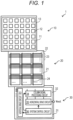
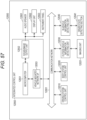
- Fig. 1 is a diagram illustrating an example of a schematic configuration of an image sensor 1 applied to each embodiment of the present disclosure.
- the image sensor 1 converts the received light into an electric signal and outputs it as a pixel signal.
- the image sensor 1 is configured as a CMOS image sensor.
- Fig. 1 illustrates an example of a schematic configuration of the image sensor 1 according to an embodiment of the present disclosure.
- the image sensor 1 includes three substrates (a first substrate 10, a second substrate 20, and a third substrate 30).
- the image sensor 1 is an image capturing device having a three-dimensional structure in which three substrates (first substrate 10, second substrate 20, and third substrate 30) are joined together.
- the first substrate 10, the second substrate 20, and the third substrate 30 are stacked in this order on top of each other.
- the first substrate 10 has a plurality of sensor pixels 12 that performs the photoelectric conversion.
- the sensor pixels 12 are disposed on a semiconductor substrate 11.
- the plurality of sensor pixels 12 is provided in a matrix in a pixel region 13 of the first substrate 10.
- the second substrate 20 has one readout circuit 22 for every four sensor pixels 12.
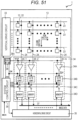
- the readout circuit 22 outputs a pixel signal based on the electric charge output from the sensor pixel 12 to a semiconductor substrate 303.
- the second substrate 20 has a plurality of pixel drive lines 23 extending in the row direction and a plurality of vertical signal lines 24 extending in the column direction.
- the third substrate 30 has a logic circuit 32 formed on a semiconductor substrate 31.
- the logic circuit 32 processes a pixel signal.
- the logic circuit 32 has, in one example, a vertical drive circuit 33, a column signal processing circuit 34, a horizontal drive circuit 35, and a system control circuit 36.
- the logic circuit 32 (specifically, the horizontal drive circuit 35 thereof) outputs the output voltage Vout for each sensor pixel 12 to the outside.
- the logic circuit 32 can have, in one example, a low-resistance region including a silicide prepared by performing a process using self-aligned silicide (salicide) such as CoSi 2 or NiSi, on the surface of the impurity diffusion region in contact with a source electrode and a drain electrode.
- silicide self-aligned silicide
- the vertical drive circuit 33 selects a plurality of sensor pixels 12, in one example, sequentially in row units.
- the column signal processing circuit 34 performs, in one example, correlated double sampling (CDS) processing on the pixel signal output from each sensor pixel 12 in the row selected by the vertical drive circuit 33.
- CDS correlated double sampling
- the column signal processing circuit 34 extracts, in one example, the signal level of the pixel signal by the CDS processing and holds pixel data corresponding to the amount of light received by each sensor pixel 12.
- the horizontal drive circuit 35 sequentially outputs, in one example, the pixel data held in the column signal processing circuit 34 to the outside.
- the system control circuit 36 controls, in one example, the driving of each block (i.e., the vertical drive circuit 33, the column signal processing circuit 34, and the horizontal drive circuit 35) in the logic circuit 32.
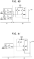
- Fig. 2 is a diagram illustrating an example of a sensor pixel 12 and a readout circuit 22. The description below is given of a case where the four sensor pixels 12 share one readout circuit 22 as illustrated in Fig. 2 .
- the term "share" used herein means that the outputs of the four sensor pixels 12 are input to the common readout circuit 22.
- the sensor pixels 12 each have a constituent component common to each other.
- an identification number i.e., 1, 2, 3, or 4
- the identification number is attached to the end of the reference numeral of the component of each sensor pixel 12.
- the identification number at the end of the reference numeral of the component of each sensor pixel 12 can be omitted.
- the sensor pixels 12 each have, in one example, a photodiode PD, a transfer transistor TR electrically connected to the photodiode PD, and a floating diffusion FD that temporarily holds the electric charge output from the photodiode PD via the transfer transistor TR.
- the photodiode PD corresponds to a specific implementation example of the "photoelectric transducer" of the present disclosure.
- the photodiode PD performs the photoelectric conversion to generate an electric charge corresponding to the amount of received light.
- the photodiode PD has the cathode electrically connected to the source of the transfer transistor TR and the anode electrically connected to the reference potential line (e.g., ground).
- the transfer transistor TR has the drain electrically connected to the floating diffusion FD and the gate electrically connected to the pixel drive line 23.
- the transfer transistor TR is, in one example, a complementary metal-oxide-semiconductor (CMOS) transistor.
- CMOS complementary metal-oxide-s
- the floating diffusion regions FDs of the sensor pixels 12 that share one readout circuit 22 are electrically connected to each other and are also electrically connected to the input terminal of the common readout circuit 22.
- the readout circuit 22 has, in one example, a reset transistor RST, a selection transistor SEL, and an amplification transistor AMP. Moreover, the selection transistor SEL can be omitted if necessary.
- the reset transistor RST has the source (the input terminal of the readout circuit 22) electrically connected to the floating diffusion FD and the drain electrically connected to a power supply line VDD and the drain of the amplification transistor AMP.
- the reset transistor RST has the gate electrically connected to the pixel drive line 23 (see Fig. 1 ).
- the amplification transistor AMP has the source electrically connected to the drain of the selection transistor SEL and the gate electrically connected to the source of the reset transistor RST.
- the selection transistor SEL (the output terminal of the readout circuit 22) has the source electrically connected to the vertical signal line 24 and the gate electrically connected to the pixel drive line 23 (see Fig. 1 ).
- the transfer transistor TR when turned on, transfers the electric charge of the photodiode PD to the floating diffusion FD.
- the reset transistor RST resets the potential of the floating diffusion FD to a predetermined potential.
- the reset transistor RST when turned on, resets the potential of the floating diffusion FD to the potential of the power supply line VDD.
- the selection transistor SEL controls the output timing of the pixel signal from the readout circuit 22.
- the amplification transistor AMP generates a voltage signal, as a pixel signal, corresponding to the level of electric charge held in the floating diffusion FD.
- the amplification transistor AMP constitutes a source follower amplifier and outputs a pixel signal with a voltage corresponding to the level of electric charge generated by the photodiode PD.
- the amplification transistor AMP amplifies the potential of the floating diffusion FD and outputs a voltage corresponding to the amplified potential to the column signal processing circuit 34 via the vertical signal line 24.
- the reset transistor RST, the amplification transistor AMP, and the selection transistor SEL are, in one example, CMOS transistors.
- Each pad electrode 58 is used for electrical connection between the second substrate 20 and the third substrate 30 and is used for joining the second substrate 20 and the third substrate 30 to each other.
- the plurality of pad electrodes 58 is provided, in one example, for each of the pixel drive line 23 and the vertical signal line 24 one by one.
- the total number of pad electrodes 58 (or the total number of joints between the pad electrodes 58 and the pad electrodes 64 (described later) is smaller than the total number of sensor pixels 12 included in the first substrate 10.
- a wiring extending in the vertical direction from the source region 222 (the output terminal side or FD) of each transfer transistor TR and a common wiring extending in the horizontal direction are formed as different materials, and they can be coupled to each other to constitute the wiring 301.
- the source region 222 (the output terminal side) of the transfer transistor TR corresponds to the "first element” provided for each photodiode PD among the plurality of elements formed on the first substrate 10.
- the gate electrode 311 (the gate) of the amplification transistor AMP corresponds to the "second element” to which a plurality of first elements is commonly connected.
- the wiring D1 is a wiring leading to the second element shared by the plurality of first elements and corresponds to the "first wiring” formed on the second substrate 20.
- the wiring D1 also corresponds to the "second wiring formed on the second substrate 20".
- the wiring 301 corresponds to the "second wiring", which is connected to the first wiring via one contact Ct and to which a plurality of first elements is connected.
- the wiring 301 is connected (indirectly connected) to the respective corresponding photodiodes PDs via the source region 222 of the transfer transistor TR.
- the wiring 301 is the "first wiring formed on the first substrate 10 and connected to the first photoelectric transducer and the second photoelectric transducer".
- connection used herein includes not only a form of being directly connected but also a form of being indirectly connected as described above.
- the wiring 301 is connected to the source region 222 of each transfer transistor TR.
- the wiring 301 is connected to a first floating diffusion region connected to the first transfer transistor and a second floating diffusion region connected to the second transfer transistor.
- the contact Ct corresponds to a "third wiring formed to penetrate the first substrate 10 and the second substrate 20 and connected to the first wiring and the second wiring".
- the third substrate 30 is configured by, in one example, stacking an interlayer insulating film 61 on the semiconductor substrate 31.
- the semiconductor substrate 31 is configured as a silicon substrate.
- the third substrate 30 has the logic circuit 32 provided on the front surface side of the semiconductor substrate 31.
- the third substrate 30 further has, in one example, a wiring layer 62 on the interlayer insulating film 61.
- the wiring layer 62 has, in one example, an insulating layer 63 and a plurality of pad electrodes 64 provided in the insulating layer 63.
- the plurality of pad electrodes 64 is electrically connected to the logic circuit 32.
- Each pad electrode 64 includes, for example, copper (Cu).
- Each pad electrode 64 is exposed on the front surface of the wiring layer 62.
- Each pad electrode 64 is used for electrical connection between the second substrate 20 and the third substrate 30 and is used for joining the second substrate 20 and the third substrate 30.
- the number of pad electrodes 64 is not necessarily plural, and even one pad electrode 64 can be electrically connected to the logic circuit 32.
- the second substrate 20 and the third substrate 30 are electrically connected to each other by joining the pad electrodes 58 and 64 mutually.
- the gate electrode 223 of the transfer transistor TR is electrically connected to the logic circuit 32 via the above-mentioned contact Ct and the pad electrodes 58 and 64.
- the third substrate 30 is joined to the second substrate 20 with the surface of the semiconductor substrate 31 facing the front surface side of the semiconductor substrate 303. In other words, the third substrate 30 is joined to the second substrate 20 in a face-to-face orientation.
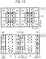
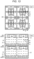
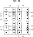
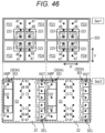
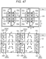
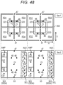
- Figs. 12 and 13 illustrate an example of the cross-sectional configuration in the horizontal direction of the image sensor 1.
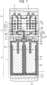
- the upper views of Figs. 12 and 13 illustrate an example of the cross-sectional configuration of a cross-section Sec1 of Fig. 7
- the lower views of Figs. 12 and 13 illustrate the cross-sectional configuration of a cross-section Sec2 of Fig. 7 .
- Fig. 12 illustrates a configuration in which two sets of two-by-two, four sensor pixels 12 are arranged in a second direction V2.
- Fig. 13 illustrates a configuration in which four sets of two-by-two four sensor pixels 12 are arranged in a first direction V1 and the second direction V2.
- a view illustrating an example of the front surface configuration of the semiconductor substrate 11 is superimposed on a view illustrating an example of the cross-sectional configuration of the cross-section Sec1 of Fig. 7 , but the insulating layer 240 is omitted.
- a view illustrating an example of the front surface configuration of the semiconductor substrate 303 is superimposed on a view illustrating an example of the cross-sectional configuration of the cross-section Sec2 of Fig. 7 .
- the first direction V1 is parallel to one arrangement direction (e.g., column direction) of the two arrangement directions (e.g., row direction and column direction) of the plurality of sensor pixels 12 arranged in a matrix.
- the four floating diffusion regions FDs are arranged close to each other, in one example, through the pixel separation portion 203.
- the gate electrodes 223 of the four transfer transistors TRs are arranged to surround the four floating diffusion regions FDs. In one example, the four gate electrodes 223 form a ring shape.
- the insulating layer 53 which exists in the portion of the semiconductor substrate 303 mentioned above through which the contact Ct penetrates, includes a plurality of blocks extending in the first direction V1.
- the semiconductor substrate 303 extends in the first direction V1 and includes a plurality of island-shaped blocks 303A arranged side by side in the second direction V2 orthogonal to the first direction V1 via the insulating layer 53 described above.
- Each block 303A is provided with, in one example, a plurality of sets of reset transistors RSTs, amplification transistors AMPs, and selection transistors SELs.
- One readout circuit 22 shared by four sensor pixels 12 includes, in one example, the reset transistor RST, the amplification transistor AMP, and the selection transistor SEL in a region facing four sensor pixels 12.
- One readout circuit 22 shared by four sensor pixels 12 includes, in one example, the amplification transistor AMP in the block 303A to the immediate left of the insulating layer 53, and includes the reset transistor RST and the selection transistor SEL in the block 303A to the immediate right of the insulating layer 53.
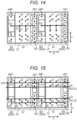
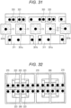
- the power supply line VDD is arranged, in one example, at a position facing each of the readout circuits 22 arranged side by side in the second direction V2, as illustrated in Fig. 15 .
- the power supply line VDD is electrically connected to the drain of the amplification transistor AMP and the drain of the reset transistor RST of each of the readout circuits 22 arranged side by side in the second direction V2 via the contact Ct2, in one example, as illustrated in Fig. 15 .
- the two pixel drive lines 23 are arranged, in one example, at a position facing each of the readout circuits 22 arranged side by side in the second direction V2, as illustrated in Fig. 15 .
- the vertical signal line 24 is arranged, in one example, at a position facing each readout circuit 22 arranged side by side in the first direction V1, as illustrated in Fig. 17 .
- the vertical signal line 24 (output line) is, in one example, electrically connected to the output terminal (source of the amplification transistor AMP) of each readout circuit 22 arranged side by side in the first direction V1, as illustrated in Fig. 17 .
- the semiconductor region and the pixel separation portion 203 are first formed in the first substrate 10 that is a silicon substrate, and the photodiode PD and the transfer transistor TR are provided for each pixel.
- the N-type drain region 221 and the N-type source region 222 are formed in the vicinity of the surface of the P-type semiconductor region (P-well) 204 partitioned by the pixel separation portion 203.
- the gate electrode 223 is formed between them. More specifically, an opening is defined between the N-type drain region 221 and the N-type source region 222 of the P-type semiconductor region 204. The opening leads to the photodiode PD (not illustrated in Fig.
- the gate electrode 223 is formed to fill the opening.
- the gate electrode 223 leads to a photodiode PD formed below the semiconductor region 204 (see Fig. 7 ).
- a region 205 illustrated in Fig. 7 indicates a region for one pixel partitioned by the pixel separation portion 203.
- an electrode 230 is formed on the P-type semiconductor region 204.
- the electrode 230 is used for leading the photodiode PD to the reference potential line to which the reference potential (e.g., ground) is supplied.
- the electrode 230 is provided for each pixel and leads to the photodiode PD (not illustrated).
- the transfer transistor TR is an N-channel type MOS transistor, and its drain region 221 is an N-type semiconductor region.
- the drain region 221 of the transfer transistor TR leads to the P-type semiconductor region 202 that covers the side surface of the photodiode PD.
- the terminal, which is not connected to the transfer transistor TR (input side terminal), of two terminals of the photodiode PD leads to the reference potential line.
- the photodiode PD is connected to the reference potential line via the electrode 230.
- the electrode 230 connected to the photodiode PD formed in the N-type semiconductor region is formed as P-type polysilicon.
- the N-type drain region 221, the N-type source region 222, the gate electrodes 223, and the electrode 230 are provided for each pixel in the P-type semiconductor region 204, and then they are covered with the insulating layer 240.
- the insulating layer 240 is configured as an oxide film such as SiO 2 .
- the insulating layer 240 is etched to form a wiring groove 241 and a wiring groove 242.
- the wiring groove 241 is used to form a wiring 301a that aggregates the source regions 222 of the plurality of transfer transistors TRs.
- the wiring groove 242 is used to form a wiring 301b that aggregates the plurality of electrodes 230.
- the wiring 301a and the wiring 301b are often referred herein to as simply "wiring 301" unless they are necessary to be distinguished.
- the source region 222 of the transfer transistor TR is an N-type semiconductor region, so the wiring 301a connected to the source region 222 is formed as P-type polysilicon.
- the electrode 230 is P-type polysilicon, so the wiring 301b connected to the electrode 230 is formed as N-type polysilicon.
- the wiring 301a that aggregates the output terminal sides of the plurality of transfer transistors TR is formed as P-type polysilicon.
- the electrode 230 connected to the photodiode PD formed in the N-type semiconductor region is formed as P-type polysilicon.
- the wiring 301b that aggregates the plurality of electrodes 230 is formed as N-type polysilicon.
- the P-type polysilicon which is a material for the wiring 301a
- the N-type polysilicon which is a material for the wiring 301b
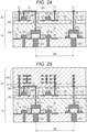
- the resultant deposit is polished using chemical mechanical polishing (CMP) to form the wiring 301a and the wiring 301b (see Fig. 20 ).
- the wiring 301a is connected to the source regions 222 of four transfer transistors TRs having a one-to-one correspondence with the four photodiodes PDs.
- the wiring 301a aggregates the source regions 222 of the four transfer transistors TRs having a one-to-one correspondence with the four photodiodes PDs for each of the four photodiodes PDs.
- the wiring 301a is connected to the wiring D1 via one contact Ct to connect the aggregated source region 222 to the wiring D1 of the second substrate 20 leading to the gate electrode 311 of the amplification transistor AMP shared by the source regions 222.
- one contact Ct is provided for every four source regions 222.
- the source regions 222 of the transfer transistor TR corresponds to the "first element”
- the gate electrode 311 of the amplification transistor AMP corresponds to the "second element”.
- the wiring D1 corresponds to the "first wiring” or the “second wiring formed on the second substrate”
- the wiring 301a corresponds to the "second wiring” or the "first wiring formed on the first substrate and connected to the first photoelectric transducer and the second photoelectric transducer".
- the number of pixels as a constituent unit for aggregation by the wiring 301a is not limited to four and can be optional.
- the wiring 301b is connected to four electrodes 230 having a one-to-one correspondence with the four photodiodes PDs.
- the wiring 301b aggregates four electrodes 230 having a one-to-one correspondence with the four photodiodes PDs.
- the wiring 301b is connected to the wiring D1 via one contact Ct to connect the aggregated electrodes 230 to the wiring D1 of the second substrate 20 leading to the reference potential line shared by the electrodes 230.
- one contact Ct is provided for every four electrodes 230.
- the wiring D1 leading to the reference potential line is different from the wiring D1 leading to the gate electrode 311 of the amplification transistor AMP described above (however, both are wirings formed on the insulating layer 245 of the second substrate 20).
- the electrode 230 corresponds to the "first element”
- the reference potential line corresponds to the "second element”.
- the wiring D1 corresponds to the "first wiring”
- the wiring 301b corresponds to the "second wiring”.
- the number of pixels as a constituent unit for aggregation by the wiring 301b is not limited to four and can be optional.
- the wirings 301b are connected (indirectly connected) to the respective corresponding photodiodes PDs via each electrode 230.
- the wiring 301b also corresponds to the "first wiring formed on the first substrate and connected to the first photoelectric transducer and the second photoelectric transducer".
- the wiring D1 also corresponds to the "second wiring formed on the second substrate”.
- the reference potential line is formed on the second substrate 20, but its configuration is not limited to the example above, and the reference potential line can be formed on, in one example, another substrate (such as the third substrate 30).
- the "second element" is not limited to an element formed on the second substrate 20.
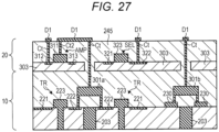
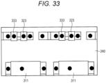
- the insulating layer 240 is deposited on the wiring 301a and the wiring 301b. Then, the P-type semiconductor substrate 303 is joined on top of the insulating layer 240 and is thinned.
- a portion of the semiconductor substrate 303 that faces the wiring 301 is opened to form a pixel transistor on the semiconductor substrate 303.
- the amplification transistor AMP and the selection transistor SEL are illustrated, but the reset transistor RST (not illustrated) is also formed on the semiconductor substrate 303.
- an N-type drain region 312 and an N-type source region 313 are formed in the vicinity of the surface of the semiconductor substrate 303.
- the gate electrode 311 is formed between them to form the amplification transistor AMP.
- an N-type drain region 321 and an N-type source region 322 are formed in the vicinity of the surface of the semiconductor substrate 303, a gate electrode 323 is formed between them to form the selection transistor SEL.
- the reset transistor RST (not illustrated) is also formed in a similar manner.
- the insulating layer 245 is formed (deposited) so that it covers the opening and the pixel transistor (such as amplification transistor AMP and selection transistor SEL) formed as described above.
- the contacts Ct and Ct2 are formed for connecting the wiring 301 and each element of the second substrate 20 to the wiring D1.
- the contact Ct is provided for each of the drain region 312 of the amplification transistor AMP, the wiring 301, and the source region 322 of the selection transistor SEL.
- the contact Ct2 is provided for the gate electrode 311 of the amplification transistor AMP.
- a way is considered of etching the insulating layer to form an opening defining the contacts Ct and Ct2, forming a barrier layer for electrically insulating on the inner surface of the opening, then filling it with a material of the contacts Ct and Ct2.
- the insulating layer (the insulating layer covering the side surface of the contact Ct) provided at the opening of the semiconductor substrate 303 is the insulating layer 53 described above.
- Examples of the material of the contacts Ct and Ct2 include tungsten or the like.
- the barrier layer includes, in one example, Ti, TiN, Ta, TaN, or the like as material.
- the method of forming the contacts Ct and Ct2 and their materials are not limited to the example above and are optional, and various known techniques can be employed.
- the wiring layer 246 described above is formed on the insulating layer 245.
- the third substrate 30 on which the peripheral circuit is formed is joined to form a color filter and an on-chip lens for each pixel.
- the configuration illustrated in Fig. 7 can be obtained.
- a region 270 indicates a set of connection points 271 between the electrodes 230 and the wiring 301b for each of the four electrodes 230 having a one-to-one correspondence with four photodiodes PDs as a constituent unit of sharing the reference potential line.
- first substrate 10 and the second substrate 20 separated from each other make it possible to increase the number of pixels per unit area, as compared with the configuration in which the photodiode PD and the pixel transistor are provided on the same substrate, improving the resolution.
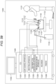
- the lens unit 11401 is an optical system, provided at a connecting location to the lens barrel 11101. Observation light taken in from a distal end of the lens barrel 11101 is guided to the camera head 11102 and introduced into the lens unit 11401.
- the lens unit 11401 includes a combination of a plurality of lenses including a zoom lens and a focusing lens.
- the communication unit 11404 includes a communication apparatus for transmitting and receiving various kinds of information to and from the CCU 11201.
- the communication unit 11404 transmits an image signal acquired from the imaging unit 11402 as RAW data to the CCU 11201 through the transmission cable 11400.
- the communication unit 11411 transmits a control signal for controlling driving of the camera head 11102 to the camera head 11102.
- the image signal and the control signal can be transmitted by electrical communication, optical communication or the like.
- the description above is given of an example of the endoscopic surgery system to which the technology according to the present disclosure is applicable.
- the technology according to the present disclosure is suitably applicable to the imaging unit 11402 provided on the camera head 11102 of the endoscope 11100 in the configuration described above.
- the technology according to the present disclosure applied to the imaging unit 11402 makes it possible to reduce the size of the imaging unit 11402 or achieve high-definition image capturing unit. Thus, it is possible to provide a small-sized or high-definition endoscope 11100.
- present technology may also be configured as below.
Landscapes
- Engineering & Computer Science (AREA)
- Multimedia (AREA)
- Signal Processing (AREA)
- Solid State Image Pick-Up Elements (AREA)
- Transforming Light Signals Into Electric Signals (AREA)
- Internal Circuitry In Semiconductor Integrated Circuit Devices (AREA)
- Metal-Oxide And Bipolar Metal-Oxide Semiconductor Integrated Circuits (AREA)
Applications Claiming Priority (3)
| Application Number | Priority Date | Filing Date | Title |
|---|---|---|---|
| JP2018195638 | 2018-10-17 | ||
| EP19874154.8A EP3869563B1 (de) | 2018-10-17 | 2019-10-15 | Bildgebungselement und elektronische ausrüstung |
| PCT/JP2019/040372 WO2020080327A1 (ja) | 2018-10-17 | 2019-10-15 | 撮像素子および電子機器 |
Related Parent Applications (1)
| Application Number | Title | Priority Date | Filing Date |
|---|---|---|---|
| EP19874154.8A Division EP3869563B1 (de) | 2018-10-17 | 2019-10-15 | Bildgebungselement und elektronische ausrüstung |
Publications (2)
| Publication Number | Publication Date |
|---|---|
| EP4580349A2 true EP4580349A2 (de) | 2025-07-02 |
| EP4580349A3 EP4580349A3 (de) | 2025-10-01 |
Family
ID=70283447
Family Applications (2)
| Application Number | Title | Priority Date | Filing Date |
|---|---|---|---|
| EP19874154.8A Active EP3869563B1 (de) | 2018-10-17 | 2019-10-15 | Bildgebungselement und elektronische ausrüstung |
| EP25173359.8A Pending EP4580349A3 (de) | 2018-10-17 | 2019-10-15 | Bildsensor und elektronische vorrichtung |
Family Applications Before (1)
| Application Number | Title | Priority Date | Filing Date |
|---|---|---|---|
| EP19874154.8A Active EP3869563B1 (de) | 2018-10-17 | 2019-10-15 | Bildgebungselement und elektronische ausrüstung |
Country Status (7)
| Country | Link |
|---|---|
| US (3) | US12148787B2 (de) |
| EP (2) | EP3869563B1 (de) |
| JP (2) | JP7472032B2 (de) |
| KR (2) | KR102855026B1 (de) |
| CN (2) | CN119967917A (de) |
| TW (3) | TWI887068B (de) |
| WO (1) | WO2020080327A1 (de) |
Families Citing this family (11)
| Publication number | Priority date | Publication date | Assignee | Title |
|---|---|---|---|---|
| JP7695932B2 (ja) * | 2020-05-29 | 2025-06-19 | ソニーセミコンダクタソリューションズ株式会社 | 半導体装置及び電子機器 |
| JP2022049487A (ja) | 2020-09-16 | 2022-03-29 | ソニーグループ株式会社 | 固体撮像装置及び電子機器 |
| JP2022092536A (ja) * | 2020-12-10 | 2022-06-22 | ソニーセミコンダクタソリューションズ株式会社 | 撮像素子及び撮像装置 |
| KR102940126B1 (ko) | 2021-03-16 | 2026-03-16 | 삼성전자주식회사 | 이미지 센서 |
| KR20220149243A (ko) * | 2021-04-30 | 2022-11-08 | 에스케이하이닉스 주식회사 | 이미지 센싱 장치 |
| JP2024004794A (ja) * | 2022-06-29 | 2024-01-17 | キヤノン株式会社 | 光電変換装置、機器、積層体 |
| US20240021641A1 (en) * | 2022-07-14 | 2024-01-18 | Taiwan Semiconductor Manufacturing Company, Ltd. | Dielectric structure for small pixel designs |
| CN119498035A (zh) * | 2022-07-26 | 2025-02-21 | 索尼半导体解决方案公司 | 固态成像装置及其制造方法 |
| JP2024112734A (ja) * | 2023-02-08 | 2024-08-21 | ソニーセミコンダクタソリューションズ株式会社 | 光検出装置および電子機器 |
| WO2025094686A1 (ja) * | 2023-11-02 | 2025-05-08 | ソニーセミコンダクタソリューションズ株式会社 | 光検出装置、および撮像装置、並びに電子機器 |
| JP2025089933A (ja) * | 2023-12-04 | 2025-06-16 | キヤノン株式会社 | 半導体装置、半導体装置の製造方法、光電変換システムおよび移動体 |
Citations (1)
| Publication number | Priority date | Publication date | Assignee | Title |
|---|---|---|---|---|
| JP2010245506A (ja) | 2009-03-19 | 2010-10-28 | Sony Corp | 半導体装置とその製造方法、及び電子機器 |
Family Cites Families (25)
| Publication number | Priority date | Publication date | Assignee | Title |
|---|---|---|---|---|
| US8049293B2 (en) * | 2005-03-07 | 2011-11-01 | Sony Corporation | Solid-state image pickup device, electronic apparatus using such solid-state image pickup device and method of manufacturing solid-state image pickup device |
| KR100782463B1 (ko) | 2005-04-13 | 2007-12-05 | (주)실리콘화일 | 3차원 구조를 갖는 이미지 센서의 분리형 단위화소 및 그제조방법 |
| JP2007228460A (ja) * | 2006-02-27 | 2007-09-06 | Mitsumasa Koyanagi | 集積センサを搭載した積層型半導体装置 |
| EP2158607A1 (de) * | 2007-06-19 | 2010-03-03 | SiliconFile Technologies Inc. | Pixelanordnung zur vermeidung von übersprechung zwischen pixeln einer einheit und bildsensor mit dem pixel |
| KR101648200B1 (ko) | 2009-10-22 | 2016-08-12 | 삼성전자주식회사 | 이미지 센서 및 그 제조 방법 |
| JP5479179B2 (ja) * | 2009-11-30 | 2014-04-23 | 富士フイルム株式会社 | 液晶表示装置 |
| JP5489705B2 (ja) * | 2009-12-26 | 2014-05-14 | キヤノン株式会社 | 固体撮像装置および撮像システム |
| JP2012033894A (ja) * | 2010-06-30 | 2012-02-16 | Canon Inc | 固体撮像装置 |
| JP5500007B2 (ja) * | 2010-09-03 | 2014-05-21 | ソニー株式会社 | 固体撮像素子およびカメラシステム |
| JP6402624B2 (ja) | 2012-03-30 | 2018-10-10 | 株式会社ニコン | 撮像素子および撮像装置 |
| JP2014022561A (ja) * | 2012-07-18 | 2014-02-03 | Sony Corp | 固体撮像装置、及び、電子機器 |
| KR101402750B1 (ko) | 2012-09-26 | 2014-06-11 | (주)실리콘화일 | 3차원 구조를 가지는 이미지센서의 분리형 단위화소 |
| KR101334213B1 (ko) * | 2013-09-02 | 2013-11-29 | (주)실리콘화일 | 칩 적층 이미지 센서 |
| JP6334203B2 (ja) * | 2014-02-28 | 2018-05-30 | ソニー株式会社 | 固体撮像装置、および電子機器 |
| US9774801B2 (en) * | 2014-12-05 | 2017-09-26 | Qualcomm Incorporated | Solid state image sensor with enhanced charge capacity and dynamic range |
| TWI692859B (zh) | 2015-05-15 | 2020-05-01 | 日商新力股份有限公司 | 固體攝像裝置及其製造方法、以及電子機器 |
| US10014333B2 (en) * | 2015-08-26 | 2018-07-03 | Semiconductor Components Industries, Llc | Back-side illuminated pixels with interconnect layers |
| JP6808348B2 (ja) * | 2016-04-28 | 2021-01-06 | キヤノン株式会社 | 光電変換装置およびカメラ |
| JP6661506B2 (ja) * | 2016-09-23 | 2020-03-11 | サムスン エレクトロニクス カンパニー リミテッド | 固体撮像装置 |
| CN117558738A (zh) | 2017-04-04 | 2024-02-13 | 索尼半导体解决方案公司 | 固态摄像装置和电子设备 |
| WO2018207345A1 (ja) * | 2017-05-12 | 2018-11-15 | オリンパス株式会社 | 固体撮像装置 |
| JP7038494B2 (ja) * | 2017-06-15 | 2022-03-18 | ルネサスエレクトロニクス株式会社 | 固体撮像素子 |
| KR102430496B1 (ko) * | 2017-09-29 | 2022-08-08 | 삼성전자주식회사 | 이미지 센싱 장치 및 그 제조 방법 |
| KR102483548B1 (ko) * | 2017-10-31 | 2023-01-02 | 삼성전자주식회사 | 이미지 센싱 장치 |
| KR102646903B1 (ko) * | 2018-09-04 | 2024-03-12 | 삼성전자주식회사 | 이미지 센서 |
-
2019
- 2019-10-14 TW TW113128732A patent/TWI887068B/zh active
- 2019-10-14 TW TW113108656A patent/TWI886830B/zh active
- 2019-10-14 TW TW108136925A patent/TWI848008B/zh active
- 2019-10-15 CN CN202510082758.2A patent/CN119967917A/zh active Pending
- 2019-10-15 EP EP19874154.8A patent/EP3869563B1/de active Active
- 2019-10-15 CN CN201980059496.0A patent/CN112689900B/zh active Active
- 2019-10-15 KR KR1020247034625A patent/KR102855026B1/ko active Active
- 2019-10-15 KR KR1020217008366A patent/KR102720386B1/ko active Active
- 2019-10-15 EP EP25173359.8A patent/EP4580349A3/de active Pending
- 2019-10-15 JP JP2020553169A patent/JP7472032B2/ja active Active
- 2019-10-15 US US17/284,699 patent/US12148787B2/en active Active
- 2019-10-15 WO PCT/JP2019/040372 patent/WO2020080327A1/ja not_active Ceased
-
2024
- 2024-04-09 JP JP2024062766A patent/JP7732022B2/ja active Active
- 2024-04-11 US US18/633,060 patent/US12615872B2/en active Active
- 2024-10-08 US US18/909,452 patent/US20250040287A1/en active Pending
Patent Citations (1)
| Publication number | Priority date | Publication date | Assignee | Title |
|---|---|---|---|---|
| JP2010245506A (ja) | 2009-03-19 | 2010-10-28 | Sony Corp | 半導体装置とその製造方法、及び電子機器 |
Also Published As
| Publication number | Publication date |
|---|---|
| JP2024086835A (ja) | 2024-06-28 |
| EP3869563A1 (de) | 2021-08-25 |
| KR20210075075A (ko) | 2021-06-22 |
| EP4580349A3 (de) | 2025-10-01 |
| TWI848008B (zh) | 2024-07-11 |
| WO2020080327A1 (ja) | 2020-04-23 |
| EP3869563A4 (de) | 2022-01-26 |
| US20250040287A1 (en) | 2025-01-30 |
| TW202429702A (zh) | 2024-07-16 |
| JPWO2020080327A1 (ja) | 2021-09-16 |
| JP7732022B2 (ja) | 2025-09-01 |
| TWI886830B (zh) | 2025-06-11 |
| CN112689900B (zh) | 2025-01-21 |
| TW202445853A (zh) | 2024-11-16 |
| KR20240155373A (ko) | 2024-10-28 |
| US20240258358A1 (en) | 2024-08-01 |
| CN119967917A (zh) | 2025-05-09 |
| US12148787B2 (en) | 2024-11-19 |
| KR102720386B1 (ko) | 2024-10-23 |
| KR102855026B1 (ko) | 2025-09-04 |
| CN112689900A (zh) | 2021-04-20 |
| JP7472032B2 (ja) | 2024-04-22 |
| EP3869563B1 (de) | 2025-05-07 |
| TW202029487A (zh) | 2020-08-01 |
| US12615872B2 (en) | 2026-04-28 |
| TWI887068B (zh) | 2025-06-11 |
| US20210343776A1 (en) | 2021-11-04 |
Similar Documents
| Publication | Publication Date | Title |
|---|---|---|
| US12266675B2 (en) | Imaging element | |
| US12615872B2 (en) | Image sensor and electronic apparatus | |
| JP7541971B2 (ja) | 撮像装置 | |
| US12262129B2 (en) | Solid-state imaging device and electronic apparatus including two floating diffusion regions | |
| US12119359B2 (en) | Imaging device | |
| US20220384207A1 (en) | Imaging device and method of manufacturing imaging device | |
| US20220157876A1 (en) | Imaging unit, method of manufacturing imaging unit, and semiconductor device | |
| US20240250106A1 (en) | Image sensor | |
| US12501733B2 (en) | Semiconductor device and imaging unit | |
| US20250072150A1 (en) | Imaging element and method of manufacturing imaging element | |
| US12514017B2 (en) | Wiring structure, method of manufacturing the same, and imaging device | |
| US20230275020A1 (en) | Wiring structure, method of manufacturing the same, and imaging device |
Legal Events
| Date | Code | Title | Description |
|---|---|---|---|
| PUAI | Public reference made under article 153(3) epc to a published international application that has entered the european phase |
Free format text: ORIGINAL CODE: 0009012 |
|
| STAA | Information on the status of an ep patent application or granted ep patent |
Free format text: STATUS: REQUEST FOR EXAMINATION WAS MADE |
|
| 17P | Request for examination filed |
Effective date: 20250429 |
|
| AC | Divisional application: reference to earlier application |
Ref document number: 3869563 Country of ref document: EP Kind code of ref document: P |
|
| AK | Designated contracting states |
Kind code of ref document: A2 Designated state(s): AL AT BE BG CH CY CZ DE DK EE ES FI FR GB GR HR HU IE IS IT LI LT LU LV MC MK MT NL NO PL PT RO RS SE SI SK SM TR |
|
| REG | Reference to a national code |
Ref country code: DE Ref legal event code: R079 Free format text: PREVIOUS MAIN CLASS: H10F0039180000 Ipc: H10F0039000000 |
|
| PUAL | Search report despatched |
Free format text: ORIGINAL CODE: 0009013 |
|
| AK | Designated contracting states |
Kind code of ref document: A3 Designated state(s): AL AT BE BG CH CY CZ DE DK EE ES FI FR GB GR HR HU IE IS IT LI LT LU LV MC MK MT NL NO PL PT RO RS SE SI SK SM TR |
|
| RIC1 | Information provided on ipc code assigned before grant |
Ipc: H10F 39/00 20250101AFI20250827BHEP Ipc: H04N 25/778 20230101ALI20250827BHEP Ipc: H04N 25/79 20230101ALI20250827BHEP Ipc: H04N 25/76 20230101ALI20250827BHEP |