EP4530722A2 - Schaltbare unterschichten für die euv-lithographie - Google Patents
Schaltbare unterschichten für die euv-lithographie Download PDFInfo
- Publication number
- EP4530722A2 EP4530722A2 EP24195966.7A EP24195966A EP4530722A2 EP 4530722 A2 EP4530722 A2 EP 4530722A2 EP 24195966 A EP24195966 A EP 24195966A EP 4530722 A2 EP4530722 A2 EP 4530722A2
- Authority
- EP
- European Patent Office
- Prior art keywords
- car
- sul
- component
- grafting
- resist
- Prior art date
- Legal status (The legal status is an assumption and is not a legal conclusion. Google has not performed a legal analysis and makes no representation as to the accuracy of the status listed.)
- Pending
Links
Images


Classifications
-
- G—PHYSICS
- G03—PHOTOGRAPHY; CINEMATOGRAPHY; ANALOGOUS TECHNIQUES USING WAVES OTHER THAN OPTICAL WAVES; ELECTROGRAPHY; HOLOGRAPHY
- G03F—PHOTOMECHANICAL PRODUCTION OF TEXTURED OR PATTERNED SURFACES, e.g. FOR PRINTING, FOR PROCESSING OF SEMICONDUCTOR DEVICES; MATERIALS THEREFOR; ORIGINALS THEREFOR; APPARATUS SPECIALLY ADAPTED THEREFOR
- G03F7/00—Photomechanical, e.g. photolithographic, production of textured or patterned surfaces, e.g. printing surfaces; Materials therefor, e.g. comprising photoresists; Apparatus specially adapted therefor
- G03F7/004—Photosensitive materials
- G03F7/09—Photosensitive materials characterised by structural details, e.g. supports, auxiliary layers
- G03F7/11—Photosensitive materials characterised by structural details, e.g. supports, auxiliary layers having cover layers or intermediate layers, e.g. subbing layers
-
- G—PHYSICS
- G03—PHOTOGRAPHY; CINEMATOGRAPHY; ANALOGOUS TECHNIQUES USING WAVES OTHER THAN OPTICAL WAVES; ELECTROGRAPHY; HOLOGRAPHY
- G03F—PHOTOMECHANICAL PRODUCTION OF TEXTURED OR PATTERNED SURFACES, e.g. FOR PRINTING, FOR PROCESSING OF SEMICONDUCTOR DEVICES; MATERIALS THEREFOR; ORIGINALS THEREFOR; APPARATUS SPECIALLY ADAPTED THEREFOR
- G03F7/00—Photomechanical, e.g. photolithographic, production of textured or patterned surfaces, e.g. printing surfaces; Materials therefor, e.g. comprising photoresists; Apparatus specially adapted therefor
- G03F7/004—Photosensitive materials
- G03F7/075—Silicon-containing compounds
- G03F7/0752—Silicon-containing compounds in non photosensitive layers or as additives, e.g. for dry lithography
-
- G—PHYSICS
- G03—PHOTOGRAPHY; CINEMATOGRAPHY; ANALOGOUS TECHNIQUES USING WAVES OTHER THAN OPTICAL WAVES; ELECTROGRAPHY; HOLOGRAPHY
- G03F—PHOTOMECHANICAL PRODUCTION OF TEXTURED OR PATTERNED SURFACES, e.g. FOR PRINTING, FOR PROCESSING OF SEMICONDUCTOR DEVICES; MATERIALS THEREFOR; ORIGINALS THEREFOR; APPARATUS SPECIALLY ADAPTED THEREFOR
- G03F7/00—Photomechanical, e.g. photolithographic, production of textured or patterned surfaces, e.g. printing surfaces; Materials therefor, e.g. comprising photoresists; Apparatus specially adapted therefor
- G03F7/20—Exposure; Apparatus therefor
- G03F7/2002—Exposure; Apparatus therefor with visible light or UV light, through an original having an opaque pattern on a transparent support, e.g. film printing, projection printing; by reflection of visible or UV light from an original such as a printed image
- G03F7/2004—Exposure; Apparatus therefor with visible light or UV light, through an original having an opaque pattern on a transparent support, e.g. film printing, projection printing; by reflection of visible or UV light from an original such as a printed image characterised by the use of a particular light source, e.g. fluorescent lamps or deep UV light
-
- G—PHYSICS
- G03—PHOTOGRAPHY; CINEMATOGRAPHY; ANALOGOUS TECHNIQUES USING WAVES OTHER THAN OPTICAL WAVES; ELECTROGRAPHY; HOLOGRAPHY
- G03F—PHOTOMECHANICAL PRODUCTION OF TEXTURED OR PATTERNED SURFACES, e.g. FOR PRINTING, FOR PROCESSING OF SEMICONDUCTOR DEVICES; MATERIALS THEREFOR; ORIGINALS THEREFOR; APPARATUS SPECIALLY ADAPTED THEREFOR
- G03F7/00—Photomechanical, e.g. photolithographic, production of textured or patterned surfaces, e.g. printing surfaces; Materials therefor, e.g. comprising photoresists; Apparatus specially adapted therefor
- G03F7/26—Processing photosensitive materials; Apparatus therefor
- G03F7/38—Treatment before imagewise removal, e.g. prebaking
Definitions
- the present disclosure generally relates to semiconductor lithography and more particularly to structures including or formed using a photoresist underlayer and to methods of forming such structures.
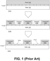
- Fig. 1 is a diagram schematically illustrating a portion of a conventional lithographic manufacturing process for a semiconductor device.
- fine patterns of features can be formed on a surface of a substrate 105 by patterning the surface of the substrate and etching material from the substrate surface using, for example, gas-phase etching processes.
- gas-phase etching processes As a density of devices on a substrate increases, it becomes increasingly desirable to form features with smaller dimensions.
- a photoresist (resist) layer 120 is used to pattern a surface of a substrate prior to etching.
- the resist layer 120 is applied to a surface of the substrate 105, usually on top of an underlayer material 110, which among other things, serves as an adhesive to adhere the photoresist to the substrate surface.
- the photoresist is then exposed to radiation from a mask having a desired feature pattern.
- Techniques have recently been developed to use extreme ultraviolet (EUV) wavelengths to develop patterns having relatively small pattern features (e.g., 10 nm or less).
- EUV extreme ultraviolet
- the radiation (EUV) pattern is projected onto the resist, exposing the pattern, or non-pattern, portions, depending on whether a positive or negative resist material is used. From here, either the exposed (positive) or non-exposed (negative) portions are removed using a developer. This is represented at 101B. With this example, a positive resist is used where the exposed portions are removed. Thus, as shown at 101C, the exposed resist portions 120B are removed. This is referred to as the development step.
- EUV photoresists Most of the EUV photoresists (resists) used today are chemically amplified resists (CARs). In contrast with other photoresist materials, within a CAR incoming light does not directly cause the backbone polymer to become soluble. Rather, the light is absorbed by photoacid generators (PAGs), which release multiple photoacid molecules per photon. The photoacid reacts with protective groups on the polymer backbone, "de-protecting" it and causing it to become soluble in developer solution (e.g., aqueous development solution). With EUV resists, the incoming light can also excite photoelectrons, which in turn can also drive the photoacid generation reaction.
- CARs chemically amplified resists
- CARs chemically amplified resists
- ⁇ scum' unwanted material within the exposed region
- the plasma also detrimentally eats away at the unexposed photoresist.
- the underlayer should provide good photoresist adhesion in order to achieve satisfactory lithographic feature definition and sufficient process windows for good patterning, but increased resist-underlayer adhesion also gives rise to an increase in resist scum remaining.
- a switchable underlayer (SUL) is provided that gives strong resist adhesion to promote patterning performance but also can utilize the built-in photoacid generation from CARs (chemically amplified resists) to promote an adhesion switch at the resist/underlayer interface.
- the SUL has molecules that switch from being resist-philic to resist-phobic upon EUV exposure, producing an underlayer that facilitates more effective development and scum removal, requiring less aggressive de-scumming.
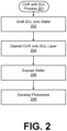
- FIG. 2 is a flow diagram showing a part of a lithographic process using a CAR with a SUL in accordance with some embodiments.
- Fig. 3A is a diagram schematically illustrating wafer stages using the process of Fig. 2 in accordance with some embodiments.
- Fig. 3B is a schematic view of the wafer of Fig. 3A , illustrating a SUL grafting and switchable adhesion structure, in accordance with some embodiments.
- a thin SUL layer (e.g., a mono-molecular layer) 310 is grafted onto the surface of a wafer 305.
- the SUL may be grafted to the wafer surface using any suitable approach. For example, it may be done with several different techniques. It could be applied using a spin-coating method, e.g., in a similar fashion to how the CAR (hereinafter referred to as CAR or resist) is deposited. However, this approach may not be ideal because, for example, vapor from the SUL can leave deposits causing issues for subsequent coating applications and may not provide desired adhesion of the resist.
- VPD vapor phase deposition
- Fig. 3B illustrates a structure for grafting (or anchoring) the SUL onto the wafer surface in accordance with some embodiments.
- the approach, and chemical grafting mechanism will depend on the make-up of the actual surface to which the SUL is being applied.
- the wafer surface 307 is formed from an oxide or nitride such as silicon oxide or silicon nitride, which, for example, as a result of the surface hydroxyl groups, will exhibit a poor affinity for the non-polar or low-polar molecules of the resist. Therefore, the SUL needs a way to form an adhesive bridge between the polar wafer surface and non-polar resist material.
- the SUL may be formed from a SUL molecule having, among other things, a grafting component, and an adhesive component.
- a SUL molecule having, among other things, a grafting component, and an adhesive component.
- the SUL 310 including a Si-O grafting component 312 and a SUL adhesive (SULA) component 314.
- the Si-O grafting component 312 anchors itself to the wafer's Si-O2 surface, forming strong bonds with the embedded hydroxyl groups.
- the SULA component 314 provides non-polar head groups that can be adhered to by the resist 320.
- the SULA head groups display strong adhesive forces for the resist, improving patterning and preventing line collapse.
- the CAR is applied atop the SUL.
- the CAR may be deposited using any suitable method such as spin coating or vapor phase deposition.
- the CAR 320 has been applied, and the wafer is ready for exposure.
- the resist is illuminated (exposed), e.g., from EUV radiation projected off of an EUV mask. It then goes through a post exposure bake (PEB) stage, e.g., 120 degrees C for 1 minute.
- PEB post exposure bake
- the PEB energizes the photoacids created from the EUV photons and breaks down the exposed CAR structure (polymer deprotection).
- the energized CAR photoacids also switch the SUL molecules under the exposed CAR portions (e.g., cleave away the adhesive components from the SUL molecules) to produce the lower adhesivity state of the SUL.
- the head groups within the exposed SUL regions undergo switching to reveal resist-phobic functional groups ('mis-matched' interface), which aids in the full removal of resist and decreases scumming.
- the switching reactions are piggy-backed off of the photoacids that are already being created by the CAR during exposure.
- the adhesive components could be removed by reactants (e.g., acids) generated within the SUL material itself from impinging photons and/or by-product electrons during exposure.
- reactants e.g., acids
- active photoacid generating components used by the CAR could be incorporated into the SUL material itself.
- the exposed and baked wafer is depicted at 301B.
- the SUL portions beneath the unexposed CAR portions 320A are unaffected, not "switched" as indicated by darker shading.
- the resist is developed.
- the structural polymer breakdown of the exposed CAR portions allows them to be soluble in a wash solution, e.g., an aqueous wash solution that can remove the exposed CAR material, as is indicated at 301C.
- a wash solution e.g., an aqueous wash solution that can remove the exposed CAR material
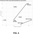
- Figure 4 is a diagram showing surface energy analysis of a SUL pre and post EUV processing as compared with other common UL materials (SiC, SiOx, spin-on-glass (SOG)).
- SiC SiC, SiOx, spin-on-glass
- SOG spin-on-glass
- the SUL material displayed a dispersive component value of 30 mN/M and a polar component value of 6 mN/M, similar to the CAR's properties (indicated at 'A'), which produces strong adhesive forces improving patterning and preventing line collapse.
- the SUL surface energy dramatically shifted with a dispersive component value of 38 mN/M and a polar component value of 25 mN/M, far away from the CAR, lowering the adhesive forces and making removal by the developer more energetically favorable.
- Work of adhesion analysis of SUL materials has demonstrated a 53% drop in adhesion from pre to post exposure/bake.
- Fig. 5 is a diagram showing exemplary SUL molecule structures in accordance with some embodiments.
- a SUL molecule may include a grafting group component (a), a resist adhesion component (b), a PEB activation-temperature control component (c), and a scum elimination control component (d).
- the grafting component (a) should be able to graft (or anchor) the molecule to the wafer surface being processed.
- a grafting group could include but is not limited to: silyl amides, silyl chlorides, trialkoxy silanes, phosphonates and alcohols.
- component groups used for a resist adhesion component could include but are not limited to: alkanes, pefluoroalkanes, aryl groups, polygylcols and polymers.
- the PEB activation-temperature control component should be selected to cause or allow the adhesion component to be cleaved from the SUL molecule within a range encompassing the utilized PEB temperature.
- the activation-temperature component might facilitate switching (e.g., deprotecting and cleaving of adhesion component) at a temperature of 120 degrees C, as well as at a temperature in a range of between 115 and 125 degrees C.
- the activation temperature should accommodate the temperature selected based on the utilized CAR.
- a component used for PEB activation temperature may be chosen from a group including but not limited to: aryl and heteroaryl rings substituted with electron donating substituents (e.g., methoxy, amino) or electron withdrawing substituents such as fluorine and nitro groups.
- electron donating substituents e.g., methoxy, amino
- electron withdrawing substituents such as fluorine and nitro groups.
- a scum elimination component should remain after exposure/PEB and should have sufficiently low adhesion with the utilized CAR material.
- a scum elimination component could be selected from a group including but not limited to carboxylates, amides, alcohols, thiols, amines and polymers.
- SUL SUL
- WCA water contact angles
- tert-butyl esters which switch from hydrophobic to hydrophilic upon deprotection with acid and heat.
- the wafer was then rinsed with fresh PGMEA to remove any unreacted byproducts.
- Successful formation of the SUL was confirmed by ellipsometry and water contact angle (WCA) measurement.
- WCA water contact angle
- a prototypical CAR containing polytertbutylmethacrylate-parahydroxystyrene copolymers, triphenyl sulfonium perfluoro-1-butanesufonate (photoacid generator) and trioctylamine (quencher) was deposited onto this SUL.
- Example 1 is a method of forming a structure comprising a photoresist underlayer.
- the method includes: (1) providing a substrate, (2) grafting a chemically amplified resist (CAR) switchable underlayer (SUL) to a surface of the substrate, the SUL having SUL molecules each with a grafting component to graft the SUL molecule to the substrate surface, (3) depositing a CAR layer onto the SUL, wherein the SUL molecules each have a resist adhesion component that adheres with the CAR, (4) performing an EUV scan operation on the CAR, wherein portions of the CAR are exposed to EUV radiation, and (5) performing a post-exposure bake (PEB) operation to the SUL and CAR, wherein the resist adhesion components are switched to being inactive, making the CAR less adhesive with the SUL.
- CAR chemically amplified resist
- SUL chemically amplified resist
- SUL chemically amplified resist
- SUL chemically amplified resist
- SUL chemical
- Example 2 includes the subject matter of example 1, and further comprising developing the CAR by washing away the exposed CAR residing over the switched SUL.
- Example 3 includes the subject matter of any of examples 1 and 2, and wherein the substrate surface is a silicon oxide surface.
- Example 4 includes the subject matter of any of examples 1-3, and wherein the grafting component is selected from a group consisting of silyl amides, silyl chlorides, trialkoxy silanes, phosphonates and alcohols.
- the grafting component is selected from a group consisting of silyl amides, silyl chlorides, trialkoxy silanes, phosphonates and alcohols.
- Example 5 includes the subject matter of any of examples 1-4, and wherein grafting includes depositing the SUL using a vapor phase deposition (VPD) process.
- VPD vapor phase deposition
- Example 6 includes the subject matter of any of examples 1-5, and wherein grafting includes depositing the SUL using a spin coat deposition process.
- Example 7 includes the subject matter of any of examples 1-6, and further comprising baking the spin-coated SUL prior to depositing onto it the CAR.
- Example 8 includes the subject matter of any of examples 1-7, and wherein the resist adhesion component is selected from a group consisting of alkanes, pefluoroalkanes, aryl groups, polygylcols and polymers.
- the resist adhesion component is selected from a group consisting of alkanes, pefluoroalkanes, aryl groups, polygylcols and polymers.
- Example 9 includes the subject matter of any of examples 1-8, and wherein the resist adhesion components are switched to being less adhesive by removing them from the SUL molecules using photoacids generated by the CAR.
- Example 10 includes the subject matter of any of examples 1-9, and wherein the resist adhesion components are switched to being less adhesive by removing them from the SUL molecules using photoacids generated within the SUL.
- Example 11 includes the subject matter of any of examples 1-10, and wherein the post exposure bake is at a temperature of between 115 and 125 degrees C for a period of between 30 and 120 seconds.
- Example 12 includes the subject matter of any of examples 1-11, and wherein the SUL molecules each include a scum elimination component that is selected from a group consisting of carboxylates, amides, alcohols, thiols, amines and polymers.
- a scum elimination component that is selected from a group consisting of carboxylates, amides, alcohols, thiols, amines and polymers.
- Example 13 includes the subject matter of any of examples 1-12, and wherein the SUL molecules each have a PEB activation-temperature control component selected from a group consisting of aryl and heteroaryl rings substituted with electron donating substituents or electron withdrawing substituents.
- a PEB activation-temperature control component selected from a group consisting of aryl and heteroaryl rings substituted with electron donating substituents or electron withdrawing substituents.
- Example 14 is a resistive underlayer compound that includes a grafting group component, a resist adhesion component, and a scum elimination control component.
- the grafting group component is to graft an underlayer to a wafer surface.
- the resist adhesion component has adhesive head groups to adhere to a chemically amplified resist (CAR).
- the scum elimination control component is less adhesive to the CAR than the resist adhesive component, and the scum elimination component is blocked from the CAR by the adhesive head groups prior to the CAR being exposed to EUV radiation and is available to be in contact with the CAR when the head groups are removed by a photoacid generated by the EUV radiation.
- Example 15 includes the subject matter of example 14, and further comprising a post exposure bake (PEB) control component to control when the head groups are removed by the photoacid.
- PEB post exposure bake
- Example 16 includes the subject matter of any of examples 14-15, and wherein the PEB control component controls the head groups to be removed during a PEB at a temperature of between 115 and 125 degrees C for a period of between 30 and 120 seconds.
- Example 17 includes the subject matter of any of examples 14-16, and wherein the PEB control component is selected from a group consisting of aryl and heteroaryl rings substituted with electron donating substituents or electron withdrawing substituents.
- Example 18 includes the subject matter of any of examples 14-17, and wherein the grafting component will anchor the underlayer to a silicon oxide wafer surface.
- Example 19 includes the subject matter of any of examples 14-18, and wherein the grafting component is selected from a group consisting of silyl amides, silyl chlorides, trialkoxy silanes, phosphonates and alcohols.
- the grafting component is selected from a group consisting of silyl amides, silyl chlorides, trialkoxy silanes, phosphonates and alcohols.
- Example 20 includes the subject matter of any of examples 14-19, and wherein the resist adhesion component is selected from a group consisting of alkanes, pefluoroalkanes, aryl groups, polygylcols and polymers.
- the resist adhesion component is selected from a group consisting of alkanes, pefluoroalkanes, aryl groups, polygylcols and polymers.
- Example 21 includes the subject matter of any of examples 14-20, and further including a photoacid generator to produce the photoacid from incident photons from EUV radiation.
- Example 22 includes the subject matter of any of examples 14-21, and wherein the scum elimination component is selected from a group consisting of carboxylates, amides, alcohols, thiols, amines and polymers.
- the scum elimination component is selected from a group consisting of carboxylates, amides, alcohols, thiols, amines and polymers.
- Example 23 is a resistive underlayer compound that includes a resist adhesion component, a scum elimination control component, and an activation temperature control component.
- the resist adhesion component has adhesive heads to adhere to a chemically amplified resist (CAR).
- the scum elimination control component that is less adhesive to the CAR than the resist adhesive component, the scum elimination component being blocked from the CAR prior to the CAR being exposed to EUV radiation and in contact with the CAR when the heads are de-protected by a photoacid generated by the EUV radiation.
- the activation temperature control component controls when the heads are de-protected by the photoacid.
- Example 24 includes the subject matter of example 23, and wherein the PEB control component controls the heads to be de-protected during a PEB at a temperature of between 100 and 130 degrees C.
- Example 25 includes the subject matter of any of examples 23-24, and wherein the PEB control component is selected from a group consisting of aryl and heteroaryl rings substituted with electron donating substituents or electron withdrawing substituents.
- Example 26 includes the subject matter of any of examples 23-25, and further comprises a grafting component to anchor the underlayer to a silicon oxide wafer surface.
- Example 27 includes the subject matter of any of examples 23-26, and wherein the grafting component is selected from a group consisting of silyl amides, silyl chlorides, trialkoxy silanes, phosphonates and alcohols.
- the grafting component is selected from a group consisting of silyl amides, silyl chlorides, trialkoxy silanes, phosphonates and alcohols.
- Example 28 includes the subject matter of any of examples 23-27, and wherein the resist adhesion component is selected from a group consisting of alkanes, pefluoroalkanes, aryl groups, polygylcols and polymers.
- the resist adhesion component is selected from a group consisting of alkanes, pefluoroalkanes, aryl groups, polygylcols and polymers.
- Example 29 includes the subject matter of any of examples 23-28, and further includes a photoacid generator to produce the photoacid from incident photons from EUV radiation.
- Example 30 includes the subject matter of any of examples 23-29, and wherein the scum elimination component is selected from a group consisting of carboxylates, amides, alcohols, thiols, amines and polymers.
- the scum elimination component is selected from a group consisting of carboxylates, amides, alcohols, thiols, amines and polymers.
- the term “embodiments,” or “other embodiments” means that a particular feature, structure, or characteristic described in connection with the embodiments is included in at least some embodiments, but not necessarily all embodiments.
- the various appearances of "an embodiment,” “one embodiment,” or “some embodiments” are not necessarily all referring to the same embodiments. If the specification states a component, feature, structure, or characteristic “may,” “might,” or “could” be included, that particular component, feature, structure, or characteristic is not required to be included. If the specification or claim refers to "a” or “an” element, that does not mean there is only one of the elements. If the specification or claims refer to "an additional” element, that does not preclude there being more than one of the additional elements.
- connection means a direct connection, such as electrical, mechanical, or magnetic connection between the things that are connected, without any intermediary devices.
- Coupled means a direct or indirect connection, such as a direct electrical, mechanical, or magnetic connection between the things that are connected or an indirect connection, through one or more passive or active intermediary devices.
- phrases “A and/or B” and “A or B” mean (A), (B), or (A and B).
- phrase “A, B, and/or C” means (A), (B), (C), (A and B), (A and C), (B and C), or (A, B and C).
Landscapes
- Physics & Mathematics (AREA)
- General Physics & Mathematics (AREA)
- Engineering & Computer Science (AREA)
- Architecture (AREA)
- Structural Engineering (AREA)
- Exposure Of Semiconductors, Excluding Electron Or Ion Beam Exposure (AREA)
- Organic Low-Molecular-Weight Compounds And Preparation Thereof (AREA)
Applications Claiming Priority (1)
| Application Number | Priority Date | Filing Date | Title |
|---|---|---|---|
| US18/375,031 US20250110408A1 (en) | 2023-09-29 | 2023-09-29 | Switchable underlayers for euv lithography |
Publications (2)
| Publication Number | Publication Date |
|---|---|
| EP4530722A2 true EP4530722A2 (de) | 2025-04-02 |
| EP4530722A3 EP4530722A3 (de) | 2025-04-09 |
Family
ID=92538765
Family Applications (1)
| Application Number | Title | Priority Date | Filing Date |
|---|---|---|---|
| EP24195966.7A Pending EP4530722A3 (de) | 2023-09-29 | 2024-08-22 | Schaltbare unterschichten für die euv-lithographie |
Country Status (2)
| Country | Link |
|---|---|
| US (1) | US20250110408A1 (de) |
| EP (1) | EP4530722A3 (de) |
Family Cites Families (4)
| Publication number | Priority date | Publication date | Assignee | Title |
|---|---|---|---|---|
| JP5882776B2 (ja) * | 2012-02-14 | 2016-03-09 | 信越化学工業株式会社 | レジスト下層膜形成用組成物、及びパターン形成方法 |
| US10345702B2 (en) * | 2017-08-24 | 2019-07-09 | International Business Machines Corporation | Polymer brushes for extreme ultraviolet photolithography |
| US20190101829A1 (en) * | 2017-09-29 | 2019-04-04 | International Business Machines Corporation | Photoresist patterning on silicon nitride |
| US10831102B2 (en) * | 2018-03-05 | 2020-11-10 | International Business Machines Corporation | Photoactive polymer brush materials and EUV patterning using the same |
-
2023
- 2023-09-29 US US18/375,031 patent/US20250110408A1/en active Pending
-
2024
- 2024-08-22 EP EP24195966.7A patent/EP4530722A3/de active Pending
Also Published As
| Publication number | Publication date |
|---|---|
| EP4530722A3 (de) | 2025-04-09 |
| US20250110408A1 (en) | 2025-04-03 |
Similar Documents
| Publication | Publication Date | Title |
|---|---|---|
| JP5357186B2 (ja) | 多重暗視野露光によるハードマスクのパターン形成のためのオントラックプロセス | |
| TWI501041B (zh) | Pattern formation method | |
| JP4996667B2 (ja) | フォトマスク加工及び半導体処理において使用する増感され化学的に増幅されたフォトレジスト | |
| TW522290B (en) | Organic bottom antireflective coating for high performance mask making using optical imaging | |
| CN102439523B (zh) | 用于双重图案化的方法和材料 | |
| CN1310091C (zh) | 正型光刻胶组合物及光刻胶图案形成方法 | |
| JP7712044B2 (ja) | ポリマ・ブラシ、およびポリマ・ブラシを使ったリソグラフィ・パターニング方法。 | |
| TWI687770B (zh) | 圖案形成方法 | |
| KR20040054798A (ko) | 포토레지스트 상에 이미지를 직접 기록하는 동안포토레지스트의 안정성을 연장하는 방법 | |
| JP2001023893A (ja) | フォトレジストパターンの形成方法 | |
| CN1439119A (zh) | 防止显影缺陷的方法和材料 | |
| TW202340268A (zh) | 含有自交聯性聚合物之光硬化性樹脂組成物 | |
| JP4870769B2 (ja) | 窒化ケイ素を用いないシリコンkohエッチング用ネガ型フォトレジスト | |
| JP4045430B2 (ja) | パターン形成方法及びパターン形成材料 | |
| EP4530722A2 (de) | Schaltbare unterschichten für die euv-lithographie | |
| EP1307785A2 (de) | Verfahren zur erzeugung eines mikroelektronischen elements | |
| JP7269720B2 (ja) | リソグラフィー用基板処理組成物及びこれを利用する半導体素子の製造方法 | |
| KR102398530B1 (ko) | 미세 패턴 형성 방법 | |
| US7235347B2 (en) | Low pH development solutions for chemically amplified photoresists | |
| CN106168739B (zh) | 图案化光致抗蚀剂的去除 | |
| JP3235388B2 (ja) | ポジ型レジスト材料 | |
| US5863705A (en) | Photolithographic pattern generation | |
| JP2002521706A (ja) | 水溶性ポジ型フォトレジスト組成物 | |
| JP3198848B2 (ja) | ポジ型レジスト材料 | |
| CN1097210C (zh) | 含有芳基联亚氨基染料的光敏组合物 |
Legal Events
| Date | Code | Title | Description |
|---|---|---|---|
| PUAI | Public reference made under article 153(3) epc to a published international application that has entered the european phase |
Free format text: ORIGINAL CODE: 0009012 |
|
| STAA | Information on the status of an ep patent application or granted ep patent |
Free format text: STATUS: THE APPLICATION HAS BEEN PUBLISHED |
|
| PUAL | Search report despatched |
Free format text: ORIGINAL CODE: 0009013 |
|
| AK | Designated contracting states |
Kind code of ref document: A2 Designated state(s): AL AT BE BG CH CY CZ DE DK EE ES FI FR GB GR HR HU IE IS IT LI LT LU LV MC ME MK MT NL NO PL PT RO RS SE SI SK SM TR |
|
| AK | Designated contracting states |
Kind code of ref document: A3 Designated state(s): AL AT BE BG CH CY CZ DE DK EE ES FI FR GB GR HR HU IE IS IT LI LT LU LV MC ME MK MT NL NO PL PT RO RS SE SI SK SM TR |
|
| RIC1 | Information provided on ipc code assigned before grant |
Ipc: G03F 7/38 20060101ALI20250305BHEP Ipc: G03F 7/075 20060101ALI20250305BHEP Ipc: G03F 7/11 20060101AFI20250305BHEP |
|
| STAA | Information on the status of an ep patent application or granted ep patent |
Free format text: STATUS: REQUEST FOR EXAMINATION WAS MADE |
|
| 17P | Request for examination filed |
Effective date: 20250911 |