EP4528444A2 - Verfahren zur herstellung von metallmustern auf einem flexiblen substrat - Google Patents
Verfahren zur herstellung von metallmustern auf einem flexiblen substrat Download PDFInfo
- Publication number
- EP4528444A2 EP4528444A2 EP25155781.5A EP25155781A EP4528444A2 EP 4528444 A2 EP4528444 A2 EP 4528444A2 EP 25155781 A EP25155781 A EP 25155781A EP 4528444 A2 EP4528444 A2 EP 4528444A2
- Authority
- EP
- European Patent Office
- Prior art keywords
- layer
- patterned surface
- features
- metal
- patterned
- Prior art date
- Legal status (The legal status is an assumption and is not a legal conclusion. Google has not performed a legal analysis and makes no representation as to the accuracy of the status listed.)
- Pending
Links
Images




Classifications
-
- H—ELECTRICITY
- H05—ELECTRIC TECHNIQUES NOT OTHERWISE PROVIDED FOR
- H05K—PRINTED CIRCUITS; CASINGS OR CONSTRUCTIONAL DETAILS OF ELECTRIC APPARATUS; MANUFACTURE OF ASSEMBLAGES OF ELECTRICAL COMPONENTS
- H05K3/00—Apparatus or processes for manufacturing printed circuits
- H05K3/02—Apparatus or processes for manufacturing printed circuits in which the conductive material is applied to the surface of the insulating support and is thereafter removed from such areas of the surface which are not intended for current conducting or shielding
-
- H—ELECTRICITY
- H05—ELECTRIC TECHNIQUES NOT OTHERWISE PROVIDED FOR
- H05K—PRINTED CIRCUITS; CASINGS OR CONSTRUCTIONAL DETAILS OF ELECTRIC APPARATUS; MANUFACTURE OF ASSEMBLAGES OF ELECTRICAL COMPONENTS
- H05K3/00—Apparatus or processes for manufacturing printed circuits
- H05K3/02—Apparatus or processes for manufacturing printed circuits in which the conductive material is applied to the surface of the insulating support and is thereafter removed from such areas of the surface which are not intended for current conducting or shielding
- H05K3/04—Apparatus or processes for manufacturing printed circuits in which the conductive material is applied to the surface of the insulating support and is thereafter removed from such areas of the surface which are not intended for current conducting or shielding the conductive material being removed mechanically, e.g. by punching
- H05K3/046—Apparatus or processes for manufacturing printed circuits in which the conductive material is applied to the surface of the insulating support and is thereafter removed from such areas of the surface which are not intended for current conducting or shielding the conductive material being removed mechanically, e.g. by punching by selective transfer or selective detachment of a conductive layer
- H05K3/048—Apparatus or processes for manufacturing printed circuits in which the conductive material is applied to the surface of the insulating support and is thereafter removed from such areas of the surface which are not intended for current conducting or shielding the conductive material being removed mechanically, e.g. by punching by selective transfer or selective detachment of a conductive layer using a lift-off resist pattern or a release layer pattern
-
- B—PERFORMING OPERATIONS; TRANSPORTING
- B32—LAYERED PRODUCTS
- B32B—LAYERED PRODUCTS, i.e. PRODUCTS BUILT-UP OF STRATA OF FLAT OR NON-FLAT, e.g. CELLULAR OR HONEYCOMB, FORM
- B32B3/00—Layered products comprising a layer with external or internal discontinuities or unevennesses, or a layer of non-planar shape; Layered products comprising a layer having particular features of form
- B32B3/26—Layered products comprising a layer with external or internal discontinuities or unevennesses, or a layer of non-planar shape; Layered products comprising a layer having particular features of form characterised by a particular shape of the outline of the cross-section of a continuous layer; characterised by a layer with cavities or internal voids ; characterised by an apertured layer
- B32B3/30—Layered products comprising a layer with external or internal discontinuities or unevennesses, or a layer of non-planar shape; Layered products comprising a layer having particular features of form characterised by a particular shape of the outline of the cross-section of a continuous layer; characterised by a layer with cavities or internal voids ; characterised by an apertured layer characterised by a layer formed with recesses or projections, e.g. hollows, grooves, protuberances, ribs
-
- H—ELECTRICITY
- H05—ELECTRIC TECHNIQUES NOT OTHERWISE PROVIDED FOR
- H05K—PRINTED CIRCUITS; CASINGS OR CONSTRUCTIONAL DETAILS OF ELECTRIC APPARATUS; MANUFACTURE OF ASSEMBLAGES OF ELECTRICAL COMPONENTS
- H05K1/00—Printed circuits
- H05K1/02—Details
- H05K1/0277—Bendability or stretchability details
- H05K1/028—Bending or folding regions of flexible printed circuits
-
- H—ELECTRICITY
- H05—ELECTRIC TECHNIQUES NOT OTHERWISE PROVIDED FOR
- H05K—PRINTED CIRCUITS; CASINGS OR CONSTRUCTIONAL DETAILS OF ELECTRIC APPARATUS; MANUFACTURE OF ASSEMBLAGES OF ELECTRICAL COMPONENTS
- H05K3/00—Apparatus or processes for manufacturing printed circuits
- H05K3/02—Apparatus or processes for manufacturing printed circuits in which the conductive material is applied to the surface of the insulating support and is thereafter removed from such areas of the surface which are not intended for current conducting or shielding
- H05K3/04—Apparatus or processes for manufacturing printed circuits in which the conductive material is applied to the surface of the insulating support and is thereafter removed from such areas of the surface which are not intended for current conducting or shielding the conductive material being removed mechanically, e.g. by punching
- H05K3/046—Apparatus or processes for manufacturing printed circuits in which the conductive material is applied to the surface of the insulating support and is thereafter removed from such areas of the surface which are not intended for current conducting or shielding the conductive material being removed mechanically, e.g. by punching by selective transfer or selective detachment of a conductive layer
-
- H—ELECTRICITY
- H01—ELECTRIC ELEMENTS
- H01B—CABLES; CONDUCTORS; INSULATORS; SELECTION OF MATERIALS FOR THEIR CONDUCTIVE, INSULATING OR DIELECTRIC PROPERTIES
- H01B5/00—Non-insulated conductors or conductive bodies characterised by their form
- H01B5/14—Non-insulated conductors or conductive bodies characterised by their form comprising conductive layers or films on insulating-supports
-
- H—ELECTRICITY
- H05—ELECTRIC TECHNIQUES NOT OTHERWISE PROVIDED FOR
- H05K—PRINTED CIRCUITS; CASINGS OR CONSTRUCTIONAL DETAILS OF ELECTRIC APPARATUS; MANUFACTURE OF ASSEMBLAGES OF ELECTRICAL COMPONENTS
- H05K1/00—Printed circuits
- H05K1/02—Details
- H05K1/0274—Optical details, e.g. printed circuits comprising integral optical means
-
- H—ELECTRICITY
- H05—ELECTRIC TECHNIQUES NOT OTHERWISE PROVIDED FOR
- H05K—PRINTED CIRCUITS; CASINGS OR CONSTRUCTIONAL DETAILS OF ELECTRIC APPARATUS; MANUFACTURE OF ASSEMBLAGES OF ELECTRICAL COMPONENTS
- H05K1/00—Printed circuits
- H05K1/02—Details
- H05K1/03—Use of materials for the substrate
- H05K1/0393—Flexible materials
-
- H—ELECTRICITY
- H05—ELECTRIC TECHNIQUES NOT OTHERWISE PROVIDED FOR
- H05K—PRINTED CIRCUITS; CASINGS OR CONSTRUCTIONAL DETAILS OF ELECTRIC APPARATUS; MANUFACTURE OF ASSEMBLAGES OF ELECTRICAL COMPONENTS
- H05K2201/00—Indexing scheme relating to printed circuits covered by H05K1/00
- H05K2201/01—Dielectrics
- H05K2201/0104—Properties and characteristics in general
- H05K2201/0108—Transparent
-
- H—ELECTRICITY
- H05—ELECTRIC TECHNIQUES NOT OTHERWISE PROVIDED FOR
- H05K—PRINTED CIRCUITS; CASINGS OR CONSTRUCTIONAL DETAILS OF ELECTRIC APPARATUS; MANUFACTURE OF ASSEMBLAGES OF ELECTRICAL COMPONENTS
- H05K2201/00—Indexing scheme relating to printed circuits covered by H05K1/00
- H05K2201/05—Flexible printed circuits [FPCs]
-
- H—ELECTRICITY
- H05—ELECTRIC TECHNIQUES NOT OTHERWISE PROVIDED FOR
- H05K—PRINTED CIRCUITS; CASINGS OR CONSTRUCTIONAL DETAILS OF ELECTRIC APPARATUS; MANUFACTURE OF ASSEMBLAGES OF ELECTRICAL COMPONENTS
- H05K2201/00—Indexing scheme relating to printed circuits covered by H05K1/00
- H05K2201/09—Shape and layout
- H05K2201/09009—Substrate related
- H05K2201/09036—Recesses or grooves in insulating substrate
-
- H—ELECTRICITY
- H05—ELECTRIC TECHNIQUES NOT OTHERWISE PROVIDED FOR
- H05K—PRINTED CIRCUITS; CASINGS OR CONSTRUCTIONAL DETAILS OF ELECTRIC APPARATUS; MANUFACTURE OF ASSEMBLAGES OF ELECTRICAL COMPONENTS
- H05K2201/00—Indexing scheme relating to printed circuits covered by H05K1/00
- H05K2201/09—Shape and layout
- H05K2201/09009—Substrate related
- H05K2201/09118—Moulded substrate
-
- H—ELECTRICITY
- H05—ELECTRIC TECHNIQUES NOT OTHERWISE PROVIDED FOR
- H05K—PRINTED CIRCUITS; CASINGS OR CONSTRUCTIONAL DETAILS OF ELECTRIC APPARATUS; MANUFACTURE OF ASSEMBLAGES OF ELECTRICAL COMPONENTS
- H05K2201/00—Indexing scheme relating to printed circuits covered by H05K1/00
- H05K2201/09—Shape and layout
- H05K2201/09209—Shape and layout details of conductors
- H05K2201/09654—Shape and layout details of conductors covering at least two types of conductors provided for in H05K2201/09218 - H05K2201/095
- H05K2201/09681—Mesh conductors, e.g. as a ground plane
-
- H—ELECTRICITY
- H05—ELECTRIC TECHNIQUES NOT OTHERWISE PROVIDED FOR
- H05K—PRINTED CIRCUITS; CASINGS OR CONSTRUCTIONAL DETAILS OF ELECTRIC APPARATUS; MANUFACTURE OF ASSEMBLAGES OF ELECTRICAL COMPONENTS
- H05K2203/00—Indexing scheme relating to apparatus or processes for manufacturing printed circuits covered by H05K3/00
- H05K2203/07—Treatments involving liquids, e.g. plating, rinsing
- H05K2203/0756—Uses of liquids, e.g. rinsing, coating, dissolving
- H05K2203/0769—Dissolving insulating materials, e.g. coatings, not used for developing resist after exposure
-
- H—ELECTRICITY
- H05—ELECTRIC TECHNIQUES NOT OTHERWISE PROVIDED FOR
- H05K—PRINTED CIRCUITS; CASINGS OR CONSTRUCTIONAL DETAILS OF ELECTRIC APPARATUS; MANUFACTURE OF ASSEMBLAGES OF ELECTRICAL COMPONENTS
- H05K3/00—Apparatus or processes for manufacturing printed circuits
- H05K3/0011—Working of insulating substrates or insulating layers
- H05K3/0014—Shaping of the substrate, e.g. by moulding
Definitions
- the present disclosure relates to methods of making metal patterns/features on a flexible substrate, and the devices made by the same.
- Metal patterns can be made on a substrate by various techniques.
- a poly(methyl methacrylate) (PMMA) can be first patterned on a substrate by a thermal imprint lithography process followed by reactive-ion etching; a metal was then deposited onto the entire surface; the PMMA along with the metal thereon was washed away with acetone; and only the metal that was deposited onto the substrate remains.
- Typical thermal imprint lithography processes were described in, e.g., U.S. Patent No. 5,772,905 (Chou et al. ).
- PVA polyvinyl alcohol
- the present disclosure describes a method of forming a metal pattern on a flexible substrate.
- the method includes providing a patterned surface on the flexible substrate.
- the patterned surface includes one or more recessed features and one or more plateau features adjacent to the recesses.
- the method further includes coating the patterned surface with a liquid solution to at least partially fill the recessed features, solidifying the liquid solution to form a releasable solid layer in the recessed features, etching the patterned surface after solidifying the liquid solution, providing a metal layer to cover the patterned surface, and removing the solid layer along with the metal layer thereon in the recessed features from the flexible substrate to form a metal pattern on the plateau features of the flexible substrate.
- the present disclosure describes a device made according to the above method.
- the device includes the metal pattern disposed only on a top surface of the plateau features.
- the plateau features have an average line width of about 50 nm to about 5 microns, and an average height of about 50 nm to about 5 microns.
- the present disclosure describes a method of forming a metal pattern.
- the method includes providing a patterned surface including one or more recessed features and one or more plateau features adjacent to the recesses, coating the patterned surface with a liquid solution to at least partially fill the recesses, solidifying the liquid solution to form a releasable solid layer in the recesses, providing a transfer layer to adhere to the patterned surface, and removing the transfer layer from the patterned surface to form a patterned construction on the transfer layer.
- the solid layer is transferred from the patterned surface to the transfer layer and forms one or more plateau features of the patterned construction.
- the method further comprises providing a metal layer on the patterned construction of the transfer layer, and removing the solid layer along with the metal layer thereon from the pattern construction to form a metal pattern on the transfer layer.
- the present disclosure describes a device made according to the above method.
- the device includes the transfer layer having a patterned surface including one or more recessed features and one or more plateau features adjacent to the recesses; and the metal pattern disposed only in the recessed features.
- the recessed features have an average line width of about 50 nm to about 5 microns, and an average depth of about 50 nm to about 5 microns.
- a liquid solution can uniformly coat on a patterned surface. After solidification of the liquid solution, a releasable solid layer can be selectively formed on the patterned surface for an effective lift-off process after metallization.
- a viscosity of "about” 1 Pa-sec refers to a viscosity from 0.95 to 1.05 Pa-sec, but also expressly includes a viscosity of exactly 1 Pa-sec.
- a perimeter that is “substantially square” is intended to describe a geometric shape having four lateral edges in which each lateral edge has a length which is from 95% to 105% of the length of any other lateral edge, but which also includes a geometric shape in which each lateral edge has exactly the same length.
- a substrate that is “substantially” transparent refers to a substrate that transmits more radiation (e.g. visible light) than it fails to transmit (e.g. absorbs and reflects).
- a substrate that transmits more than 50% of the visible light incident upon its surface is substantially transparent, but a substrate that transmits 50% or less of the visible light incident upon its surface is not substantially transparent.
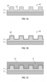
- FIG. 1A is a cross-sectional view of a flexible substrate having a patterned surface, according to one embodiment.
- the patterned surface 40 is formed on a major surface of the flexible substrate 2.
- the patterned surface 40 includes one or more recessed features 42 and one or more plateau features 44 adjacent to the recessed features 42.
- the plateau features 44 may form a mesh configuration such as the mesh 52 shown in FIG. 7 .
- a mesh described herein is typically understood to mean a pattern geometry having connected traces that are separated by open areas 54 to form cells.
- Illustrative examples of meshes with linear traces include, for example, those having hexagonal and square cells.
- the open area of the mesh can be, for example, greater than 90%, greater than 95%, or greater than 98%.
- the plateau features 44 can have an average line width in a range, for example, about 50 nm to about 5 microns, or about 100 nm to about 3 microns; and an average height in a range, for example, about 50 nm to about 5 microns, or about 100 nm to about 3 microns.
- the substrate 2 can be a flexible substrate, for example, a web of indefinite length polymeric material.
- the flexible substrate or web may be stretched (e.g., along a machine direction and/or a cross direction) when moving along a web path.
- the flexible substrate may include, for example, polyethylene terephthalate (PET), polyethylene, polystyrene, polyurethane, etc.
- PET polyethylene terephthalate
- the processes described herein can be carried out on a roll-to-roll apparatus including one or more rollers to convey the web along the web path.
- the substrate 2 may have a thickness of, for example, about 2 mm or less, about 1 mm or less, about 500 microns or less, or about 200 microns or less.
- the patterned surface 40 can be directly formed on the flexible substrate 2. In the depicted embodiment of FIG. 1A , the patterned surface 40 is formed on a patterned layer 4 that is disposed on the substrate 2.
- the patterned surface 40 can be formed on the substrate 2 by a micro-replication process.
- a layer of curable material can be provided onto the substrate 2 to form the patterned layer 4.
- the curable material may include, for example, polydimethylsiloxane (PDMS), epoxy, UV-curable acrylate resin, etc.
- a micro-replication stamp can be provided to press against the layer of curable material to create replicated features thereon.
- the curable material can be cured with various methods including, e.g., thermal, UV, e-beam radiation, etc. It is to be understood that the patterned surface 40 can be formed on the substrate 2 by any suitable methods such as, for example, embossing, micro-molding, micro-matching, laser etching, 3D printing, etc.
- the patterned layer 4 can include one or more release coating materials that exhibit a relatively low surface adhesion strength.
- release coating materials can include, for example, siloxanes, silicones, polytetrafluoroethylene, etc.
- the patterned surface 40 can be treated to lower the surface adhesion strength thereof.
- the patterned surface 40 of FIG. 1A is treated to form a release coating 46 thereon, according to one embodiment.
- the release coating 46 can be formed by a plasma deposition process.
- a gaseous hexamethyldisiloxane (HMDSO) can be introduced into a reaction chamber, and in the presence of a plasma to form a release coating on the patterned surface 40.
- the release coating may have a thickness, for example, less than about 500 nm, less than about 200 nm, or less than 100 nm.
- An exemplary plasma deposition process and apparatus is described in WO 2018/005109 (Yu et al ,), which is incorporated herein by reference.
- a liquid solution can be provided onto the patterned surface 40 to selectively form a releasable solid layer thereon.
- a liquid solution 6 is provided onto the patterned surface 40.
- the liquid solution 6 fills in the recessed features 42 and covers the plateau features 44.
- the liquid solution 6 has a surface level 61 that is higher than the plateau features 44. It is to be understood that in some embodiments, the liquid solution 6 may have the surface level 61 lower than the plateau features 44 and be present only in the recessed features 42.
- the liquid solution 6 may be a solution of poly(vinyl alcohol) (PVA) in water. It is to be understood that the liquid solution may include other solutes such as, for example, Polyvinyl butyral (PVB), curable acrylate, film formers, etc.
- PVA poly(vinyl alcohol)
- the liquid solution can be solubilized in any combination of common solvents such as water, isopropyl alcohol, methyl ethyl ketone, hexanes, ethyl acetate.
- the surface energy of the liquid composition can be modified by adding surfactants such as, for example, Polyethylene glycol p-(1,1,3,3-tetramethylbutyl)-phenyl ether (commercially available from Sigma-Aldrich Chemical company, Milwaukee, WI under the trade name Triton TM X-100).
- surfactants such as, for example, Polyethylene glycol p-(1,1,3,3-tetramethylbutyl)-phenyl ether (commercially available from Sigma-Aldrich Chemical company, Milwaukee, WI under the trade name Triton TM X-100).
- the liquid solution 6 is then solidified to form a releasable solid layer 62 in the recessed features 42.
- the liquid solution 6 can be solidified by drying at a temperature, for example, about 25 °C to about 175 °C, or about 50 °C to about 100 °C.
- the patterned surface 40 has a relative low surface adhesion strength such that the solid layer 62 is separable or releasable from the recessed features 42, for example, by peeling or washing.
- a solidifying product residue 64 remains on the plateau features 44 after the solidifying.
- the solidifying product residue 64 has a dry thickness thinner that of the solid layer 62 in the recessed features.
- the solidifying product residue 64 may have a dry thickness, for example, about 1 ⁇ 2 or less, about 1/3 or less, about 1/5 or less, or about 1/10 or less of the dry thickness of solid layer 62 in the recessed features.
- the plateau features 44 each have a planar top surface.
- the plateau features 44 can have various protrusive shapes such as, for example, a prismatic or pyramidal shape, a hemispherical shape, a bullet-like shape, etc.
- Various protrusive features were described in U.S. Patent No. 8,703,232 (Stay et al. ), which is incorporated herein by reference.
- the plateau features 44 may have a protrusive shape that allows the liquid solution 6 to flow from the plateau features into the recessed features 42 to reduce the amount of solidifying product residue 64 on the plateau features 44.
- the plateau features 44 may have hydrophobic surface characteristics that repel the liquid solution 6 to flow from the plateau features into the recessed features.
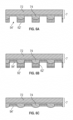
- FIG. 2A illustrates a process of providing a metal layer 8 to cover the patterned surface of FIG. 1D , according to one embodiment.
- a first portion 82 of the metal layer 8 is disposed in the recessed features 42; and a second portion 84 of the metal layer 8 is disposed on the top surface of plateau features 44.
- the layer of metal 8 can be formed by any desired processes including, for example, evaporating, sputtering, e-beam deposition, physical vapor deposition, chemical vapor deposition, liquid coating, etc.
- the metal layer may include multiple layers, for example, including a tie-layer to be in direct contact to the patterned surface, and a layer of another metal (e.g., copper, silver, gold, aluminum, etc.) on top of the tie-layer.
- the tie-layer also known as a glue or adhesion promoting layer can include chromium, chromium oxide, ITO, AZO, nickel, titanium, etc. It is to be understood that the metal layer may include any suitable electrically conductive materials.
- the metal layer 8 can have an average thickness of, for example, about 0.01 to about 2 micrometers, about 0.02 to about 1 micrometer, or about 0.025 to about 0.5 micrometers.
- the metal layer 8 can be continuous, have one or more surfaces conformal with the surface morphology of the patterned surface, and have a generally uniform thickness.
- the metal layer 8 may have a non-uniform thickness. For example, as illustrated in FIG. 2A , the metal layer 8 at the step 66 may have a decreased thickness or even be discontinued.
- a lift-off process can be performed to remove the releasable solid layer 62 in the recessed features along with the metal layer 82 thereon from the patterned surface.
- the remaining metal layer 84 on the patterned surface 40 forms a metal pattern, as shown in FIG. 2B .
- the solid layer 62 can be a water-soluble polymer layer that can be removed from the patterned surface 40 by, for example, pressure washing, ultrasonic washing, etc.
- the solid layer 62 includes poly(vinyl alcohol) (PVA)
- PVA poly(vinyl alcohol)
- the solid layer 62 can be dissolved and released from the substrate by water washing.
- the solid layer 62 can be removed by peeling.
- a curable resin layer for example, an acylate resin, can be overcast on the patterned surface 40. The curable resin layer can be cured and peeled from the patterned surface 40 along with the metal layer and the releasable solid layer in the recessed features.
- the curable resin material can have a suitable affinity to the metal layer such that the metal layer on top of the plateaus can remain on the patterned surface, while the releasable solid layer can be removed along with the metal layer thereon.
- the metal layer can be applied in a manner such that it adheres more strongly to the patterned surface, such as, for example, deposition using sputtering and/or using a tie layer.
- the releasable solid layer 62 can be any appropriate resist layer that can be removed from the patterned surface 40 by applying, for example, a solvent, heat, cooling, peeling, etc.
- the release coating 46 underneath the solid layer 62 in the recessed features can be completely or partially removed along with the solid layer 62.
- the solidifying product residue 64 remaining on the plateau features 44 after the solidifying can be removed before providing a metal layer on the plateau features.
- the residue 64 has been removed from the plateau features 44' by etching. Any suitable etching processes can be used, including, for example, reactive ion etching (RIE) such as oxygen or octofluoropropane plasma etching.
- RIE reactive ion etching
- the etching process can continue to remove the underneath release coating 46 (see FIG. 1B ) to expose the top surface of the plateau features 44.
- the RIE can remove the solidifying product residue and then modify the chemistry of the underneath release coating 46.
- the etching may also slightly reduce the thickness of the solid layer 62' in the recessed features.
- the thickness of the solid layer 62' can be reduced by, e.g., less than 20%, less than 10%, or less than 5%.
- the etching process used herein can be used to modify the chemistry of the release coating 46 (on the plateau features). Such modification can be beneficial for improving the adhesion of a metal layer disposed thereon.
- the etching process used herein can be well controlled such that it may not cause cross-linking in the releasable solid layer which may cause the solid layer to adhere more strongly to the substrate and be less soluble in water.
- the processes described herein can be technically advantageous over the traditional thermal imprint lithography process such as described in U.S. Patent No. 5,772,905 (Chou et al. ), where a heavy reactive-ion etching process may deteriorate the substrate surface and the thereafter formed metal/substrate interface.
- FIG. 3B illustrates a process of providing a metal layer 8' to cover the patterned surface of FIG. 3A , according to one embodiment.
- a first portion 82' of the metal layer 8' is disposed on the releasable solid layer 62' in the recessed features; and a second portion 84' of the metal layer 8' is directly disposed on the top surface of plateau features 44'.
- a lift-off process can be performed to remove the solid layer 62' in the recessed features along with the metal layer 82' thereon.
- FIG. 3C is a cross-sectional view of the metal pattern 84' on the plateau features 44'.
- a patterned surface covered with selectively formed, releasable solid layer such as the structure shown in FIG. 1D can be used as a molding surface to make metallized patterns. It is to be understood that the patterned surface can be made of other suitable materials such as, for example, metal.
- FIG. 4A illustrates a process of providing a transfer layer onto the patterned surface of FIG. 1D , according to one embodiment.
- the solidifying product residue 64 remaining on the plateau features 44 after the solidifying can be removed before providing a transfer layer thereon, such as the embodiment depicted in FIG. 3A .
- the transfer layer 7 includes an adhesive layer 74 in direct contact to the patterned surface of the patterned layer 4.
- the adhesive layer 74 is supported by a flexible backing layer 72.
- the adhesive layer 74 can be formed by providing a curable liquid onto the patterned surface to form a cured product.
- the adhesive layer can be at least partially formed by resolubilizing the releasable solid layer 62, and using the resolubilized layer as at least a portion of the adhesive layer.
- the adhesive layer can also be solvent coated onto the backing 72 or on top of the patterned surface.
- the layer of adhesive 74 can include any suitable adhesive materials having the desired properties.
- the layer of adhesive 74 can be peelable or stretch releasable and peelable from the patterned surface of the substrate 2.
- the adhesive can include at least one of rubber, silicone, or acrylic based adhesives.
- the adhesive can include tackified rubber adhesives, such as natural rubber; olefins; silicones, such as silicone polyureas or silicone block copolymers; synthetic rubber adhesives such as polyisoprene, polybutadiene, and styrene-isoprene-styrene, styrene-ethylene-butylene- styrene and styrene-butadiene-styrene block copolymers, and other synthetic elastomers; and tackified or untackified acrylic adhesives such as copolymers of isooctylacrylate and acrylic acid, which can be polymerized by radiation, solution, suspension, or emulsion techniques; polyurethanes; silicone block copolymers; and combinations of the above.
- tackified rubber adhesives such as natural rubber; olefins; silicones, such as silicone polyureas or silicone block copolymers
- synthetic rubber adhesives such as polyiso
- the adhesive can be, for example, any of the adhesives described in any of the following patent applications, all of which are incorporated by reference herein: PCT Patent Publication Nos. 2015/035556 , 2015/035960 , and U.S. Patent Publication NO. 2015/034104 .
- the backing layer 72 may have sufficient flexibility so that the transfer layer 7 can provide conformability and resiliency properties which are helpful when the adhesive layer 74 is adhered to the patterned surface of the patterned layer 7 and when it is removed therefrom by peeling.
- the flexible backing layer 72 can include a flexible polymeric film.
- the flexible backing layer 72 may include, for example, polyethylene terephthalate (PET), polyethylene, polystyrene, polyurethane, etc.
- PET polyethylene terephthalate
- PET polyethylene
- polystyrene polyurethane
- the processes described herein can be carried out on a roll-to-roll apparatus including one or more rollers to convey the web along the web path.
- the transfer layer 7 may have a thickness of, for example, about 2 mm or less, about 1 mm or less, about 500 microns or less, or about 200 microns or less.
- FIG. 4B illustrates a cross-sectional view of the transfer layer 7 which forms a patterned construction 54.
- the patterned construction 54 can be a negative relief of the patterned surface 40 of FIG. 1A .
- the patterned construction 54 includes protrusive features 542 which correspond to the recessed features 42 of the patterned surface 40 of FIG. 1A , and recesses 544 which correspond to the plateau features 44 of FIG. 1A .
- the protrusive features 542 has a top portion including the releasable solid layer 62, and a bottom potion including the material of the adhesive layer 74.
- the solidifying product residue 64 is attached to the bottom surface of the recesses 544. It is to be understood that the release coating 46 (see FIG. 1B ) may be at least partially transferred along the solid layer 62 and the solidifying product residue 64 from the patterned layer 4 to the transfer layer 7, covering the solid layer 62 and the solidifying product residue 64, respectively.
- the recesses 544 may form a mesh configuration such as the mesh 52 shown in FIG. 7 .
- a mesh described herein is typically understood to mean a pattern geometry having connected traces that are separated by open area to form cells.
- Illustrative examples of meshes with linear traces include, for example, those having hexagonal and square cells.
- the recesses 544 can have an average line width in a range, for example, about 50 nm to about 5 microns, and an average depth in a range, for example about 50 nm to about 5 microns.
- FIG. 5A illustrates a cross-sectional view of a metal layer on the patterned construction 54 of FIG. 4B , according to one embodiment.
- the metal layer includes a first portion 92 disposed on the top surface of the protrusive features 542, and a second portion 94 disposed on the bottom surface of the recesses 544.
- the layer of metal can be formed by any desired process including, for example, evaporating, sputtering, e-beam deposition, physical vapor deposition, chemical vapor deposition, liquid coating, etc.
- the metal layer may include multiple layers, for example, including a tie-layer (e.g., nickel or titanium) to be in direct contact to the patterned surface, and a layer of another metal (e.g., copper, silver, gold, aluminum, etc.) on top of the tie-layer.
- a tie-layer e.g., nickel or titanium
- another metal e.g., copper, silver, gold, aluminum, etc.
- the first portion 92 and the second portion 94 of the metal layer are disconnected with each other. That is, the metal layer is not conformally formed on the sides of the protrusive features 542. It is to be understood that the metal layer may be formed at least partially on the sides of the protrusive features 542 with a decreased thickness.
- the metal layer 94 in the recesses 544 can have an average thickness of, for example, about 0.01 to about 2 micrometers, about 0.02 to about 1 micrometer, or about 0.025 to about 0.5 micrometers. In some embodiments, the metal layer 94 in the recesses 544 can be continuous, have one or more surfaces conformal with the surface morphology of the bottom surfaces of the recesses 544, and have a generally uniform thickness. In some embodiments, the metal layer 94 may have a non-uniform thickness.
- a lift-off process can be performed to remove the solid layer 62 on the protrusive features 542 along with the metal layer 92 thereon.
- the solid layer 62 can be a water-soluble polymer layer that can be removed from the transfer layer 7 by, for example, pressure washing.
- PVA poly(vinyl alcohol)
- the solid layer 62 can be dissolved and released from the substrate by water washing.
- the solid layer 62 can be removed by peeling.
- a curable resin layer can be overcast on the transfer layer 7. The curable resin layer can be cured and peeled from the patterned construction 54 along with the metal layer and the solid layer on the protrusive features.
- FIG. 5B is a cross-sectional view of the remaining metal pattern 94 in the recesses 544.
- the solidifying product residue 64 remaining in the recesses 544 of the transfer layer 7 can be removed before providing a metal layer onto the transfer layer 7.
- the solidifying product residue 64 has been removed from the bottom surface of the recesses 544 by etching. Any suitable etching processes can be used, including, for example, reactive ion etching (RIE) such as oxygen or oxtafluoropropane plasma etching.
- RIE reactive ion etching
- the etching can first remove the release coating 46 on the surface (if applicable), and continue to remove the underneath solidifying product residue 64 to expose the bottom surface of the recesses 544.
- the etching can also slightly reduce the thickness of the solid layer 62 of the protrusive features 522. In some embodiments, the thickness of the solid layer 62 can be reduced by, e.g., less than 20%, less than 10%, or less than 5%.
- FIG. 6B illustrates a process of providing a metal layer to cover the patterned construction 54' of FIG. 6A , according to one embodiment.
- a first portion 92' of the metal layer is disposed on the solid layer 62 of the protrusive features; and a second portion 94' of the metal layer is directly disposed on the bottom surface of the recesses 544'.
- a lift-off process can be performed to remove the solid layer 62' along with the metal layer 92' thereon from the transfer layer 7.
- FIG. 6C is a cross-sectional view of the metal pattern 94' in the recesses 544' of the transfer layer 7.
- the metal patterns described herein can be applied to various devices.
- the metal patterns can be disposed only on plateau features of a patterned surface to form a mesh shape on a flexible substrate.
- the metal patterns can be disposed only in recesses of a patterned surface to form a mesh shape on a flexible substrate.
- the metal pattern can have a thickness, for example, about 20 nm to 500 nm.
- the flexible substrate having the patterned surface that supports the metal pattern can be transparent.
- the patterned surface with the metal pattern can be back-filled with a material that is index-matched to the top layer of the structured layer.
- Exemplary backing filling materials were described in U.S. Patent No. 8703232 (Stay et al. ), which is incorporated herein by reference.
- a pattern of other materials can be formed on the flexible substrate in similar manners.
- the materials for such a pattern may include ceramics, inks, or any suitable optical materials.
- similar processes/methods can be used to make suitable patterns other than a mesh on a flexible substrate.
- the processes described herein can be performed in a continuous or roll-to-roll manner.
- Exemplary continuous or roll-to-roll micro-replication processes were described in U.S. Patent No. 9759663 (Halverson et. al.).
- Exemplary continuous or roll-to-roll processes of plasma coating and etching were described in U.S. Patent No. 8460568 (David et. al.).
- Exemplary continuous or roll-to-roll processes of coating and drying were described in U.S.
- Patent No 8623140 (Yapel et al ). Lamination and stripping of webs can be added after the coating step. Exemplary continuous or roll-to-roll processes of metal deposition were described in U.S. Patent No. 6172810 (Fleming et al ).
- Embodiment 1 is a method of forming a metal pattern on a flexible substrate, the method comprising:
- Embodiment 2 is the method of embodiment 1, further comprising treating the patterned surface to form a release coating thereon before coating the liquid solution.
- Embodiment 3 is the method of embodiment 1 or 2, wherein the liquid layer also covers the plateau features on the patterned surface.
- Embodiment 4 is the method of any one of embodiments 1-3, wherein a solidifying product residue remains on the plateau features after the solidifying, the solidifying product residue has a dry thickness that is at most 1 ⁇ 2 the thickness of the solid layer in the recessed features.
- Embodiment 5 is the method of embodiment 4, wherein the solidifying product residue has a dry thickness of about 200 nm or less.
- Embodiment 6 is the method of any one of embodiments 2-5, wherein the etching is capable of removing or modifying the release coating.
- Embodiment 7 is the method of any one of embodiments 1-6, wherein the metal layer is provided by sputtering deposition with a tie layer.
- Embodiment 8 is the method of any one of embodiments 1-7, wherein removing the solid layer further comprises overcoating a curable resin on the metal layer and curing the curable resin to form a cured resin layer.
- Embodiment 9 is the method of embodiment 8, further comprising peeling the cured resin layer to remove the solid layer along with the metal layer thereon in the recessed features from the flexible substrate.
- Embodiment 10 is the method of any one of embodiments 1-9, wherein providing a patterned surface on the flexible substrate comprises forming micro-replicated features on the flexible substrate.
- Embodiment 11 is the method of embodiment 9, wherein the micro-replicated features are formed on a patterned surface layer of the flexible substrate.
- Embodiment 12 is the method of any one of embodiments 2-10, wherein the release coating is formed by a plasma deposition process using hexamethyldisiloxane (HMDSO).
- HMDSO hexamethyldisiloxane
- Embodiment 13 is the method of any one of embodiments 1-12, wherein the liquid solution comprises poly(vinyl alcohol) (PVA).
- PVA poly(vinyl alcohol)
- Embodiment 14 is the method of any one of embodiments 1-13, wherein the metal pattern on the plateau features of the flexible substrate forms a mesh shape having an open area greater than 95%.
- Embodiment 15 is the method of any one of embodiments 1-14, wherein the patterned surface with the metal pattern thereon is back-filled with a material that is index-matched to the patterned surface.
- Embodiment 16 is a device made according to the method of any one of embodiments 1-15, the device comprising:
- Embodiment 17 is a method of forming a metal pattern, the method comprising:
- Embodiment 18 is the method of embodiment 17, further comprising treating the patterned surface to form a release coating thereon.
- Embodiment 19 is the method of embodiment 17 or 18, wherein the transfer layer comprises an adhesive layer which is a curing product of a curable liquid that is applied onto the patterned surface.
- Embodiment 20 is the method of embodiment 19, wherein the transfer layer further comprises a flexible backing layer to support the adhesive layer.
- Embodiment 21 is the method of any one of embodiments 17-20, further comprising etching the patterned surface before providing the transfer layer.
- Embodiment 22 is the method of any one of embodiments 17-21, further comprising etching the patterned construction before providing the metal layer on the patterned construction.
- Embodiment 23 is the method of any one of embodiments 17-22, wherein the metal layer is provided by sputtering deposition with a tie layer.
- Embodiment 24 is the method of any one of embodiments 17-23, wherein the solid layer and the metal layer thereon are removed by water washing.
- Embodiment 25 is the method of any one of embodiments 17-24, wherein the solid layer and the metal layer thereon are removed by peeling.
- Embodiment 26 is the method of any one of embodiments 17-25, wherein the patterned surface with the metal pattern thereon is back-filled with a material that is index-matched to the patterned surface.
- Embodiment 28 is a method of forming an electrically conductive mesh pattern on a flexible substrate, the method comprising:
- Embodiment 29 is the method of embodiment 28, further comprising providing a metal layer to cover the patterned surface; and removing the solid layer along with the metal layer thereon in the recesses to form a mesh metal pattern on the plateau features.
- Embodiment 30 is the method of embodiment 28, further comprising:
- Table 1 provides abbreviations and a source for all materials used in the Examples below: Table 1 Abbreviation Description Source PVA Polyvinyl alcohol 9,000-10,000 MW 80% hydrolyzed Sigma-Aldrich Chemiacl Company, Milwaukee, WI Mel454 DuPont Tejin Films Melinex TM 454 polyester film (50.8um thick) DuPont, Wilmington, DE COP Cyclic olefin copolymer film Zeonor ZF16-100 Zeon Chemicals, Louisville, KY Tergitol Tergitol TM 15-s-7 Sigma-Aldrich Chemiacl Company, Milwaukee, WI HMDSO Hexamethyldisiloxane Sigma-Aldrich Chemiacl Company, Milwaukee, WI
- Matture 1 is a combination of 75wt% of an aliphatic urethane diacrylate, 25 wt% of a diacrylate and 0.5% photoinitiator.
- Matture 2 is a solution of 3-10% PVA, 10% isopropyl alcohol, 0.05% Tergitol in DI water.
- Both patterned surfaces were formed by roll-to-roll microreplication.
- Mel 454 was coated with Mixture 1, nipped against a structured tool, cured using ultra-violet lights, and then peeled from the tool.
- a first pattern is a "pseudorandom curved" pattern depicted in figure 7 .
- the lines in the figure represent features which have almost vertical side-walls, are 2 microns tall and 2 microns wide.
- the average pitch of the cells is 200 microns.
- a second pattern is a hexagonal pattern depicted in FIG. 1 of U.S. Patent Publication NO. 2013/0306359 .
- the lines in the figure represent features which are 2 microns tall, 2 microns wide at the peak, and 4 microns wide at the base.
- the pitch of the hexagons is 200 microns.
- layer(s) were added or reduced using known coating and etching techniques.
- HMDSO Hexamethyldisiloxane
- the chamber has a central cylindrical powered electrode with a surface area of 18.3 ft 2 .
- the reactor chamber was pumped down to a base pressure of less than 1.3 Pa (2 mTorr).
- HMDSO was evaporated into the chamber through a 1 ⁇ 2 tube without restriction.
- Treatment was carried out using a plasma enhanced CVD method by coupling RF power into the reactor at a frequency of 13.56 MHz and an applied power of 2000 watts. Treatment time was controlled by moving the micro-structured film through the reaction zone at a rate of 30 feet per minute.
- a Meyer rod technique was used to coat a solution on a piece part sample. Solution concentration and Meyer rod were adjusted to achieve the correct dry thickness. These solutions were allowed to dry at room temperature.
- a batch etching method was used to etch piece-part samples.
- a vacuum was pulled in a Plasmatherm Model 3032 capacitive plasma reactor and oxygen was flowed in at a rate of 500 standard cubic centemeters per minute.
- the reactor power was set to 1350 watts.
- the amount that was etched was controlled by adjusting the time the reactor is on.
- a roll-to-roll etching method was used to continuously etch. Samples were the etched in a home-built chamber that has a web path of approximately 3 meters. The speed of the web and the number of passes was adjusted to change the residence time in the reactor. Octafluoropropane was flowed in at a rate of 250 standard cubic centimeter per minute and oxygen was flowed in at a rate of 750 standard cubic centimeter per minute. The reactor power was set to 6000 watts.
- a pseudorandom curved pattern was plasma coated with HDMSO.
- Mixture 2 was die coated to a dry thickness of 0.5 microns.
- Silver was sputtered in a batch process to a thickness of 200 nanometers.
- the silver layer was laminated to Mel454 with Mixture 1, then cured with ultraviolet light, then peeled to remove the solid layer from the recessed features.
- a pseudorandom curved pattern was plasma coated with HDMSO.
- Mixture 2 was die coated to a dry thickness of 0.5 microns.
- Silver was sputtered in a batch process to a thickness of 200 nanometers. The substrate was placed under an ultrasonic horn for 10 seconds to remove the solid layer.
- a hexagonal pattern was plasma coated with HDMSO.
- Mixture 2 was die coated to a dry thickness of 1 micron.
- the patterned surface was roll-to-roll etched for 30 seconds.
- Silver was sputtered in a roll-to-roll process to a thickness of 200 nanometers.
- the silver layer was laminated to Mel454 with Mixture 1, then cured with ultraviolet light, then peeled to remove the solid layer from the recessed features.
- the metalized pattern from example 1.2 was back-filled with Mixture 1, laminated to COP, and cured with ultraviolet light.
- a hexagonal pattern was plasma coated with HDMSO.
- Mixture 2 was Meyer rod coated to a dry thickness of 1 microns.
- the pattern was etched in a batch process for 30 seconds.
- Silver was sputtered in a batch process to a thickness of 200 nanometers.
- the silver layer was laminated to Mel454 with Mixture 1, then cured with ultraviolet light, then peeled to remove the solid layer from the recessed features.
- a hexagonal pattern was plasma coated with HDMSO.
- Mixture 2 was die coated to a dry thickness of 0.5 microns.
- Silver was sputtered in a batch process to a thickness of 200 nanometers.
- the silver layer was laminated to Mel454 with Mixture 1, then cured with ultraviolet light, then peeled to remove the solid layer from the recessed features.
- Mixture 2 was Meyer rod coated to a dry thickness of 1 microns on a hexagonal pattern. The pattern was etched in a batch process for 30 seconds. Silver was sputtered in a batch process to a thickness of 200 nanometers. The silver layer was laminated to Mel454 with Mixture 1, then cured with ultraviolet light, then peeled to remove the solid layer from the recessed features.
- Table 2 Example number Pattern Plasma coating PVA dry thickness (um) Lamination resin Etch time Metal thickn ess (um) Metal deposition method Release method 8 Hexag onal Y 2 Mixture 1 30 200 Sputter Peel 9 Hexag onal Y 2 Mixture 1 0 200 Sputter Peel
- a hexagonal pattern was plasma coated with HDMSO.
- Mixture 2 was die coated to a dry thickness of 2 microns.
- the pattern was transferred to Mel454 by coating Mixture 1, curing with ultraviolet light, then peeling.
- the patterned construction was etched in a batch process for 30 seconds.
- Silver was sputtered in a batch process to a thickness of 200 nanometers.
- the silver layer was laminated to Mel454 with Mixture 1, then cured with ultraviolet light, then peeled to remove the solid layer from the recessed features.
- a hexagonal pattern was plasma coated with HDMSO.
- Mixture 2 was die coated to a dry thickness of 2 microns.
- the pattern was transferred to Mel454 by coating Mixture 1, curing with ultraviolet light, then peeling.
- Silver was sputtered in a batch process to a thickness of 200 nanometers.
- the silver layer was laminated to Mel454 with Mixture 1, then cured with ultraviolet light, then peeled to remove the solid layer from the recessed features.
- Example 8 contained more metal on the traces.
Landscapes
- Engineering & Computer Science (AREA)
- Microelectronics & Electronic Packaging (AREA)
- Manufacturing & Machinery (AREA)
- Laminated Bodies (AREA)
- Manufacturing Of Printed Wiring (AREA)
- Shaping Of Tube Ends By Bending Or Straightening (AREA)
- Manufacturing Of Printed Circuit Boards (AREA)
- ing And Chemical Polishing (AREA)
Applications Claiming Priority (3)
| Application Number | Priority Date | Filing Date | Title |
|---|---|---|---|
| US201862691459P | 2018-06-28 | 2018-06-28 | |
| PCT/IB2019/055466 WO2020003207A1 (en) | 2018-06-28 | 2019-06-27 | Methods of making metal patterns on flexible substrate |
| EP19825141.5A EP3815475A4 (de) | 2018-06-28 | 2019-06-27 | Verfahren zur herstellung von metallmustern auf einem flexiblen substrat |
Related Parent Applications (1)
| Application Number | Title | Priority Date | Filing Date |
|---|---|---|---|
| EP19825141.5A Division EP3815475A4 (de) | 2018-06-28 | 2019-06-27 | Verfahren zur herstellung von metallmustern auf einem flexiblen substrat |
Publications (2)
| Publication Number | Publication Date |
|---|---|
| EP4528444A2 true EP4528444A2 (de) | 2025-03-26 |
| EP4528444A3 EP4528444A3 (de) | 2025-10-15 |
Family
ID=68984514
Family Applications (2)
| Application Number | Title | Priority Date | Filing Date |
|---|---|---|---|
| EP19825141.5A Pending EP3815475A4 (de) | 2018-06-28 | 2019-06-27 | Verfahren zur herstellung von metallmustern auf einem flexiblen substrat |
| EP25155781.5A Pending EP4528444A3 (de) | 2018-06-28 | 2019-06-27 | Verfahren zur herstellung von metallmustern auf einem flexiblen substrat |
Family Applications Before (1)
| Application Number | Title | Priority Date | Filing Date |
|---|---|---|---|
| EP19825141.5A Pending EP3815475A4 (de) | 2018-06-28 | 2019-06-27 | Verfahren zur herstellung von metallmustern auf einem flexiblen substrat |
Country Status (5)
| Country | Link |
|---|---|
| US (2) | US11950372B2 (de) |
| EP (2) | EP3815475A4 (de) |
| CN (2) | CN112385321B (de) |
| TW (1) | TWI826477B (de) |
| WO (1) | WO2020003207A1 (de) |
Families Citing this family (6)
| Publication number | Priority date | Publication date | Assignee | Title |
|---|---|---|---|---|
| CN111999279B (zh) * | 2020-07-21 | 2021-09-21 | 北京邮电大学 | 一种基于小球阵列的柔性sers基底及其制备方法 |
| JP2023551717A (ja) * | 2020-12-02 | 2023-12-12 | スリーエム イノベイティブ プロパティズ カンパニー | マイクロカットパターン化された転写物品 |
| EP4271996B1 (de) | 2020-12-31 | 2025-12-24 | 3M Innovative Properties Company | Nanostrukturierte folien mit strukturierter oberflächenchemie |
| CN113503914B (zh) * | 2021-06-29 | 2023-11-17 | 西北工业大学 | 一种柔性传感器的制备方法 |
| CN117822334A (zh) * | 2023-12-27 | 2024-04-05 | 东莞光群雷射科技有限公司 | 一种利用图案转移制备表面金属化材料的方法 |
| CN121001253A (zh) * | 2025-10-24 | 2025-11-21 | 常州欣盛半导体技术股份有限公司 | 高深宽比的透明超细电路结构及其制造方法 |
Citations (9)
| Publication number | Priority date | Publication date | Assignee | Title |
|---|---|---|---|---|
| US5772905A (en) | 1995-11-15 | 1998-06-30 | Regents Of The University Of Minnesota | Nanoimprint lithography |
| US6172810B1 (en) | 1999-02-26 | 2001-01-09 | 3M Innovative Properties Company | Retroreflective articles having polymer multilayer reflective coatings |
| US8460568B2 (en) | 2008-12-30 | 2013-06-11 | 3M Innovative Properties Company | Method for making nanostructured surfaces |
| US20130306359A1 (en) | 2011-02-02 | 2013-11-21 | 3M Innovative Properties Company | Patterned Substrates With Darkened Multilayered Conductor Traces |
| US8623140B2 (en) | 2007-07-25 | 2014-01-07 | 3M Innovative Properties Company | System and method for making a film having a matte finish |
| US8703232B2 (en) | 2008-06-30 | 2014-04-22 | 3M Innovative Properties Company | Method of forming a microstructure |
| US20150034104A1 (en) | 2011-11-25 | 2015-02-05 | Shenzhen Bauway Technology Limited | Anion electronic cigarette |
| US9759663B2 (en) | 2009-11-23 | 2017-09-12 | 3M Innovative Properties Company | Microwell array articles and methods of use |
| WO2018005109A1 (en) | 2016-06-30 | 2018-01-04 | 3M Innovative Properties Company | Fluorocarbon release coating |
Family Cites Families (38)
| Publication number | Priority date | Publication date | Assignee | Title |
|---|---|---|---|---|
| US6114088A (en) * | 1999-01-15 | 2000-09-05 | 3M Innovative Properties Company | Thermal transfer element for forming multilayer devices |
| US6334960B1 (en) | 1999-03-11 | 2002-01-01 | Board Of Regents, The University Of Texas System | Step and flash imprint lithography |
| US6485884B2 (en) * | 2001-04-27 | 2002-11-26 | 3M Innovative Properties Company | Method for patterning oriented materials for organic electronic displays and devices |
| JP4095297B2 (ja) * | 2001-12-25 | 2008-06-04 | 大日本印刷株式会社 | 電磁波遮蔽シートの製造方法及び電磁波遮蔽シート |
| KR20060126433A (ko) * | 2003-09-01 | 2006-12-07 | 다이니폰 인사츠 가부시키가이샤 | 플라즈마 디스플레이용 전자파 차폐 필름 |
| JP4436646B2 (ja) * | 2003-09-25 | 2010-03-24 | 京セラ株式会社 | マイクロ空間配線基板及びその製造方法 |
| MXPA06006738A (es) | 2003-12-19 | 2006-08-31 | Univ North Carolina | Metodos para fabricar micro- y nano-estructuras aisladas utilizando litografia suave o de impresion. |
| JP4386759B2 (ja) * | 2004-02-26 | 2009-12-16 | 大日本印刷株式会社 | 水圧転写シート及び金属調成形品の製造方法 |
| JP4160569B2 (ja) * | 2004-05-31 | 2008-10-01 | 株式会社東芝 | 半導体装置の製造方法 |
| CN2818150Y (zh) * | 2005-02-05 | 2006-09-20 | 汕头市东田转印有限公司 | 一种转印膜 |
| US7591641B2 (en) * | 2005-03-22 | 2009-09-22 | Canon Kabushiki Kaisha | Mold and process of production thereof |
| JP2006303454A (ja) * | 2005-03-22 | 2006-11-02 | Canon Inc | ナノインプリント用モールドとその製造方法、凹凸パターンの転写方法、凹部を有する部材の製造方法 |
| JP2007042887A (ja) * | 2005-08-03 | 2007-02-15 | Bridgestone Corp | 光透過性電磁波シールド性窓材及びその製造方法 |
| JP2010503993A (ja) * | 2006-09-19 | 2010-02-04 | モレキュラー・インプリンツ・インコーポレーテッド | リフトオフ・パターニング向けの向上したエッチング技法 |
| US8512581B2 (en) * | 2006-10-09 | 2013-08-20 | Solexel, Inc. | Methods for liquid transfer coating of three-dimensional substrates |
| JP2008311416A (ja) * | 2007-06-14 | 2008-12-25 | Dainippon Printing Co Ltd | 金属転写箔を用いた電磁波シールドメッシュの製造方法、及び電磁波シールドメッシュ |
| JP4927070B2 (ja) * | 2008-12-26 | 2012-05-09 | 日本写真印刷株式会社 | 透明導電性シートとその製造方法、加飾成形品 |
| JP5464574B2 (ja) | 2009-03-31 | 2014-04-09 | 日本写真印刷株式会社 | 透明導電性シートとその製造方法、加飾成形品 |
| JP2010266734A (ja) * | 2009-05-15 | 2010-11-25 | Dainippon Printing Co Ltd | 複合光学フィルタの製造方法 |
| JP4626721B1 (ja) * | 2009-09-02 | 2011-02-09 | ソニー株式会社 | 透明導電性電極、タッチパネル、情報入力装置、および表示装置 |
| US20120210749A1 (en) | 2011-02-22 | 2012-08-23 | Jiangwei Feng | Ion exchange using nitrates and nitrites to prevent optical degradation of glass |
| KR101451547B1 (ko) * | 2012-06-13 | 2014-10-15 | 아사히 가세이 이-매터리얼즈 가부시키가이샤 | 기능 전사체, 기능층의 전사 방법, 곤포물 및 기능 전사 필름 롤 |
| JPWO2014041904A1 (ja) * | 2012-09-13 | 2016-08-18 | 東レ株式会社 | 凹凸形状付積層体の製造方法および転写フィルム |
| TWI479175B (zh) * | 2013-01-15 | 2015-04-01 | Architek Material Co Ltd | 轉換結構、影像偵測裝置以及轉換結構之製備方法 |
| KR101598249B1 (ko) | 2013-01-29 | 2016-02-26 | 삼성전기주식회사 | 터치패널 |
| US9483147B2 (en) * | 2013-03-30 | 2016-11-01 | Shenzhen O-Film Tech Co., Ltd. | Monolayer touch screen and method for manufacturing the same |
| JP2015011746A (ja) * | 2013-06-28 | 2015-01-19 | 株式会社東芝 | パターン形成方法、それを用いた磁気記録媒体の製造方法、磁気記録媒体、及びスタンパーの製造方法 |
| CN104854580B (zh) | 2013-09-10 | 2018-09-28 | 华为技术有限公司 | 一种推荐方法和设备 |
| CN103513412B (zh) | 2013-09-16 | 2015-10-07 | 华为终端有限公司 | 潜望式镜头和终端设备 |
| US10537028B2 (en) * | 2014-06-30 | 2020-01-14 | 3M Innovative Properties Company | Metallic microstructures with reduced-visibility and methods for producing same |
| EP3209841B1 (de) * | 2014-10-20 | 2021-04-07 | 3M Innovative Properties Company | Isolierende verglasungseinheiten und mikrooptische schicht mit mikrostrukturiertem diffusor und verfahren |
| US10679964B2 (en) * | 2014-11-04 | 2020-06-09 | The Regents Of The University Of California | Solid-state wafer bonding of functional materials on substrates and self-aligned contacts |
| JP2016115178A (ja) * | 2014-12-16 | 2016-06-23 | 信越ポリマー株式会社 | 可撓性積層体及びその製造方法、静電容量式3次元センサ |
| JP6728569B2 (ja) * | 2015-03-30 | 2020-07-22 | 大日本印刷株式会社 | 転写シート及びこれを用いた加飾樹脂成形品 |
| CN105139963A (zh) * | 2015-07-01 | 2015-12-09 | 友达光电股份有限公司 | 一种电子装置及其制造方法 |
| JP6661343B2 (ja) * | 2015-11-26 | 2020-03-11 | 富士フイルム株式会社 | 転写材料、転写材料の製造方法、積層体、積層体の製造方法、静電容量型入力装置の製造方法、及び、画像表示装置の製造方法 |
| KR20180057089A (ko) * | 2016-11-21 | 2018-05-30 | 엘지이노텍 주식회사 | 전극 부재 및 이의 제조방법 |
| KR20210006436A (ko) * | 2018-05-25 | 2021-01-18 | 미쓰비시 세이시 가부시키가이샤 | 패턴 전사물의 제조 방법 |
-
2019
- 2019-06-27 CN CN201980042635.9A patent/CN112385321B/zh active Active
- 2019-06-27 CN CN202411220019.7A patent/CN119255498A/zh active Pending
- 2019-06-27 EP EP19825141.5A patent/EP3815475A4/de active Pending
- 2019-06-27 US US17/252,826 patent/US11950372B2/en active Active
- 2019-06-27 WO PCT/IB2019/055466 patent/WO2020003207A1/en not_active Ceased
- 2019-06-27 EP EP25155781.5A patent/EP4528444A3/de active Pending
- 2019-06-27 TW TW108122711A patent/TWI826477B/zh active
-
2024
- 2024-02-29 US US18/591,060 patent/US12309939B2/en active Active
Patent Citations (9)
| Publication number | Priority date | Publication date | Assignee | Title |
|---|---|---|---|---|
| US5772905A (en) | 1995-11-15 | 1998-06-30 | Regents Of The University Of Minnesota | Nanoimprint lithography |
| US6172810B1 (en) | 1999-02-26 | 2001-01-09 | 3M Innovative Properties Company | Retroreflective articles having polymer multilayer reflective coatings |
| US8623140B2 (en) | 2007-07-25 | 2014-01-07 | 3M Innovative Properties Company | System and method for making a film having a matte finish |
| US8703232B2 (en) | 2008-06-30 | 2014-04-22 | 3M Innovative Properties Company | Method of forming a microstructure |
| US8460568B2 (en) | 2008-12-30 | 2013-06-11 | 3M Innovative Properties Company | Method for making nanostructured surfaces |
| US9759663B2 (en) | 2009-11-23 | 2017-09-12 | 3M Innovative Properties Company | Microwell array articles and methods of use |
| US20130306359A1 (en) | 2011-02-02 | 2013-11-21 | 3M Innovative Properties Company | Patterned Substrates With Darkened Multilayered Conductor Traces |
| US20150034104A1 (en) | 2011-11-25 | 2015-02-05 | Shenzhen Bauway Technology Limited | Anion electronic cigarette |
| WO2018005109A1 (en) | 2016-06-30 | 2018-01-04 | 3M Innovative Properties Company | Fluorocarbon release coating |
Also Published As
| Publication number | Publication date |
|---|---|
| US20210161018A1 (en) | 2021-05-27 |
| EP3815475A1 (de) | 2021-05-05 |
| WO2020003207A1 (en) | 2020-01-02 |
| EP4528444A3 (de) | 2025-10-15 |
| TW202006834A (zh) | 2020-02-01 |
| US20240206076A1 (en) | 2024-06-20 |
| US11950372B2 (en) | 2024-04-02 |
| CN112385321A (zh) | 2021-02-19 |
| CN112385321B (zh) | 2024-09-24 |
| US12309939B2 (en) | 2025-05-20 |
| TWI826477B (zh) | 2023-12-21 |
| EP3815475A4 (de) | 2022-03-30 |
| CN119255498A (zh) | 2025-01-03 |
Similar Documents
| Publication | Publication Date | Title |
|---|---|---|
| US12309939B2 (en) | Methods of making metal patterns on flexible substrate | |
| US12363825B2 (en) | Patterned conductive article | |
| US8323520B2 (en) | Method for manufacturing fine concave-convex pattern and sheet for manufacturing fine concave-convex pattern | |
| US20070116934A1 (en) | Antireflective surfaces, methods of manufacture thereof and articles comprising the same | |
| WO2005103134A2 (en) | Roll-to-roll embossing tools and processes | |
| CN102470565A (zh) | 压印用树脂制模具及其制造方法 | |
| CN101939393A (zh) | 微米和/或纳米构造的保护或处理薄膜 | |
| Zhong et al. | Microstructure formation via roll-to-roll UV embossing using a flexible mould made from a laminated polymer–copper film | |
| TWI521194B (zh) | 積層結構體 | |
| TW201220974A (en) | Stencils for high-throughput micron-scale etching of substrates and processes of making and using the same | |
| US10155340B2 (en) | Mold, method for producing mold, and method for producing nanoimprint film | |
| Chan-Park et al. | Ultraviolet embossing for patterning high aspect ratio polymeric microstructures | |
| US12573766B2 (en) | Patterned article including metallic bodies | |
| CN111194256A (zh) | 蛾眼转印模、蛾眼转印模的制造方法及蛾眼结构的转印方法 | |
| WO2008082421A1 (en) | Antireflective surfaces, methods of manufacture thereof and articles comprising the same | |
| JP4401091B2 (ja) | 粘着シート及びその製造方法 | |
| WO2022144773A1 (en) | Apparatus and method for structured replication and transfer | |
| CN110289124B (zh) | 一种基于导电聚合物的柔性电极及其制备方法 | |
| KR20140117038A (ko) | 반사방지필름 및 그 제조 방법 | |
| CN102343670A (zh) | 光学膜的制备方法 | |
| TW201204537A (en) | Manufacturing method of an optical film |
Legal Events
| Date | Code | Title | Description |
|---|---|---|---|
| PUAI | Public reference made under article 153(3) epc to a published international application that has entered the european phase |
Free format text: ORIGINAL CODE: 0009012 |
|
| STAA | Information on the status of an ep patent application or granted ep patent |
Free format text: STATUS: REQUEST FOR EXAMINATION WAS MADE |
|
| 17P | Request for examination filed |
Effective date: 20250204 |
|
| AC | Divisional application: reference to earlier application |
Ref document number: 3815475 Country of ref document: EP Kind code of ref document: P |
|
| AK | Designated contracting states |
Kind code of ref document: A2 Designated state(s): AL AT BE BG CH CY CZ DE DK EE ES FI FR GB GR HR HU IE IS IT LI LT LU LV MC MK MT NL NO PL PT RO RS SE SI SK SM TR |
|
| REG | Reference to a national code |
Ref country code: DE Ref legal event code: R079 Free format text: PREVIOUS MAIN CLASS: G06F0003041000 Ipc: H05K0003040000 |
|
| RIC1 | Information provided on ipc code assigned before grant |
Ipc: H05K 1/02 20060101ALN20250509BHEP Ipc: H01B 5/14 20060101ALI20250509BHEP Ipc: H05K 3/04 20060101AFI20250509BHEP |
|
| PUAL | Search report despatched |
Free format text: ORIGINAL CODE: 0009013 |
|
| AK | Designated contracting states |
Kind code of ref document: A3 Designated state(s): AL AT BE BG CH CY CZ DE DK EE ES FI FR GB GR HR HU IE IS IT LI LT LU LV MC MK MT NL NO PL PT RO RS SE SI SK SM TR |
|
| RIC1 | Information provided on ipc code assigned before grant |
Ipc: H05K 3/04 20060101AFI20250905BHEP Ipc: H01B 5/14 20060101ALI20250905BHEP Ipc: H05K 1/02 20060101ALN20250905BHEP |