EP4510171A1 - Surface treatment composition and method for producing wafer - Google Patents
Surface treatment composition and method for producing wafer Download PDFInfo
- Publication number
- EP4510171A1 EP4510171A1 EP23788243.6A EP23788243A EP4510171A1 EP 4510171 A1 EP4510171 A1 EP 4510171A1 EP 23788243 A EP23788243 A EP 23788243A EP 4510171 A1 EP4510171 A1 EP 4510171A1
- Authority
- EP
- European Patent Office
- Prior art keywords
- surface treatment
- treatment composition
- mass
- group
- wafer
- Prior art date
- Legal status (The legal status is an assumption and is not a legal conclusion. Google has not performed a legal analysis and makes no representation as to the accuracy of the status listed.)
- Withdrawn
Links
Images



Classifications
-
- H—ELECTRICITY
- H10—SEMICONDUCTOR DEVICES; ELECTRIC SOLID-STATE DEVICES NOT OTHERWISE PROVIDED FOR
- H10W—GENERIC PACKAGES, INTERCONNECTIONS, CONNECTORS OR OTHER CONSTRUCTIONAL DETAILS OF DEVICES COVERED BY CLASS H10
- H10W74/00—Encapsulations, e.g. protective coatings
- H10W74/01—Manufacture or treatment
-
- B—PERFORMING OPERATIONS; TRANSPORTING
- B05—SPRAYING OR ATOMISING IN GENERAL; APPLYING FLUENT MATERIALS TO SURFACES, IN GENERAL
- B05D—PROCESSES FOR APPLYING FLUENT MATERIALS TO SURFACES, IN GENERAL
- B05D1/00—Processes for applying liquids or other fluent materials
- B05D1/60—Deposition of organic layers from vapour phase
-
- C—CHEMISTRY; METALLURGY
- C09—DYES; PAINTS; POLISHES; NATURAL RESINS; ADHESIVES; COMPOSITIONS NOT OTHERWISE PROVIDED FOR; APPLICATIONS OF MATERIALS NOT OTHERWISE PROVIDED FOR
- C09D—COATING COMPOSITIONS, e.g. PAINTS, VARNISHES OR LACQUERS; FILLING PASTES; CHEMICAL PAINT OR INK REMOVERS; INKS; CORRECTING FLUIDS; WOODSTAINS; PASTES OR SOLIDS FOR COLOURING OR PRINTING; USE OF MATERIALS THEREFOR
- C09D5/00—Coating compositions, e.g. paints, varnishes or lacquers, characterised by their physical nature or the effects produced; Filling pastes
-
- C—CHEMISTRY; METALLURGY
- C09—DYES; PAINTS; POLISHES; NATURAL RESINS; ADHESIVES; COMPOSITIONS NOT OTHERWISE PROVIDED FOR; APPLICATIONS OF MATERIALS NOT OTHERWISE PROVIDED FOR
- C09D—COATING COMPOSITIONS, e.g. PAINTS, VARNISHES OR LACQUERS; FILLING PASTES; CHEMICAL PAINT OR INK REMOVERS; INKS; CORRECTING FLUIDS; WOODSTAINS; PASTES OR SOLIDS FOR COLOURING OR PRINTING; USE OF MATERIALS THEREFOR
- C09D7/00—Features of coating compositions, not provided for in group C09D5/00; Processes for incorporating ingredients in coating compositions
- C09D7/20—Diluents or solvents
-
- H—ELECTRICITY
- H10—SEMICONDUCTOR DEVICES; ELECTRIC SOLID-STATE DEVICES NOT OTHERWISE PROVIDED FOR
- H10P—GENERIC PROCESSES OR APPARATUS FOR THE MANUFACTURE OR TREATMENT OF DEVICES COVERED BY CLASS H10
- H10P14/00—Formation of materials, e.g. in the shape of layers or pillars
-
- H—ELECTRICITY
- H10—SEMICONDUCTOR DEVICES; ELECTRIC SOLID-STATE DEVICES NOT OTHERWISE PROVIDED FOR
- H10P—GENERIC PROCESSES OR APPARATUS FOR THE MANUFACTURE OR TREATMENT OF DEVICES COVERED BY CLASS H10
- H10P70/00—Cleaning of wafers, substrates or parts of devices
- H10P70/10—Cleaning before device manufacture, i.e. Begin-Of-Line process
- H10P70/15—Cleaning before device manufacture, i.e. Begin-Of-Line process by wet cleaning only
-
- H—ELECTRICITY
- H10—SEMICONDUCTOR DEVICES; ELECTRIC SOLID-STATE DEVICES NOT OTHERWISE PROVIDED FOR
- H10P—GENERIC PROCESSES OR APPARATUS FOR THE MANUFACTURE OR TREATMENT OF DEVICES COVERED BY CLASS H10
- H10P70/00—Cleaning of wafers, substrates or parts of devices
- H10P70/20—Cleaning during device manufacture
-
- H—ELECTRICITY
- H10—SEMICONDUCTOR DEVICES; ELECTRIC SOLID-STATE DEVICES NOT OTHERWISE PROVIDED FOR
- H10P—GENERIC PROCESSES OR APPARATUS FOR THE MANUFACTURE OR TREATMENT OF DEVICES COVERED BY CLASS H10
- H10P70/00—Cleaning of wafers, substrates or parts of devices
- H10P70/50—Cleaning of wafers, substrates or parts of devices characterised by the part to be cleaned
-
- H—ELECTRICITY
- H10—SEMICONDUCTOR DEVICES; ELECTRIC SOLID-STATE DEVICES NOT OTHERWISE PROVIDED FOR
- H10W—GENERIC PACKAGES, INTERCONNECTIONS, CONNECTORS OR OTHER CONSTRUCTIONAL DETAILS OF DEVICES COVERED BY CLASS H10
- H10W42/00—Arrangements for protection of devices
Definitions
- the present invention relates to a surface treatment composition and a method for producing a wafer.
- a water-repellent protective film on the pattern surface is known to be effective as a method for preventing pattern collapse.
- the water repelling property needs to be imparted without drying the pattern surface, thus, a water-repellent protective film is formed by supplying a chemical solution for forming a water-repellent protective film, which is capable of making a pattern surface water repellent, to the pattern surface in a state where a cleaning liquid or the like is being held thereon, in order to replace the cleaning liquid or the like with the above-described chemical solution.
- Patent Document 1 describes a surface treatment composition including a silylating agent as well as diethyl carbonate and propylene carbonate as solvents (Example 5 of Patent Document 1).
- Patent Document 1 International Publication No. 2019/193967
- the present inventors found that the above-described surface treatment composition easily increases the water contact angle as a result of using a silicon compound such as trialkylsilylamine as a silylating agent together with a hydrocarbon solvent having a content of 97% by mass or more in a solvent as the solvent and, through subsequent studies, further found that it is possible to maintain a contact angle that is high in practice as long as the content of the hydrocarbon solvent in the solvent is 75% by mass or more, thereby completing the present invention.
- the surface treatment composition and method for producing a wafer described below are provided.
- a surface treatment composition that easily increases a water contact angle and a method for producing a wafer using the same are provided.
- the surface treatment composition of the present embodiment is supplied as vapor to a surface of a wafer having an uneven pattern on the surface and is used for forming a water-repellent protective film on the surface.
- This surface treatment composition includes a silylating agent and a solvent and is formed such that the silylating agent includes a silicon compound represented by Formula (1) and the solvent includes 75% by mass or more of a hydrocarbon solvent in 100% by mass of the total amount of the solvent.
- R 1 's are each independently a group selected from the group consisting of a hydrocarbon group having 1 to 10 carbon atoms and a hydrocarbon group having 1 to 10 carbon atoms in which some or all hydrogen atoms are substituted with fluorine atoms, and X is an amino group
- a fine uneven pattern is formed on a substrate (wafer) surface through film formation, lithography, etching, or the like and then a wet-type treatment such as a cleaning step using water or an organic solvent is performed to clean the wafer surface and a drying step is also performed to remove liquid such as a cleaning liquid or a rinsing liquid attached to the wafer due to the wet-type treatment.
- a wet-type treatment such as a cleaning step using water or an organic solvent is performed to clean the wafer surface and a drying step is also performed to remove liquid such as a cleaning liquid or a rinsing liquid attached to the wafer due to the wet-type treatment.
- the surface treatment composition easily increased the water contact angle as a result of including the predetermined silicon compound as a silylating agent and also using a hydrocarbon solvent having a content of 97% by mass or more in the solvent as a solvent. Furthermore, it was found that it is possible to maintain a contact angle that is high in practice by also using a hydrocarbon solvent for which the content in the solvent is increased to 75% by mass or more. From the viewpoint of improving the throughput of the production process, it is preferable to use methods that more easily increase the water contact angle even in a shorter time.
- the surface treatment composition includes one or two or more of the silicon compounds represented by Formula (1) as a silylating agent (the silicon compound represented by Formula (1) may also be simply referred to below as a silicon compound).
- the silylating agent may include only the silicon compound of Formula (1) or may include a silylating agent other than the silicon compound of Formula (1) as long as the effects of the present invention are not impaired.
- R 1 ) 3 Si-X (1) R 1 's are each independently a group selected from the group consisting of a hydrocarbon group having 1 to 10 carbon atoms and a hydrocarbon group having 1 to 10 carbon atoms in which some or all hydrogen atoms are substituted with fluorine atoms, and X is an amino group
- the nitrogen-including rings described above include piperidine rings, imidazole rings (for example, N-trimethylsilylimidazole, and the like), triazole rings (for example, N-trimethylsilyltriazole, and the like), tetrazole rings, oxazolidinone rings, morpholine rings, other nitrogen-containing heterocyclic rings, and the like.
- the amino group is preferably a dialkylamino group, more preferably a dialkylamino group in which the alkyl group has 1 to 4 carbon atoms, and even more preferably a dimethylamino group (-N(CH 3 ) 2 ).
- R 1 's preferably each independently include a hydrocarbon group having 1 to 10 carbon atoms, more preferably include a hydrocarbon group having 1 to 6 carbon atoms, and even more preferably include a hydrocarbon group having 1 to 4 carbon atoms.
- At least one R 1 preferably includes a hydrocarbon group having 3 to 4 carbon atoms and more preferably includes a propyl group or a butyl group.
- the silicon compound is a silane compound having at least a structure in which three groups represented by R 1 described above and one amino group are bonded to one Si atom in one molecule.
- Specific examples thereof include trimethylsilylamines such as trimethylsilyldimethylamine, trimethylsilyldiethylamine, N-(trimethylsilyl)-tert-butylamine, hexamethyldisilazane, trimethylsilylpiperidine, and N-(trimethylsilyl)-imidazole; compounds in which at least one trimethylsilyl group of the trimethylsilylamines described above is substituted with any of an ethyldimethylsilyl group, a propyldimethylsilyl group, a butyldimethylsilyl group, a hexyldimethylsilyl group, an octyldimethylsilyl group, or a decyldimethylsilyl group (specifically, ethy
- At least one kind selected from the group consisting of trimethylsilyldimethylamine, trimethylsilyldiethylamine, and N-(trimethylsilyl)-tert-butylamine is more preferable.
- At least one kind selected from the group consisting of trimethylsilyldimethylamine, propyldimethylsilyldimethylamine, and butyldimethylsilyldimethylamine is preferable.
- the lower limit of the content of the silylating agent in 100% by mass of the surface treatment composition is, for example, 0.3% by mass or more, preferably 1% by mass or more, and more preferably 2% by mass or more. Due to this, the surface treatment composition easily increases the water contact angle.
- the upper limit of the content of the silylating agent in 100% by mass of the surface treatment composition is, for example, 30% by mass or less, preferably 25% by mass or less, more preferably 20% by mass or less, and even more preferably 15% by mass or less. This makes it possible to improve the storage stability.
- the lower limit of the content of the silicon compound in 100% by mass of the silylating agent is, for example, 50% by mass or more, preferably 70% by mass or more, more preferably 80% by mass or more, even more preferably 90% by mass or more, and still more preferably 95% by mass or more. Due to this, the surface treatment composition easily increases the water contact angle.
- the upper limit of the content of the silicon compound in 100% by mass of the silylating agent is not particularly limited, but may be 100% by mass or less, or 98% by mass or less in the case of using a plurality of silylating agents together.
- the surface treatment composition includes one or two or more hydrocarbon solvents as a solvent.
- hydrocarbon solvent examples include hydrocarbons having 5 to 24 carbon atoms that are liquid at 1 atm, which may be hydrocarbons having not only a linear structure, but also a branched structure or a cyclic structure.
- the included hydrocarbons may have a double bond, and some of the hydrogen atoms may be substituted with halogen atoms.
- hydrocarbon solvents include linear saturated aliphatic hydrocarbons such as n-hexane, n-heptane, n-octane, n-nonane, n-decane, n-undecane, n-dodecane, n-tridecane, n-tetradecane, n-hexadecane, n-octadecane, and n-eicosane, as well as branched saturated aliphatic hydrocarbons corresponding to these carbon atom numbers, alicyclic hydrocarbons such as cyclohexane, methylcyclohexane, ethylcyclohexane, propylcyclohexane, isopropylcyclohexane, butylcyclohexane, amylcyclohexane, 1,1,3-trimethylcyclohexane, 1,1,4-trimethylcyclohexane, 1,2,
- At least one kind selected from the group consisting of 1,2,4-trimethylbenzene, 1,3,5-trimethylbenzene, tert-butylbenzene, ethylbenzene, 1,3-bis(trifluoromethyl)benzene, 1,4-bis(trifluoromethyl)benzene, p-xylene, n-nonane, and isododecane is preferable, and at least one kind selected from the group consisting of 1,2,4-trimethylbenzene, 1,3,5-trimethylbenzene, tert-butylbenzene, ethylbenzene, 1,3-bis(trifluoromethyl)benzene, 1,4-bis(trifluoromethyl)benzene, and p-xylene is more preferable.
- the ease of increasing the water contact angle was evaluated using an average value obtained by measuring the water contact angle at five points on a sample obtained by, in a state where a silicon wafer surface to which a smooth thermal oxide film is attached is filled to the brim with iPA, supplying the vapor of the surface treatment composition thereto for 40 seconds, carrying out cleaning using iPA, and carrying out drying under predetermined conditions.
- the hydrocarbon solvent preferably includes an aromatic hydrocarbon.
- aromatic hydrocarbons it is more preferable to include at least one kind selected from the group consisting of 1,2,4-trimethylbenzene, 1,3,5-trimethylbenzene, tert-butylbenzene, ethylbenzene, 1,3-bis(trifluoromethyl)benzene, 1,4-bis(trifluoromethyl)benzene, and p-xylene.
- the variation in the water contact angle was evaluated using the standard deviation calculated from the measurement results of the water contact angle at the five points on the sample described above.
- the solvent includes 75% by mass or more of a hydrocarbon solvent in 100% by mass of the total amount of the solvent, preferably 80% by mass or more, more preferably 85% by mass or more, even more preferably 90% by mass or more, still more preferably 97% by mass or more, and yet more preferably 99% by mass or more. Due to this, the surface treatment composition easily increases the water contact angle. By setting the content of the hydrocarbon solvent in the solvent to 97% by mass or more and also using the preferable types of hydrocarbon solvents described above, it is possible to suppress variations in the water contact angle while realizing a higher water contact angle.
- the solvent may also substantially consist only of a hydrocarbon solvent.
- the content of the hydrocarbon solvent may be 100% by mass. In such a case, the inclusion of undetectable levels of other solvents is allowed.
- the solvent may contain other solvents than the hydrocarbon solvents described above, as long as 25% by mass or less in 100% by mass of the total amount of the solvent, preferably 20% by mass or less, more preferably 15% by mass or less, even more preferably 10% by mass or less, still more preferably 5% by mass or less, yet more preferably 3% by mass or less, and yet more preferably 1% by mass or less.
- the other solvents are preferably aprotic solvents, for example, esters, ketones, halogen-containing solvents (excluding halogenated hydrocarbons in which at least some of the hydrogen atoms in the hydrocarbon solvent are substituted with halogen atoms such as fluorine atoms), derivatives of polyhydric alcohols having no OH group, and the like may be used, and propylene glycol monoethyl ether acetate (PGMEA) is preferably used.
- aprotic solvents for example, esters, ketones, halogen-containing solvents (excluding halogenated hydrocarbons in which at least some of the hydrogen atoms in the hydrocarbon solvent are substituted with halogen atoms such as fluorine atoms), derivatives of polyhydric alcohols having no OH group, and the like may be used, and propylene glycol monoethyl ether acetate (PGMEA) is preferably used.
- PMEA propylene glycol monoethyl ether
- the total content of the silicon compound and the hydrocarbon solvent in 100% by mass of the surface treatment composition is, for example, 60% by mass or more, preferably 80% by mass or more, and more preferably 95% by mass or more. Due to this, the water contact angle is easily increased.
- the surface treatment composition may consist only of a silylating agent and a hydrocarbon solvent and preferably consists only of the silicon compound and a hydrocarbon solvent.
- a boiling point difference between the boiling point of the solvent and the boiling point of the silylating agent (boiling point of the solvent - boiling point of the silylating agent) at 1 atm is, for example, 10°C or more, preferably 20°C or more, more preferably 30°C or more, even more preferably 40°C or more, still more preferably 50°C or more, and yet more preferably 55°C or more. Due to this, the solvent having a high boiling point preferentially aggregates on the wafer surface and the replacement of the cleaning liquid therewith proceeds, thus, the deactivation of the silylating agent due to contact with the cleaning liquid is suppressed and, as a result, the surface treatment composition easily increases the water contact angle.
- the boiling point of the solvent may be any as long as the silylating agent is not thermally decomposed during vaporization and the boiling point difference is not particularly limited.
- the boiling point difference may be 200°C or lower, 180°C or lower, 150°C or lower, 130°C or lower, or 110°C or lower.
- the boiling point of the component having the highest content (% by mass) among the components included in the solvents and silylating agents is adopted (however, the boiling point of the component with the highest temperature is adopted when two or more components with the highest content exist).
- the surface treatment composition preferably has a low water content and particularly preferably substantially does not include water.
- the surface treatment composition of the present embodiment can include other components than the components described above in a range in which the object of the present invention is not impaired.
- these other components include other silylating agents than the silicon compounds described above, solvents other than hydrocarbon solvents, surfactants, antioxidants such as BHT (dibutylhydroxytoluene), and the like.
- the surface treatment composition may be formed such that the surface treatment composition does not include a non-cyclic carbonate ester or includes 2% by mass or less of a non-cyclic carbonate ester in 100% by mass of the surface treatment composition. By being in the above range, it is possible to improve storage stability.
- the surface treatment composition may substantially not include a non-cyclic carbonate ester.
- substantially not include means to a degree at which the performance of the surface treatment composition is not influenced, which may be, for example, 1% by mass or less in the surface treatment composition.
- the surface treatment composition may be formed such that the surface treatment composition does not include a catalyst or includes a catalyst in a content of 2% by mass or less in 100% by mass of the surface treatment composition.
- the catalyst promotes the reaction between the wafer surface and the silylating agent (the silicon compound described above).
- the catalyst may be substantially not included.
- substantially not included means to a degree at which the performance of the surface treatment composition is not influenced, which may be, for example, 1% by mass or less in the surface treatment composition.
- catalysts include trimethylsilyltrifluoroacetate, trimethylsilyltrifluoromethanesulfonate, dimethylsilyltrifluoroacetate, dimethylsilyltrifluoromethanesulfonate, butyldimethylsilyltrifluoroacetate, butyldimethylsilyltrifluoromethanesulfonate, hexyldimethylsilyltrifluoroacetate, hexyldimethylsilyltrifluoromethanesulfonate, octyldimethylsilyltrifluoroacetate, octyldimethylsilyltrifluoromethanesulfonate, decyldimethylsilyltrifluoroacetate, decyldimethylsilyltrifluoromethanesulfonate, sulfonic acid, anhydrides of sulfonic acid, salts of sulfonic acid, sulfonic
- the surface treatment composition of the present embodiment is obtained by mixing each of the components described above.
- the obtained mixed liquid may be purified using an adsorbent, a filter, or the like as necessary.
- each component may be purified in advance by distillation and also purified by using an adsorbent, a filter, or the like.
- the surface treatment composition is formed such that the water contact angle on a surface of the silicon wafer after the surface treatment as measured by the following procedure is, for example, greater than 80°, preferably 81° or more, more preferably 83° or more, even more preferably 85° or more, still more preferably 87° or more, and yet more preferably 89° or more.
- the larger the water contact angle the more easily the surface treatment composition increases the water contact angle.
- a silicon wafer having a thermal oxide film layer on a surface is immersed in a 1% by mass hydrofluoric acid at 25°C for 10 minutes and immersed and cleaned in pure water at 25°C for 1 minute and 2-propanol (iPA) at 25°C for 1 minute.
- iPA 2-propanol
- the silicon wafer After cleaning, the silicon wafer is arranged horizontally in a state of being filled to the brim with iPA and the vapor of the surface treatment composition is supplied to the silicon wafer.
- the vapor is changed into a liquid state and the iPA held on the surface is replaced with the liquid.
- the silicon wafer is immersed in iPA at 25°C for 1 minute.
- the water contact angle described above is measured in accordance with "Wettability test method for substrate glass surface” of JIS R 3257:1999 using 2 ⁇ l of pure water. Measurements are performed at five points on the silicon wafer sample described above and the average value thereof is adopted as the "water contact angle”. In addition, the standard deviation calculated from the water contact angle measurement results at the five points described above is adopted as the "variation in water contact angle".
- the number of particles larger than 0.2 ⁇ m measured using a light-scattering particle-in-liquid detector is, for example, 1.0 ⁇ 10 4 or less per 1 mL of the surface treatment composition, preferably 1.0 ⁇ 10 3 or less, and more preferably 1.0 ⁇ 10 2 or less.
- the number of particles larger than 0.2 ⁇ m is preferably as small as possible, there may be one or more particles per 1 mL of the composition while in the content range described above.
- the measurement is carried out using a commercially available measuring device using a light-scattering particle-in-liquid measurement system using a laser as a light source and the diameter of the particles signifies the light scattering equivalent diameter based on polystyrene latex (PSL) standard particles.
- PSD polystyrene latex
- Particles ultimately refers to undissolved particles present in the composition, which are particles such as dust, dirt, organic solids, and inorganic solids that are included as impurities in the materials of each component of the surface treatment composition, particles such as dust, dirt, organic solids, and inorganic solids that are introduced as contaminants during the preparation of the composition, or the like.
- the surface treatment composition is formed such that the total content of Na, Mg, Ca, Mn, Fe, Cu, Li, Al, Cr, Ni, Zn, and Ag measured using inductively coupled plasma mass spectrometry is, for example, 100 mass ppb or less in the surface treatment composition, preferably 10 mass ppb or less, and more preferably 1 mass ppb or less. This makes it possible to suppress the risk that the inside of the vapor treatment apparatus will be contaminated, resulting in a decrease in yield and in the reliability of the device.
- each element may be 0.0001 mass ppb or more with respect to the total amount of the composition.
- the method for producing a wafer of the present embodiment includes a step of preparing a wafer having an uneven pattern on a surface, a step of supplying a cleaning liquid to the surface of the wafer to carry out cleaning, and a step of supplying the vapor of the surface treatment composition described above to the surface holding the cleaning liquid, changing the state of the vapor to a liquid on the surface, replacing the cleaning liquid with the liquid, and forming a water-repellent protective film on at least a part of the surface.
- first rinsing a pre-rinsing step
- second rinsing a post-rinsing step
- drying step a drying step
- water-repellent protective film removal step a water-repellent protective film removal step
- Figs. 1 to 4 show examples of wafer production steps using a surface treatment composition.
- Fig. 1 is a schematic perspective view of a wafer 1 for which a surface has a fine uneven pattern 2.
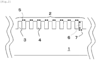
- Fig. 2 is a schematic cross-sectional view of the wafer 1 showing a part of the a-a' cross-section in Fig. 1 .
- Fig. 3 is a diagram showing a step of supplying a vapor 9 of the composition to concave portions 4 holding a liquid 8.
- Fig. 4 is a diagram showing a step of cleaning the concave portion 4, in which a water-repellent protective film 11 is formed by the composition, using a liquid 10.
- the wafer 1 having an uneven pattern on the surface is prepared.
- the following method which is an example of a method for forming the uneven pattern 2 on the wafer surface, may be used.
- the resist is exposed to light through a resist mask and either the exposed resist or the unexposed resist is removed to produce a resist having a desired uneven pattern.
- it is possible to obtain a resist having an uneven pattern by pressing a mold having a pattern against the resist.
- the wafer is etched.
- the substrate surface corresponding to the concave portions of the resist pattern is selectively etched.
- the wafer 1 having the uneven pattern 2 on the surface is obtained.
- the materials of the wafer on which the uneven pattern 2 is formed and the uneven pattern 2 are not particularly limited.
- wafers such as silicon wafers, silicon carbide wafers, wafers composed of a plurality of components including a silicon element, sapphire wafers, and various compound semiconductor wafers.
- the material of the uneven pattern 2 may include one or two or more selected from the group consisting of Si, Ti, Ge, W, and Ru, and oxides, nitrides, nitrogen oxides, carbonitrides, and carbide oxides including one or more of the above.
- the material of the uneven pattern 2 it is possible to use silicon-based materials such as silicon oxide, silicon nitride, polycrystalline silicon, single crystal silicon, and silicon germanium, metal-based materials such as titanium nitride, tungsten, ruthenium, tantalum nitride, and tin, various combinations of the above-described materials, resist (photoresist) materials, and the like.
- the uneven pattern 2 may be formed to have a three-dimensional structure having one or two or more structures arranged along an orthogonal direction to the surface, and/or one or two or more structures arranged along the horizontal direction perpendicular to the orthogonal direction.
- a three-dimensional structure at least a part of a logic device or a memory device may be formed and examples thereof include a FinFET, a nanowire FET, a nanosheet FET, or another multi-gate type FET, three-dimensional memory cells, and the like.
- Fig. 2 is a cross-sectional view showing an example of the uneven pattern 2.
- the pattern dimension of the uneven pattern 2 as at least one dimension in the width direction in the in-plane direction of the surface and/or at least one dimension in the height direction in the direction orthogonal to the surface.
- At least one or more pattern dimension of the width and height or, in a three-dimensional structure (XYZ three-dimensional coordinates) in the pattern of the uneven pattern 2 may be, for example, 30 nm or less, 20 nm or less, or 10 nm or less.
- the above may be the interval between patterns. Even when the wafer 1 having the fine uneven pattern 2 is used, it is possible to apply the surface treatment composition of the present embodiment.
- Such a surface treatment composition is suitable for a surface treatment of, for example, the wafer 1 having the uneven pattern 2 having a pattern dimension of 30 nm or less, preferably 20 nm or less.
- the aspect ratio of convex portions 3 may be, for example, 3 or more, 5 or more, or 10 or more. It is possible to suppress pattern collapse even in the uneven pattern 2 having the convex portions 3 having a fragile structure.
- the aspect ratio of the convex portions 3 is not particularly limited, but may be 100 or less.
- the aspect ratio of the convex portions 3 is expressed as the value obtained by dividing a height 6 of the convex portions by a width 7 of the convex portions.
- a width 5 of the concave portions may be, for example, 70 nm or less, preferably 45 nm or less.
- the width 5 of the concave portions is indicated by the interval between adjacent convex portions 3 in the cross-sectional view of Fig. 2 .
- the surface of the wafer 1 is cleaned with a cleaning liquid.
- the surface of the wafer 1 may be brought into contact with an aqueous cleaning solution that is one of the cleaning liquids.
- aqueous cleaning solutions examples include water, alcohol, ammonium hydroxide aqueous solutions, tetramethylammonium aqueous solutions, hydrofluoric acid aqueous solutions, hydrochloric acid aqueous solutions, hydrogen peroxide aqueous solutions, sulfuric acid aqueous solutions, organic solvents, and the like. The above may be used alone or in a combination of two or more.
- the cleaning step may be performed once or twice or more before the surface treatment step or before the first rinsing step described below. Other steps may be included between the plurality of cleaning steps or between the cleaning step and the surface treatment step.
- the surface of the wafer 1 may be brought into contact with a first rinsing solution, which is one of the cleaning liquids (first rinsing step).
- the first rinsing solution it is possible to use a cleaning liquid different from the aqueous cleaning solution and examples thereof include water, an organic solvent, a mixture thereof, or a cleaning liquid mixed thereof with at least one of an acid, an alkali, a surfactant, and an oxidizing agent, or the like.
- Examples of the organic solvent used in the first rinsing solution include hydrocarbons, esters, ethers, ketones, halogen element-containing solvents, sulfoxide-based solvents, alcohols, polyhydric alcohol derivatives, nitrogen element-containing solvents, and the like.
- the organic solvent it is preferable to use at least one type of alcohol selected from alcohols having 3 or less carbon atoms, such as methanol, 1-propanol, and 2-propanol (isopropanol).
- a plurality of types may be used as the first rinsing solution.
- an aqueous cleaning solution may be added and the rinsing may be performed in the order of a solution including an acid aqueous solution or an alkaline aqueous solution, an aqueous cleaning solution, and an organic solvent.
- the first rinsing step may be performed once or twice or more after the cleaning step or before the surface treatment step. Other steps may be included between the plurality of first rinsing steps or between the first rinsing step and the surface treatment step.
- a known means and examples thereof include a single-wafer system represented by a cleaning method using a spin cleaning device that cleans the wafers one by one by supplying a cleaning liquid near the center of rotation while holding the wafers almost horizontally and rotating and a batch system using a cleaning device that immerses and cleans a plurality of wafers in a cleaning tank.
- the cleaning liquid may be supplied using vapor, as in the surface treatment composition described below.
- the vapor 9 of the surface treatment composition of the present embodiment is supplied to the surface of the uneven pattern, the vapor 9 changes state to become the liquid 10 on the wafer surface, and the liquid 8 held in at least the concave portions 4 is replaced with the liquid 10, which is held to form a water-repellent protective film (the protective film 11) on at least a part of the wafer surface, for example, the surface of the concave portions 4.
- the cleaning liquid (liquid 8) held on the wafer surface may be the above-described aqueous cleaning solution or the first rinsing solution, and, from the viewpoint of production stability, the first rinsing solution is preferable, in which 2-propanol (iPA) may be included. That is, as one aspect of the method for producing a wafer, the vapor 9 of the surface treatment composition may be supplied in a state where iPA is held on the surface of the wafer.
- iPA 2-propanol
- the method for producing a wafer includes a step of mixing the materials of each component of the surface treatment composition, and the total amount of moisture in the materials may be, for example, 2000 ppm by mass or less with respect to the total amount of the materials, preferably 500 ppm by mass or less, more preferably 100 ppm by mass or less, and even more preferably 50 ppm by mass or less.
- the smaller the total amount of moisture in the material the easier it is to obtain a surface treatment composition that easily increases the water contact angle, which is preferable.
- Examples of methods for supplying the vapor 9 of the surface treatment composition include a method in which the wafer 1 holding the liquid 8 in at least the concave portions 4 of the uneven pattern 2 is arranged in a chamber and vapor obtained by separately evaporating the surface treatment composition is supplied to the surface of the uneven pattern via piping or a nozzle, and the like.
- a carrier gas such as nitrogen gas or dry air may be used when supplying the vapor.
- the method for vaporizing the surface treatment composition is not particularly limited to the above-described method.
- Examples thereof include a batch-type vaporization method in which a predetermined amount of a surface treatment composition in a liquid state is introduced into a vaporization chamber, sufficient heating is performed to evaporate the entire amount of the surface treatment composition, and after the entire amount evaporates, the vapor 9 is sent out to piping or a nozzle to be supplied to the surface of the uneven pattern.
- another example is a continuous vaporization method in which droplets of the surface treatment composition are dropped into a small preheated vaporization section (for example, by installing a heating means in a part of the piping) such that the entire amount of the surface treatment composition evaporates with each drop and the vapor 9 is sent out to piping or a nozzle to be supplied to the surface of the uneven pattern.
- the vaporization temperature is preferably suppressed to a temperature at which there is no risk of causing thermal decomposition of the silylating agent, which is a protective film forming component.
- Examples of preferable vapor treatment conditions include introducing nitrogen gas and supplying the mixed gas to the uneven pattern surface after the composition of the mixed gas of the vapor obtained as described above and the nitrogen gas becomes constant.
- the ambient temperature near the substrate during treatment that is, the temperature of the vapor, is preferably lower than the boiling point of the liquid 8 held in the concave portions 4.
- Fig. 3 shows a schematic view of a state in which the vapor 9 is supplied to the concave portions 4 holding the liquid 8.
- Fig. 4 shows a schematic view of the state of the concave portions 4 where the water-repellent protective film 11 is formed using the surface treatment composition.
- the wafer 1 in the schematic views of Fig. 3 and Fig. 4 shows a part of the a-a' cross-section of Fig. 1 .
- the supplied vapor 9 changes state to become the liquid 10 in the concave portions 4, the liquid 8 held in the concave portions 4 is replaced with the liquid 10, and the liquid 10 is held in the concave portions 4.
- the temperature of the wafer 1 and the concave portion 4 may be adjusted by lowering or keeping the temperature constant, or the like.
- the silylating agent of the liquid 10 reacts with the wafer surface and the above-described site having a water-repellent functional group is fixed to the wafer surface to form a water-repellent protective film (the protective film 11).
- the protective film 11 is not necessarily formed continuously or formed uniformly, but is more preferably formed continuously and uniformly since it is possible to provide better water repellency.
- the formation of the protective film 11 may be promoted by applying a known means such as a heating treatment, a reduced pressure treatment, or a drying treatment to the liquid 10 held on the wafer surface.
- the wafer surface on which the protective film 11 is formed may be brought into contact with a second rinsing solution (second rinsing step).
- the second rinsing solution it is possible to use the solutions described as examples for the first rinsing solution.
- a plurality of types may be used as the second rinsing solution.
- the second rinsing step may be performed once or twice or more after the surface treatment step. Other steps may be included between the plurality of second rinsing steps or between the second rinsing step and the surface treatment step.
- a drying step for drying the surface of the wafer 1 may be performed, as necessary.
- the liquid may include the liquid 10, the second rinsing solution, or a mixed liquid thereof.
- a drying means for example, a known means may be used, such as a spin drying method, iPA (2-propanol) vapor drying, Marangoni drying, heat drying, hot air drying, vacuum drying, and reduced pressure drying.
- the drying step may be performed once or twice or more, and may be performed, for example, after the surface treatment step or after the second rinsing step.
- the drying step and the second rinsing step may be alternately repeated.
- the protective film 11 on the surface of the wafer 1 may be removed (removal step).
- removal means include heating, UV irradiation, ozone exposure, plasma irradiation, corona discharge, and the like.
- a treatment using a concentrated fluid such as a supercritical fluid (which may include an acid, a base, and an oxidizing agent) or a vapor treatment may be performed.
- a supercritical fluid which may include an acid, a base, and an oxidizing agent
- a vapor treatment may be performed. The above may be used alone or in a combination of two or more. These treatments may be performed under atmospheric pressure or reduced pressure.
- the wafer 1 (semiconductor substrate) using the surface treatment composition of the present embodiment is obtained.
- the present invention is not limited thereto.
- the substrate production method of the present embodiment with the resist pattern as the target, it is also possible to suppress collapse of the resist pattern by using the surface treatment composition of the present invention in the cleaning and drying steps.
- the supply step is not limited thereto and may be carried out after various treatments carried out on the uneven pattern 2.
- the substrate production method may use one or a combination of two or more known treatments.
- a surface treatment such as a plasma treatment may be performed.
- the present invention is not limited only to these Examples.
- composition 5 g of trimethylsilyldimethylamine [(CH 3 ) 3 Si-N(CH 3 ) 2 ] (referred to below as “TMSDMA”) as a silylating agent and 95 g of tert-butylbenzene as a solvent were mixed to obtain a surface treatment composition (referred to below as “composition").
- TMSDMA trimethylsilyldimethylamine
- the vapor of the above-described composition was supplied to a wafer having a smooth surface to form a protective film on the wafer surface, this protective film was regarded as a protective film formed on the surface of a wafer having an uneven pattern on the surface, and the following procedure was used for evaluation.
- a silicon wafer to which a thermal oxide film was attached and which had a SiO 2 layer on a silicon wafer having a smooth surface was used as the wafer having a smooth surface.
- a smooth silicon wafer to which a thermal oxide film was attached (Si wafer having a 1 ⁇ m thick thermal oxide film layer on the surface; manufactured by Kyodo International, Inc.) which was 2 cm square in size was immersed in a 1% by mass hydrofluoric acid aqueous solution at 25°C for 10 minutes, immersed at 25°C for 1 minute in pure water, and then immersed at 25°C for 1 minute in 2-propanol (referred to below as "iPA").
- the silicon wafer is arranged horizontally in a vapor treatment chamber in a state of being filled to the brim with iPA and the composition in the solution state prepared as described above was vaporized under the vapor supply conditions described below and the vapor is supplied to the vapor treatment chamber.
- the supplied vapor was changed to a liquid state on the wafer surface at a temperature of 50°C or lower and the iPA held on the wafer surface was replaced with the liquid.
- Vapor supply conditions for the above-described composition while nitrogen gas flowed at a rate of 2 dm 3 /min, the above-described prepared composition in a solution state was dropped at a drop rate of 0.01 g/sec into the vaporization chamber heated to 165°C and the entire drop amount was vaporized. The vapor was immediately supplied to the vapor treatment chamber using the nitrogen gas flow. This treatment was performed for 40 seconds.
- the silicon wafer was taken out of the vapor treatment chamber and immersed in iPA at 25°C for 1 minute. Finally, the silicon wafer was taken out from the iPA and the iPA on the surface was removed by blowing air.
- Table 1 Composition Boiling point difference between silylating agent and solvent [°C] Evaluation Silylating agent Solvent Content of hydrocarbon solvent in solvent [% by mass] Content of silylating agent in a total amount of composition [% by mass] Water contact angle (average value) [°] Variation in water contact angle (standard deviation)
- Example 1 TMSDMA tert-butylbenzene 100 5 101 87 0.9
- Example 2 TMSDMA 1,3,5-trimethylbenzene 100 5 79 87 0.5
- Example 3 TMSDMA 1,2,4-trimethylbenzene 100 5 83 87 0.5
- Example 4 PDMSDMA 1,2,4-trimethylbenzene 100 5 91 0.6
- Example 5 BDMSDMA 1,2,4-trimethylbenzene 100 5 91 0.6
- Example 6 PDMSDMA 1,2,4-trimethylbenzene 100 3 90 0.6
- Example 7 BDMSDMA 1,2,4-trimethylbenzene 100 10 92 0.5
- Example 8 TMSDMA
- compositions were prepared in the same manner as in Example 1, except that the solvents listed in Table 1 were used as the solvent, various evaluations were performed, and the results are shown in Table 1.
- Table 1 the value of the boiling point difference between the silylating agent and the solvent is calculated using known reference values or catalog values and "-" indicates that the value is not calculated due to the absence of a reference value or the like.
- "-" in the water contact angle variation indicates that measurement was not carried out.
- the solvent in Example 24 is a mixed solvent of 60% by mass of 1,2,4-trimethylbenzene and 40% by mass of isododecane in the total amount of the solvent
- the solvent in Example 25 is a mixed solvent of 60% by mass of 1,3,5-trimethylbenzene and 40% by mass of isododecane
- the solvent in Example 26 is a mixed solvent of 60% by mass of tert-butylbenzene and 40% by mass of isododecane
- the solvent in Example 27 is a mixed solvent of 98% by mass of 1,2,4-trimethylbenzene and 2% by mass of propylene glycol monoethyl ether acetate (PGMEA)
- the solvent in Example 28 is a mixed solvent of 80% by mass of 1,2,4-trimethylbenzene and 20% by mass of PGMEA
- the solvent in Example 29 is a mixed solvent of 98% by mass of tert-butylbenzene and 2% by mass of PGMEA
- the solvent in Example 30
- the solvent of Comparative Example 1 is a mixed solvent of 47% by mass of propylene carbonate and 53% by mass of diethyl carbonate in the total amount of the solvent and the solvent of Comparative Example 2 is a mixed solvent of 70% by mass of 1,2,4-trimethylbenzene and 30% by mass of PGMEA in the total amount of the solvent.
- silylating agent in Example 4 and Example 6 is propyldimethylsilyldimethylamine [PDMSDMA: (CH 3 CH 2 CH 2 )(CH 3 ) 2 Si-N(CH 3 ) 2 ] and the silylating agent in Example 5 and Example 6 is butyldimethylsilyldimethylamine [BDMSDMA: (CH 3 CH 2 CH 2 CH 2 )(CH 3 ) 2 Si-N(CH 3 ) 2 ].
- the surface treatment composition of the present invention may be said to easily increase the water contact angle in comparison with the related art.
Landscapes
- Chemical & Material Sciences (AREA)
- Life Sciences & Earth Sciences (AREA)
- Engineering & Computer Science (AREA)
- Materials Engineering (AREA)
- Wood Science & Technology (AREA)
- Organic Chemistry (AREA)
- Cleaning Or Drying Semiconductors (AREA)
- Materials Applied To Surfaces To Minimize Adherence Of Mist Or Water (AREA)
Applications Claiming Priority (3)
| Application Number | Priority Date | Filing Date | Title |
|---|---|---|---|
| JP2022065098 | 2022-04-11 | ||
| JP2022128657 | 2022-08-12 | ||
| PCT/JP2023/014102 WO2023199824A1 (ja) | 2022-04-11 | 2023-04-05 | 表面処理組成物、およびウェハの製造方法 |
Publications (1)
| Publication Number | Publication Date |
|---|---|
| EP4510171A1 true EP4510171A1 (en) | 2025-02-19 |
Family
ID=88329634
Family Applications (1)
| Application Number | Title | Priority Date | Filing Date |
|---|---|---|---|
| EP23788243.6A Withdrawn EP4510171A1 (en) | 2022-04-11 | 2023-04-05 | Surface treatment composition and method for producing wafer |
Country Status (6)
| Country | Link |
|---|---|
| US (1) | US20250210375A1 (https=) |
| EP (1) | EP4510171A1 (https=) |
| JP (1) | JPWO2023199824A1 (https=) |
| KR (1) | KR20240151193A (https=) |
| TW (1) | TW202347482A (https=) |
| WO (1) | WO2023199824A1 (https=) |
Family Cites Families (13)
| Publication number | Priority date | Publication date | Assignee | Title |
|---|---|---|---|---|
| US9244358B2 (en) * | 2008-10-21 | 2016-01-26 | Tokyo Ohka Kogyo Co., Ltd. | Surface treatment liquid, surface treatment method, hydrophobilization method, and hydrophobilized substrate |
| JP5482192B2 (ja) * | 2009-01-21 | 2014-04-23 | セントラル硝子株式会社 | シリコンウェハ用洗浄剤 |
| JP5648053B2 (ja) * | 2010-06-30 | 2015-01-07 | セントラル硝子株式会社 | ウェハパターンの保護膜形成用薬液、薬液の調製方法およびウェハ処理方法 |
| CN112951250B (zh) | 2014-09-12 | 2025-02-07 | 索尼公司 | 发送装置、发送方法、接收装置以及接收方法 |
| JP6703256B2 (ja) * | 2016-03-15 | 2020-06-03 | セントラル硝子株式会社 | 撥水性保護膜形成剤、撥水性保護膜形成用薬液、及びウェハの洗浄方法 |
| JP6963166B2 (ja) * | 2017-04-17 | 2021-11-05 | セントラル硝子株式会社 | ウェハの表面処理方法及び該方法に用いる組成物 |
| JP2019080009A (ja) * | 2017-10-27 | 2019-05-23 | セントラル硝子株式会社 | ウェハの洗浄方法 |
| JP7277700B2 (ja) * | 2018-01-15 | 2023-05-19 | セントラル硝子株式会社 | 撥水性保護膜形成用薬液、及びウェハの表面処理方法 |
| CN111699546B (zh) * | 2018-02-13 | 2023-09-12 | 中央硝子株式会社 | 拒水性保护膜形成剂和拒水性保护膜形成用化学溶液 |
| SG11202009171XA (en) | 2018-04-05 | 2020-10-29 | Central Glass Co Ltd | Surface treatment method of wafer and composition used for said method |
| JP7292020B2 (ja) * | 2018-08-27 | 2023-06-16 | 東京応化工業株式会社 | 表面処理剤及び表面処理方法 |
| JP2022128657A (ja) | 2021-02-24 | 2022-09-05 | トヨタ自動車東日本株式会社 | ワイパーモジュール |
| KR20230093311A (ko) * | 2021-02-26 | 2023-06-27 | 샌트랄 글래스 컴퍼니 리미티드 | 표면 처리 조성물, 및 웨이퍼의 제조 방법 |
-
2023
- 2023-04-05 US US18/845,594 patent/US20250210375A1/en active Pending
- 2023-04-05 JP JP2024514922A patent/JPWO2023199824A1/ja active Pending
- 2023-04-05 KR KR1020247030369A patent/KR20240151193A/ko not_active Withdrawn
- 2023-04-05 WO PCT/JP2023/014102 patent/WO2023199824A1/ja not_active Ceased
- 2023-04-05 EP EP23788243.6A patent/EP4510171A1/en not_active Withdrawn
- 2023-04-07 TW TW112113142A patent/TW202347482A/zh unknown
Also Published As
| Publication number | Publication date |
|---|---|
| US20250210375A1 (en) | 2025-06-26 |
| TW202347482A (zh) | 2023-12-01 |
| WO2023199824A1 (ja) | 2023-10-19 |
| KR20240151193A (ko) | 2024-10-17 |
| JPWO2023199824A1 (https=) | 2023-10-19 |
Similar Documents
| Publication | Publication Date | Title |
|---|---|---|
| US9748092B2 (en) | Liquid chemical for forming protecting film | |
| JP6032338B2 (ja) | 保護膜形成用薬液 | |
| US8828144B2 (en) | Process for cleaning wafers | |
| CN107068540A (zh) | 晶片的清洗方法 | |
| CN111886676B (zh) | 晶圆的表面处理方法及用于该方法的组合物 | |
| US12588446B2 (en) | Surface treatment composition and method for producing wafer | |
| JP2012033880A (ja) | 撥水性保護膜形成用薬液 | |
| JP5716527B2 (ja) | 撥水性保護膜形成用薬液と該薬液を用いたウェハの洗浄方法 | |
| EP4459666A1 (en) | Composition for film formation and method for producing substrate | |
| EP4510171A1 (en) | Surface treatment composition and method for producing wafer | |
| EP4155376A1 (en) | Surface treatment method for semiconductor substrate, and surface treatment agent composition | |
| CN118974894A (zh) | 表面处理组合物及晶圆的制造方法 | |
| US11282709B2 (en) | Chemical agent for forming water repellent protective film and surface treatment method for wafers | |
| JP6098741B2 (ja) | ウェハの洗浄方法 | |
| WO2012002243A1 (ja) | 撥水性保護膜形成剤、撥水性保護膜形成用薬液と該薬液を用いたウェハの洗浄方法 | |
| TW202512261A (zh) | 基材的處理方法及基材的製造方法 | |
| WO2026063320A1 (ja) | ウェハの製造方法、加熱蒸散用の表面処理組成物、表面処理組成物の使用方法、蒸気組成物および蒸気組成物の製造方法 | |
| JP5712670B2 (ja) | 撥水性保護膜形成薬液 | |
| CN121153104A (zh) | 膜形成用组合物、基板的制造方法及膜形成用组合物的制造方法 |
Legal Events
| Date | Code | Title | Description |
|---|---|---|---|
| STAA | Information on the status of an ep patent application or granted ep patent |
Free format text: STATUS: THE INTERNATIONAL PUBLICATION HAS BEEN MADE |
|
| PUAI | Public reference made under article 153(3) epc to a published international application that has entered the european phase |
Free format text: ORIGINAL CODE: 0009012 |
|
| STAA | Information on the status of an ep patent application or granted ep patent |
Free format text: STATUS: REQUEST FOR EXAMINATION WAS MADE |
|
| 17P | Request for examination filed |
Effective date: 20240902 |
|
| AK | Designated contracting states |
Kind code of ref document: A1 Designated state(s): AL AT BE BG CH CY CZ DE DK EE ES FI FR GB GR HR HU IE IS IT LI LT LU LV MC ME MK MT NL NO PL PT RO RS SE SI SK SM TR |
|
| STAA | Information on the status of an ep patent application or granted ep patent |
Free format text: STATUS: THE APPLICATION HAS BEEN WITHDRAWN |
|
| 18W | Application withdrawn |
Effective date: 20250331 |