EP4409576B1 - Verfahren zur bestimmung defekter chips mit nichtflüchtigen speicherzellen - Google Patents
Verfahren zur bestimmung defekter chips mit nichtflüchtigen speicherzellen Download PDFInfo
- Publication number
- EP4409576B1 EP4409576B1 EP22703192.9A EP22703192A EP4409576B1 EP 4409576 B1 EP4409576 B1 EP 4409576B1 EP 22703192 A EP22703192 A EP 22703192A EP 4409576 B1 EP4409576 B1 EP 4409576B1
- Authority
- EP
- European Patent Office
- Prior art keywords
- memory cells
- die
- volatile memory
- threshold voltage
- predetermined
- Prior art date
- Legal status (The legal status is an assumption and is not a legal conclusion. Google has not performed a legal analysis and makes no representation as to the accuracy of the status listed.)
- Active
Links
Images



Classifications
-
- G—PHYSICS
- G11—INFORMATION STORAGE
- G11C—STATIC STORES
- G11C29/00—Checking stores for correct operation ; Subsequent repair; Testing stores during standby or offline operation
- G11C29/04—Detection or location of defective memory elements, e.g. cell constructio details, timing of test signals
- G11C29/08—Functional testing, e.g. testing during refresh, power-on self testing [POST] or distributed testing
- G11C29/12—Built-in arrangements for testing, e.g. built-in self testing [BIST] or interconnection details
- G11C29/44—Indication or identification of errors, e.g. for repair
-
- G—PHYSICS
- G11—INFORMATION STORAGE
- G11C—STATIC STORES
- G11C29/00—Checking stores for correct operation ; Subsequent repair; Testing stores during standby or offline operation
- G11C29/04—Detection or location of defective memory elements, e.g. cell constructio details, timing of test signals
- G11C29/50—Marginal testing, e.g. race, voltage or current testing
- G11C29/50004—Marginal testing, e.g. race, voltage or current testing of threshold voltage
-
- G—PHYSICS
- G11—INFORMATION STORAGE
- G11C—STATIC STORES
- G11C29/00—Checking stores for correct operation ; Subsequent repair; Testing stores during standby or offline operation
- G11C29/04—Detection or location of defective memory elements, e.g. cell constructio details, timing of test signals
- G11C29/50—Marginal testing, e.g. race, voltage or current testing
- G11C29/50016—Marginal testing, e.g. race, voltage or current testing of retention
-
- G—PHYSICS
- G11—INFORMATION STORAGE
- G11C—STATIC STORES
- G11C29/00—Checking stores for correct operation ; Subsequent repair; Testing stores during standby or offline operation
- G11C29/04—Detection or location of defective memory elements, e.g. cell constructio details, timing of test signals
- G11C2029/0403—Detection or location of defective memory elements, e.g. cell constructio details, timing of test signals during or with feedback to manufacture
-
- G—PHYSICS
- G11—INFORMATION STORAGE
- G11C—STATIC STORES
- G11C29/00—Checking stores for correct operation ; Subsequent repair; Testing stores during standby or offline operation
- G11C29/04—Detection or location of defective memory elements, e.g. cell constructio details, timing of test signals
- G11C2029/0405—Detection or location of defective memory elements, e.g. cell constructio details, timing of test signals comprising complete test loop
-
- G—PHYSICS
- G11—INFORMATION STORAGE
- G11C—STATIC STORES
- G11C29/00—Checking stores for correct operation ; Subsequent repair; Testing stores during standby or offline operation
- G11C29/04—Detection or location of defective memory elements, e.g. cell constructio details, timing of test signals
- G11C29/50—Marginal testing, e.g. race, voltage or current testing
- G11C2029/5002—Characteristic
-
- G—PHYSICS
- G11—INFORMATION STORAGE
- G11C—STATIC STORES
- G11C29/00—Checking stores for correct operation ; Subsequent repair; Testing stores during standby or offline operation
- G11C29/04—Detection or location of defective memory elements, e.g. cell constructio details, timing of test signals
- G11C29/50—Marginal testing, e.g. race, voltage or current testing
- G11C2029/5006—Current
-
- G—PHYSICS
- G11—INFORMATION STORAGE
- G11C—STATIC STORES
- G11C29/00—Checking stores for correct operation ; Subsequent repair; Testing stores during standby or offline operation
- G11C29/04—Detection or location of defective memory elements, e.g. cell constructio details, timing of test signals
- G11C29/06—Acceleration testing
Definitions
- the present invention relates to memory devices, and more particularly to non-volatile memory devices.
- Non-volatile memory devices having memory cells each with a floating gate disposed over and insulated from a channel region of a semiconductor substrate are known.
- the charge on the floating gate controls the conductivity of the channel region during a read operation.
- To program the memory cell electrons are placed in the floating gate during a program operation.
- To erase the memory cell the electrons are removed from the floating gate during an erase operation.
- the program state of the memory cell is dictated by the charge (i.e., number of electrons) on the floating gate, which is measured during a read operation by detecting the level of current (referred to as the read current) through the channel region when the appropriate read voltages are applied to the memory cell.
- the higher the program state of the memory cell i.e., the greater number of electrons on the floating gate
- the lower the program state i.e., the fewer number of electrons on the floating gate
- the program state of the memory cell can be set to store data. For example, a high program state can reflect a "0" bit value, and a low program state can reflect a "1" bit value.
- the memory cell can also be operated in analog mode where any number of program states can be used to store data.
- a high temperature bake can be referred to as a data retention bake
- One challenge with the read test can be determining the proper predetermined read current threshold for the read test, and how best to apply it. Even with a die containing only good memory cells, there still will be a range of read current values for the good memory cells, not just a single read current value. Moreover, during a data retention bake, all memory cells on a die may experience some minor decrease of read current. However, defective memory cells may experience a larger read current drop compared to normal memory cells. The challenge is reliably detecting the presence of these defective cells, whose read currents deviate from the normal range of read currents exhibited by the good memory cells. If the predetermined read current threshold is set too high, then dies with only good memory cells can be erroneously determined to be defective.
- the predetermined read current threshold is set too low, then dies with defective memory cells can be erroneously determined to be not defective. Another issue is that the range of read current values for good memory cells can vary from die to die. Therefore, an ideal predetermined read current threshold for one die can be less accurate for another die in reliably determining which dies are good and which are defective.
- US 20130114337 A1 discloses a method of decreasing the test time to determine data retention (e.g. leakage current) of a memory cell having a floating gate for the storage of charges thereon.
- the memory cell is characterized by the leakage current having a rate of leakage which is dependent upon the absolute value of the voltage of the floating gate.
- the memory cell is further characterized by a first erase voltage and a first programming voltage, applied during normal operation, and a first read current detected during normal operation.
- the method applies a voltage greater than the first erase voltage or greater than the first programming voltage, to over erase the floating gate.
- the memory cell including the floating gate is subject to a single high temperature bake. The memory cell is then tested for data retention of the floating gate based on the single high temperature bake.
- US 20210192333 A1 discloses a system comprising a memory component having a plurality of memory cells capable of being in a plurality of states, each state of the plurality of states corresponding to a value stored by the memory cell, and a processing device, operatively coupled with the memory component, to perform operations comprising: obtaining, for the plurality of memory cells, a plurality of distributions of threshold voltages, wherein each of the plurality of distributions corresponds to one of the plurality of states, classifying each of the plurality of distributions among one of a plurality of classes, generating a vector comprising a plurality of components, wherein each of the plurality of components represents the class of a respective one of the plurality of distributions, and processing, using a classifier, the generated vector to determine a likelihood that the memory component will fail within a target period of time.
- US 20060120165 A1 discloses a program voltage signal implemented as a series of increasing program voltage pulses is applied to a set of non-volatile storage elements. Different increment values can be used when programming memory cells to different memory states. A smaller increment value can be used when programming memory cells to lower threshold voltage memory states and a larger increment value used when programming memory cells to higher threshold voltage memory states such as the highest memory state in an implementation.
- non-volatile storage elements of a set are programmed to different memory states under simultaneous application of a single program voltage signal, programming can be monitored to determine when lower state programming is complete. The increment value can then be increased to complete programming to the highest memory state. Coarse/fine programming methodology can be incorporated for the highest memory state when the increment value is increased to maintain the threshold distribution within a reasonable range.
- US 20200160933 A1 discloses that a testing method is provided for testing a memory die of a non-volatile memory.
- the testing method includes the following steps. Firstly, an erase action is performed on plural memory cells of the memory die. Then, a stress is applied to the plural memory cells of the memory die. Then, a read action is performed on the plural memory cells of the memory die to have the plural memory cells generate plural off currents, and a maximum off current is acquired from the plural off currents. Then, a specified test criterion set is selected from plural test criterion sets according to the maximum off current, and the memory die is tested according to plural test currents or plural test voltages of the specified test criterion set.
- a method of testing non-volatile memory cells having floating gates and formed on a die that includes erasing the non-volatile memory cells, performing a first read operation after the erasing of the non-volatile memory cells to determine a lowest read current RC1 for the non-volatile memory cells and a first number N1 of the non-volatile memory cells having the lowest read current RC1, performing a second read operation to determine a second number N2 of the non-volatile memory cells having a read current not exceeding a target read current RC2, wherein the target read current RC2 is equal to the lowest read current RC1 plus a predetermined current value, determining whether the second number N2 exceeds the first number N1 plus a predetermined number, and determining the die is acceptable if the second number N2 is determined to exceed the first number N1 plus the predetermined number, or determining the die is defective if the second number N2 is determined not to exceed the first number N1 plus the predetermined number
- a method of testing non-volatile memory cells having floating gates and formed on a die that includes erasing the non-volatile memory cells, performing a first read operation after the erasing of the non-volatile memory cells to determine a highest threshold voltage TV1 for the non-volatile memory cells and a first number N1 of the non-volatile memory cells having the highest threshold voltage TV1, performing a second read operation to determine a second number N2 of the non-volatile memory cells having a threshold voltage not below a target threshold voltage TV2, wherein the target threshold voltage TV2 is equal to the highest threshold voltage TV1 minus a predetermined voltage value, determining whether the second number N2 exceeds the first number N1 plus a predetermined number, and determining the die is acceptable if the second number N2 is determined to exceed the first number N1 plus the predetermined number, or determining the die is defective if the second number N2 is determined not to exceed the first number N1 plus the predetermined number.
- a method of testing non-volatile memory cells having floating gates and formed on a die that includes programming the non-volatile memory cells, performing a first read operation after the programming of the non-volatile memory cells to determine a lowest threshold voltage TV3 for the non-volatile memory cells and a first number N1 of the non-volatile memory cells having the lowest threshold voltage TV3, performing a second read operation to determine a second number N2 of the non-volatile memory cells having a threshold voltage not exceeding a target threshold voltage TV4, wherein the target threshold voltage TV4 is equal to the lowest threshold voltage TV3 plus a predetermined voltage value, determining whether the second number N2 exceeds the first number N1 plus a predetermined number, and determining the die is acceptable if the second number N2 is determined to exceed the first number N1 plus the predetermined number, or determining the die is defective if the second number N2 is determined not to exceed the first number N1 plus the predetermined number.
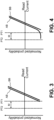
- Fig. 1 illustrates the normalized probability of read current for the memory cells in a die that contains only good memory cells, both before a data retention bake operation on the die (shown by line BB for before-bake) and after the bake operation on the die (shown by line AB for after-bake).
- each point on the normalized distribution represents the cumulative number of memory cells exhibiting a read current at or below the corresponding read current value. The present inventors discovered that such a distribution is normal (linear in the normalized probability scale) if all the memory cells are good, but that defective cells may deviate from that linear distribution.
- the bake operation tends to lower the read current of the erased memory cells.
- Fig. 2 illustrates the normalized probability of read current for the memory cells on a die that contains some defective memory cells.
- the before bake normalized distribution does not include read current values that deviate from the linear distribution of normalized probability of read current, that is not the case for the after bake normalized distribution, which shows memory cells with read currents well below the rest of the memory cells that exhibit the linear distribution of normalized probability of read current.
- the distribution of normalized probability of read current includes a tail portion that deviates significantly from the linear portion of the distribution, which is indicative of defective memory cells that warrant finding the die defective. It should be noted that a tail portion could exist in the prebake normalized probability of read current as well, also indicative of defective memory cells and therefore a defective die.
- Fig. 3 illustrates the normalized probability of read current for the memory cells in a die that contains only good memory cells, with two example predetermined read current thresholds for the read current testing.
- Predetermined threshold PT1 represents no margin, meaning one or more memory cells represented by the lower end of the normalized probability of read current have a read current that does not meet the predetermined threshold PT1.
- Using the predetermined threshold PT1 runs the risk that the die is deemed defective when in fact it should not be deemed defective, since the distribution is linear.
- Predetermined threshold PT2 represents a margin M, meaning all memory cells do meet the predetermined threshold PT2 (and in fact exceed the predetermined threshold PT2 by an amount of margin M), so that the die is properly deemed not defective.
- Using a predetermined threshold PT2 with margin M can be advantageous because the normalized probability distributions can shift somewhat from die to die, so a margin M for the predetermined threshold could avoid falsely determining a die to be defective.
- using a margin M may mean a defective die is not properly identified as defective because some of the defective memory cells still have a read current above the predetermined threshold PT2, as illustrated in Fig.
- the solution is the read test technique shown in Fig. 5 , and illustrated in Figs. 6 and 7 .
- the present inventors discovered that more accurate test results can be achieved by detecting outlier cell read currents rather than read currents falling below a predetermined read current threshold.
- the technique is described with respect to distribution D, which corresponds to the distribution of normalized probability BB in Figs. 1-4 if the read test is performed before the bake operation, or which corresponds to the distribution of normalized probability AB in Figs. 1-4 if the read test is performed after the bake operation.
- the read test of Fig. 5 can be, but need not be, performed twice, once before the bake operation and again after the bake operation.
- Step 1 the memory cells in the die are erased using an erase operation (i.e., a conventional erase operation well known in the art).
- Step 2 a bake operation or electrical stress is performed.
- a non-limiting example of a bake operation can include subjecting the wafer containing the die to 250 degrees Celsius for a period of three days.
- a non-limiting example of an electrical stress is the application of one or more voltages to certain gates or the source/drains regions of the memory cells.
- Step 2 is labeled "OPT" for optional, because as described above, the read test can be performed before and/or after the bake operation or electrical stress, or even without a bake operation or electrical stress.
- Step 3 a first read operation is performed to determine the lowest read current RC1 for all the memory cells being tested (e.g., preferably all the memory cells on the die, but a subset of the memory cells on the die can be tested at any given time as well), and a first number N1 of memory cells having that lowest read current RC1.
- An example distribution D of normalized probability of read current for a die with only good memory cells is shown in Fig. 6 .
- An example distribution D for a die with some defective memory cells is shown in Fig. 7 .
- RC1 can be found using a binary search or other search algorithm for all the memory cells being tested.
- the value ⁇ RC is a predetermined current value, and can be selected so that the target read current RC2 corresponds to read current for memory cells in a main portion of the distribution D (i.e., ⁇ RC represents a sufficient detectable gap between the memory cells at the tail portion of the distribution of a defective die and the edge of the main portion (e.g., linear portion) of distribution D, so that the defective memory cells can be detected).
- Step 5 it is determined whether the second number N2 exceeds the first number N1 plus ⁇ N, where ⁇ N is a predetermined number. If the determination is yes, that the second number N2 exceeds N1 + ⁇ N, then it is concluded that the die contains no outlier cells, and the die containing the memory cells is determined to be acceptable. Conversely, if the determination is no, that the second number N2 does not exceed N1 + ⁇ N, then the die containing the memory cells is determined to be defective.
- ⁇ N can be selected such that if there is a tail in the distribution D, then the die will be determined to be defective because the second number N2 would not exceed N1 + ⁇ N (i.e., would be less than or equal to N1 + ⁇ N).
- the die will be determined to be acceptable because the second number N2 would exceed N1 + ⁇ N.
- This determination is graphically shown in Figs. 6 and 7 . Specifically, in Fig. 6 , the second number N2 exceeds N1 + ⁇ N. Therefore, the die represented in Fig. 6 is determined to be acceptable and not defective. In Fig. 7 , the second number N2 does not exceed N1 + ⁇ N. Therefore, the die represented in Fig. 7 is determined to be defective and not acceptable.
- the above described technique applied on a die by die basis, more accurately identifies defective die compared to using a fixed predetermined read current threshold, because it better detects the presence of a small number of read currents for one or a few memory cells that deviate from the general distribution of read currents for the rest of the memory cells (i.e., better detects outlier read currents characteristic of defective memory cells and die).
- the technique also accommodates variations in the distribution of read currents that can vary die to die.
- the values of ⁇ RC and ⁇ N can be chosen based on the properties of the distribution D. As a non-limiting example, ⁇ RC can be with a range of 4-5 ⁇ A, and ⁇ N can be a low number such as within a range of 1-3.
- the above described technique can be implemented on memory cells before the bake operation or electrical stress, after them, or both.
- the bake operation or electrical stress could be performed before the erase operation (i.e., before Step 1 of Fig. 5 ) or could be performed after the erase operation (Step 1) but before the first read operation (Step 3) in Fig. 5 .
- Threshold voltage is the minimum voltage applied to one of the gates of a memory cell (other than the floating gate) such that the channel region is sufficiently conductive to consider the memory cell turned on. Threshold voltage can be determined by ramping up the applied voltage during a read operation until the read current reaches a predetermined read current. When the read current reaches the predetermined read current, the applied voltage at that point is the memory cell's threshold voltage.
- threshold voltage instead of read current is illustrated in Fig. 8 , and shown in Fig. 9 (with distribution D of normalized probability of threshold voltage for a die with only good memory cells) and Fig.
- Step 6 The memory cells in the die are erased using an erase operation (Step 6).
- Step 7 an optional bake operation or electrical stress is performed.
- Step 8 a first read operation is performed to determine the highest threshold voltage TV1 for all the memory cells being tested, and a first number N1 of the memory cells having that highest threshold voltage TV1.
- the value ⁇ TV is a predetermined voltage value, and can be selected so that the target threshold voltage TV2 corresponds to threshold voltage for memory cells in a main portion of the distribution D.
- Step 10 it is determined whether the second number N2 exceeds the first number N1 plus ⁇ N, where ⁇ N is a predetermined number. If the determination is yes, that the second number N2 exceeds N1 + ⁇ N, then the die containing the memory cells is determined to be acceptable. Conversely, if the determination is no, that the second number N2 does not exceed N1 + ⁇ N, then the die containing the memory cells is determined to be defective.
- ⁇ TV can be within a range of 0.5-1.0 V
- ⁇ N can be a low number such as within a range of 1-3.
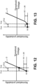
- Fig. 11 Using programmed memory cells and threshold voltage is illustrated in Fig. 11 , and shown in Fig. 12 (with distribution D of normalized probability of threshold voltage for a die with only good memory cells) and Fig. 13 (with distribution D of normalized probability of threshold voltage for a die with some defective memory cells ).
- Step 11 the memory cells in the die are programmed using a program operation (i.e., a conventional program operation well known in the art).
- Programming memory cells can include applying one or more pulses of voltages to each memory cell to place electrons on the floating gate.
- Step 12 an optional bake operation or electrical stress is performed.
- Step 13 a first read operation is performed to determine the lowest threshold voltage TV3 for all the memory cells being tested, and a first number N1 of the memory cells having that lowest threshold voltage TV3.
- the value ⁇ TV2 is a predetermined voltage value, and can be selected so that the target threshold voltage TV4 corresponds to threshold voltage for memory cells in a main portion of the distribution D.
- Step 15 it is determined whether the second number N2 exceeds the first number N1 plus ⁇ N, where ⁇ N is a predetermined number.
- ⁇ TV2 can be within a range of 0.5-1.0 V, and ⁇ N can be a low number such as within a range of 1-3.
Landscapes
- For Increasing The Reliability Of Semiconductor Memories (AREA)
- Read Only Memory (AREA)
- Tests Of Electronic Circuits (AREA)
Claims (15)
- Verfahren zum Testen nichtflüchtiger Speicherzellen, die Floating Gates aufweisen und die auf einem Chip ausgebildet sind, umfassend:Löschen der nichtflüchtigen Speicherzellen;Durchführen eines ersten Lesevorgangs nach dem Löschen der nichtflüchtigen Speicherzellen, um einen niedrigsten Lesestrom (RC1) für die nichtflüchtigen Speicherzellen und eine erste Anzahl (N1) der nichtflüchtigen Speicherzellen, die den niedrigsten Lesestrom (RC1) aufweisen, zu bestimmen;Durchführen eines zweiten Lesevorgangs, um eine zweite Anzahl (N2) der nichtflüchtigen Speicherzellen, die einen Lesestrom aufweisen, der einen Ziellesestrom (RC2) nicht überschreitet, zu bestimmen, wobei der Ziellesestrom (RC2) gleich dem niedrigsten Lesestrom (RC1) plus einem zuvor bestimmten Stromwert ist;Bestimmen, ob die zweite Anzahl (N2) die erste Anzahl (N1) plus eine zuvor bestimmte Anzahl überschreitet; undBestimmen, dass der Chip annehmbar ist, wenn bestimmt wird, dass die zweite Anzahl (N2) die erste Anzahl (N1) plus die zuvor bestimmte Anzahl überschreitet, oder Bestimmen, dass der Chip defekt ist, wenn bestimmt wird, dass die zweite Anzahl (N2) die erste Anzahl (N1) plus die zuvor bestimmte Anzahl nicht überschreitet.
- Verfahren nach Anspruch 1, wobei der zuvor bestimmte Stromwert in einem Bereich von 4-5 µA liegt.
- Verfahren nach Anspruch 1, wobei die zuvor bestimmte Anzahl in einem Bereich von 1-3 liegt.
- Verfahren nach Anspruch 1, ferner umfassend:
Durchführen eines Backvorgangs auf dem Chip vor dem Durchführen des ersten Lesevorgangs. - Verfahren nach Anspruch 1, ferner umfassend:
Durchführen einer elektrischen Belastung der nichtflüchtigen Speicherzellen vor dem Durchführen des ersten Lesevorgangs. - Verfahren zum Testen nichtflüchtiger Speicherzellen, die Floating Gates aufweisen und die auf einem Chip ausgebildet sind, umfassend:Löschen der nichtflüchtigen Speicherzellen;Durchführen eines ersten Lesevorgangs nach dem Löschen der nichtflüchtigen Speicherzellen, um eine höchste Schwellenspannung (TV1) für die nichtflüchtigen Speicherzellen und eine erste Anzahl N1 der nichtflüchtigen Speicherzellen, die die höchste Schwellenspannung (TV1) aufweisen, zu bestimmen;Durchführen eines zweiten Lesevorgangs, um eine zweite Anzahl (N2) der nichtflüchtigen Speicherzellen, die eine Schwellenspannung nicht unter einer Zielschwellenspannung (TV2) aufweisen, zu bestimmen, wobei die Zielschwellenspannung (TV2) gleich der höchsten Schwellenspannung (TV1) minus einem zuvor bestimmten Spannungswert ist;Bestimmen, ob die zweite Anzahl (N2) die erste Anzahl (N1) plus eine zuvor bestimmte Anzahl überschreitet; undBestimmen, dass der Chip annehmbar ist, wenn bestimmt wird, dass die zweite Anzahl (N2) die erste Anzahl (N1) plus die zuvor bestimmte Anzahl überschreitet, oder Bestimmen, dass der Chip defekt ist, wenn bestimmt wird, dass die zweite Anzahl (N2) die erste Anzahl (N1) plus die zuvor bestimmte Anzahl nicht überschreitet.
- Verfahren nach Anspruch 6, wobei der zuvor bestimmte Spannungswert in einem Bereich von 0,5-1,0 V liegt.
- Verfahren nach Anspruch 6, wobei die zuvor bestimmte Anzahl in einem Bereich von 1-3 liegt.
- Verfahren nach Anspruch 6, ferner umfassend:
Durchführen eines Backvorgangs auf dem Chip vor dem Durchführen des ersten Lesevorgangs. - Verfahren nach Anspruch 6, ferner umfassend:
Durchführen einer elektrischen Belastung der nichtflüchtigen Speicherzellen vor dem Durchführen des ersten Lesevorgangs. - Verfahren zum Testen nichtflüchtiger Speicherzellen, die Floating Gates aufweisen und die auf einem Chip ausgebildet sind, umfassend:Programmieren der nichtflüchtigen Speicherzellen;Durchführen eines ersten Lesevorgangs nach dem Programmieren der nichtflüchtigen Speicherzellen, um eine niedrigste Schwellenspannung (TV3) für die nichtflüchtigen Speicherzellen und eine erste Anzahl (N1) der nichtflüchtigen Speicherzellen, die die niedrigste Schwellenspannung (TV3) aufweisen, zu bestimmen;Durchführen eines zweiten Lesevorgangs, um eine zweite Anzahl (N2) der nichtflüchtigen Speicherzellen, die eine Schwellenspannung aufweisen, die eine Zielschwellenspannung (TV4) nicht überschreitet, zu bestimmen, wobei die Zielschwellenspannung (TV4) gleich der niedrigsten Schwellenspannung (TV3) plus einem zuvor bestimmten Spannungswert ist;Bestimmen, ob die zweite Anzahl (N2) die erste Anzahl (N1) plus eine zuvor bestimmte Anzahl überschreitet; undBestimmen, dass der Chip annehmbar ist, wenn bestimmt wird, dass die zweite Anzahl (N2) die erste Anzahl (N1) plus die zuvor bestimmte Anzahl überschreitet, oder Bestimmen, dass der Chip defekt ist, wenn bestimmt wird, dass die zweite Anzahl (N2) die erste Anzahl (N1) plus die zuvor bestimmte Anzahl nicht überschreitet.
- Verfahren nach Anspruch 11, wobei der zuvor bestimmte Spannungswert in einem Bereich von 0,5-1,0 V ist.
- Verfahren nach Anspruch 11, wobei die zuvor bestimmte Anzahl in einem Bereich von 1-3 ist.
- Verfahren nach Anspruch 11, ferner umfassend:
Durchführen eines Backvorgangs auf dem Chip vor dem Durchführen des ersten Lesevorgangs. - Verfahren nach Anspruch 11, ferner umfassend:
Durchführen einer elektrischen Belastung der nichtflüchtigen Speicherzellen vor dem Durchführen des ersten Lesevorgangs.
Applications Claiming Priority (3)
| Application Number | Priority Date | Filing Date | Title |
|---|---|---|---|
| US202163248964P | 2021-09-27 | 2021-09-27 | |
| US17/576,754 US12020762B2 (en) | 2021-09-27 | 2022-01-14 | Method of determining defective die containing non-volatile memory cells |
| PCT/US2022/012710 WO2023048755A1 (en) | 2021-09-27 | 2022-01-18 | Method of determining defective die containing non-volatile memory cells |
Publications (2)
| Publication Number | Publication Date |
|---|---|
| EP4409576A1 EP4409576A1 (de) | 2024-08-07 |
| EP4409576B1 true EP4409576B1 (de) | 2025-06-25 |
Family
ID=80222160
Family Applications (1)
| Application Number | Title | Priority Date | Filing Date |
|---|---|---|---|
| EP22703192.9A Active EP4409576B1 (de) | 2021-09-27 | 2022-01-18 | Verfahren zur bestimmung defekter chips mit nichtflüchtigen speicherzellen |
Country Status (6)
| Country | Link |
|---|---|
| US (1) | US12020762B2 (de) |
| EP (1) | EP4409576B1 (de) |
| JP (1) | JP2024533660A (de) |
| KR (1) | KR20240060674A (de) |
| TW (1) | TWI844081B (de) |
| WO (1) | WO2023048755A1 (de) |
Family Cites Families (19)
| Publication number | Priority date | Publication date | Assignee | Title |
|---|---|---|---|---|
| JP2865456B2 (ja) * | 1991-08-07 | 1999-03-08 | ローム株式会社 | 半導体記憶装置の試験方法 |
| KR0145225B1 (ko) * | 1995-04-27 | 1998-08-17 | 김광호 | 블럭 단위로 스트레스 가능한 회로 |
| JPH11354601A (ja) * | 1998-06-09 | 1999-12-24 | Toshiba Corp | 半導体装置の試験方法および半導体装置の製造方法 |
| US6618290B1 (en) * | 2000-06-23 | 2003-09-09 | Advanced Micro Devices, Inc. | Method of programming a non-volatile memory cell using a baking process |
| JP2003022699A (ja) * | 2001-07-05 | 2003-01-24 | Mitsubishi Electric Corp | 不揮発性メモリのデータ保持能力評価方法及びその装置、データ保持能力の評価機能を有するlsi |
| US7173859B2 (en) | 2004-11-16 | 2007-02-06 | Sandisk Corporation | Faster programming of higher level states in multi-level cell flash memory |
| JP2006286141A (ja) | 2005-04-04 | 2006-10-19 | Toshiba Corp | 半導体記憶装置 |
| JP2007294008A (ja) * | 2006-04-25 | 2007-11-08 | Renesas Technology Corp | 半導体記憶装置 |
| US20080195903A1 (en) * | 2007-02-14 | 2008-08-14 | Qimonda Flash Gmbh & Co. Kg | Non-volatile memory device with built-in test control unit and methods of testing and repairing a cell array |
| JP5345508B2 (ja) * | 2009-11-12 | 2013-11-20 | 凸版印刷株式会社 | 半導体メモリテスト装置 |
| US8576648B2 (en) * | 2011-11-09 | 2013-11-05 | Silicon Storage Technology, Inc. | Method of testing data retention of a non-volatile memory cell having a floating gate |
| JP2013232258A (ja) * | 2012-04-27 | 2013-11-14 | Toshiba Corp | 半導体記憶装置 |
| US9142321B2 (en) * | 2013-07-03 | 2015-09-22 | Texas Instruments Incorporated | Testing of non-volatile memory arrays |
| US9842662B2 (en) * | 2015-02-16 | 2017-12-12 | Texas Instruments Incorporated | Screening for data retention loss in ferroelectric memories |
| DE102015116688B4 (de) * | 2015-10-01 | 2022-11-24 | Infineon Technologies Ag | Speichereinheit und Verfahren zum Betrieb eines Speichereinheitssektors |
| US10529435B2 (en) | 2018-01-05 | 2020-01-07 | Sandisk Technologies Llc | Fast detection of defective memory block to prevent neighbor plane disturb |
| CN111199767B (zh) | 2018-11-16 | 2022-08-16 | 力旺电子股份有限公司 | 非易失性存储器良率提升的设计及测试方法 |
| US10991433B2 (en) | 2019-09-03 | 2021-04-27 | Silicon Storage Technology, Inc. | Method of improving read current stability in analog non-volatile memory by limiting time gap between erase and program |
| US11295209B2 (en) | 2019-12-20 | 2022-04-05 | Micron Technology, Inc. | Analysis of memory sub-systems based on threshold distributions |
-
2022
- 2022-01-14 US US17/576,754 patent/US12020762B2/en active Active
- 2022-01-18 WO PCT/US2022/012710 patent/WO2023048755A1/en not_active Ceased
- 2022-01-18 EP EP22703192.9A patent/EP4409576B1/de active Active
- 2022-01-18 KR KR1020247012975A patent/KR20240060674A/ko active Pending
- 2022-01-18 JP JP2024518300A patent/JP2024533660A/ja active Pending
- 2022-08-29 TW TW111132442A patent/TWI844081B/zh active
Also Published As
| Publication number | Publication date |
|---|---|
| US12020762B2 (en) | 2024-06-25 |
| WO2023048755A1 (en) | 2023-03-30 |
| US20230101585A1 (en) | 2023-03-30 |
| KR20240060674A (ko) | 2024-05-08 |
| JP2024533660A (ja) | 2024-09-12 |
| TWI844081B (zh) | 2024-06-01 |
| TW202324437A (zh) | 2023-06-16 |
| EP4409576A1 (de) | 2024-08-07 |
Similar Documents
| Publication | Publication Date | Title |
|---|---|---|
| EP2777065B1 (de) | Verfahren zur prüfung der datenretention einer nichtflüchtigen speicherzelle mit einem floating-gate | |
| KR100381954B1 (ko) | 메모리 셀의 과소거를 방지할 수 있는 소거 방법 및그것을 이용한 플래시 메모리 장치 | |
| US6684173B2 (en) | System and method of testing non-volatile memory cells | |
| US8897075B2 (en) | Semiconductor memory device and method of programming the same | |
| US9142315B2 (en) | Methods and systems for adjusting NVM cell bias conditions for read/verify operations to compensate for performance degradation | |
| EP4172989B1 (de) | Verfahren zur verbesserung der lesestromstabilität in einem analogen nichtflüchtigen speicher durch programmanpassung für speicherzellen mit zufälligem telegrafischem rauschen | |
| KR100550789B1 (ko) | 플래시 메모리 소자의 프로그램/소거 전압 공급 회로 | |
| US4963825A (en) | Method of screening EPROM-related devices for endurance failure | |
| US20070025167A1 (en) | Method for testing a memory device, test unit for testing a memory device and memory device | |
| EP4409576B1 (de) | Verfahren zur bestimmung defekter chips mit nichtflüchtigen speicherzellen | |
| CN109215725B (zh) | 闪存器件可靠性测试方法、存储介质及电子设备 | |
| US6418054B1 (en) | Embedded methodology to program/erase reference cells used in sensing flash cells | |
| TWI835532B (zh) | 半導體記憶體裝置及其測試方法 | |
| CN118103912A (zh) | 确定含有非易失性存储单元的有缺陷的管芯的方法 | |
| Hoefler et al. | Statistical modeling of the program/erase cycling acceleration of low temperature data retention in floating gate nonvolatile memories | |
| TW202431272A (zh) | 用於測試非揮發性記憶體的系統及方法 | |
| KR100347530B1 (ko) | 플래쉬 메모리 셀의 소거 방법 | |
| EP4508640B1 (de) | Verfahren zum screening nichtflüchtiger speicherzellen | |
| US20250218517A1 (en) | Method of erasing memory cells of flash memory device and an flash memory device using the same | |
| JP3810382B2 (ja) | 不揮発性半導体記憶装置の信頼性評価方法 | |
| JP3945930B2 (ja) | フラッシュメモリ混載マイコンの検査方法 | |
| KR100548720B1 (ko) | 이진 검색 방법을 이용한 문턱전압 측정방법 | |
| CN118471311A (zh) | 半导体存储器装置及其测试方法 | |
| JP2006317459A (ja) | フラッシュメモリ混載マイコン及びその検査方法 | |
| JP2003109400A (ja) | 不揮発性半導体メモリ装置の検査方法および不揮発性半導体メモリ装置 |
Legal Events
| Date | Code | Title | Description |
|---|---|---|---|
| STAA | Information on the status of an ep patent application or granted ep patent |
Free format text: STATUS: UNKNOWN |
|
| STAA | Information on the status of an ep patent application or granted ep patent |
Free format text: STATUS: THE INTERNATIONAL PUBLICATION HAS BEEN MADE |
|
| PUAI | Public reference made under article 153(3) epc to a published international application that has entered the european phase |
Free format text: ORIGINAL CODE: 0009012 |
|
| STAA | Information on the status of an ep patent application or granted ep patent |
Free format text: STATUS: REQUEST FOR EXAMINATION WAS MADE |
|
| 17P | Request for examination filed |
Effective date: 20240415 |
|
| AK | Designated contracting states |
Kind code of ref document: A1 Designated state(s): AL AT BE BG CH CY CZ DE DK EE ES FI FR GB GR HR HU IE IS IT LI LT LU LV MC MK MT NL NO PL PT RO RS SE SI SK SM TR |
|
| DAV | Request for validation of the european patent (deleted) | ||
| DAX | Request for extension of the european patent (deleted) | ||
| GRAP | Despatch of communication of intention to grant a patent |
Free format text: ORIGINAL CODE: EPIDOSNIGR1 |
|
| STAA | Information on the status of an ep patent application or granted ep patent |
Free format text: STATUS: GRANT OF PATENT IS INTENDED |
|
| INTG | Intention to grant announced |
Effective date: 20250210 |
|
| RAP3 | Party data changed (applicant data changed or rights of an application transferred) |
Owner name: SILICON STORAGE TECHNOLOGY, INC. |
|
| RIN1 | Information on inventor provided before grant (corrected) |
Inventor name: DO, NHAN Inventor name: TEE, LATT Inventor name: LUO, FAN Inventor name: JOURBA, SERGUEI Inventor name: DECOBERT, CATHERINE Inventor name: THIERY, JEAN FRANCOIS Inventor name: VILLARD, BRUNO Inventor name: GHAZAVI, PARVIZ Inventor name: BERTELLO, BERNARD Inventor name: FESTES, GILLES Inventor name: FUNG, CYNTHIA Inventor name: KIM, JINHO Inventor name: TKACHEV, YURI |
|
| GRAS | Grant fee paid |
Free format text: ORIGINAL CODE: EPIDOSNIGR3 |
|
| GRAA | (expected) grant |
Free format text: ORIGINAL CODE: 0009210 |
|
| STAA | Information on the status of an ep patent application or granted ep patent |
Free format text: STATUS: THE PATENT HAS BEEN GRANTED |
|
| AK | Designated contracting states |
Kind code of ref document: B1 Designated state(s): AL AT BE BG CH CY CZ DE DK EE ES FI FR GB GR HR HU IE IS IT LI LT LU LV MC MK MT NL NO PL PT RO RS SE SI SK SM TR |
|
| P01 | Opt-out of the competence of the unified patent court (upc) registered |
Free format text: CASE NUMBER: APP_23724/2025 Effective date: 20250519 |
|
| REG | Reference to a national code |
Ref country code: GB Ref legal event code: FG4D |
|
| REG | Reference to a national code |
Ref country code: CH Ref legal event code: EP |
|
| REG | Reference to a national code |
Ref country code: CH Ref legal event code: EP |
|
| REG | Reference to a national code |
Ref country code: IE Ref legal event code: FG4D |
|
| REG | Reference to a national code |
Ref country code: DE Ref legal event code: R096 Ref document number: 602022016410 Country of ref document: DE |
|
| REG | Reference to a national code |
Ref country code: NL Ref legal event code: FP |
|
| PG25 | Lapsed in a contracting state [announced via postgrant information from national office to epo] |
Ref country code: FI Free format text: LAPSE BECAUSE OF FAILURE TO SUBMIT A TRANSLATION OF THE DESCRIPTION OR TO PAY THE FEE WITHIN THE PRESCRIBED TIME-LIMIT Effective date: 20250625 |
|
| REG | Reference to a national code |
Ref country code: LT Ref legal event code: MG9D |
|
| PG25 | Lapsed in a contracting state [announced via postgrant information from national office to epo] |
Ref country code: NO Free format text: LAPSE BECAUSE OF FAILURE TO SUBMIT A TRANSLATION OF THE DESCRIPTION OR TO PAY THE FEE WITHIN THE PRESCRIBED TIME-LIMIT Effective date: 20250925 Ref country code: GR Free format text: LAPSE BECAUSE OF FAILURE TO SUBMIT A TRANSLATION OF THE DESCRIPTION OR TO PAY THE FEE WITHIN THE PRESCRIBED TIME-LIMIT Effective date: 20250926 |
|
| PG25 | Lapsed in a contracting state [announced via postgrant information from national office to epo] |
Ref country code: BG Free format text: LAPSE BECAUSE OF FAILURE TO SUBMIT A TRANSLATION OF THE DESCRIPTION OR TO PAY THE FEE WITHIN THE PRESCRIBED TIME-LIMIT Effective date: 20250625 |
|
| PG25 | Lapsed in a contracting state [announced via postgrant information from national office to epo] |
Ref country code: HR Free format text: LAPSE BECAUSE OF FAILURE TO SUBMIT A TRANSLATION OF THE DESCRIPTION OR TO PAY THE FEE WITHIN THE PRESCRIBED TIME-LIMIT Effective date: 20250625 |
|
| PG25 | Lapsed in a contracting state [announced via postgrant information from national office to epo] |
Ref country code: RS Free format text: LAPSE BECAUSE OF FAILURE TO SUBMIT A TRANSLATION OF THE DESCRIPTION OR TO PAY THE FEE WITHIN THE PRESCRIBED TIME-LIMIT Effective date: 20250925 |
|
| PG25 | Lapsed in a contracting state [announced via postgrant information from national office to epo] |
Ref country code: LV Free format text: LAPSE BECAUSE OF FAILURE TO SUBMIT A TRANSLATION OF THE DESCRIPTION OR TO PAY THE FEE WITHIN THE PRESCRIBED TIME-LIMIT Effective date: 20250625 |
|
| PG25 | Lapsed in a contracting state [announced via postgrant information from national office to epo] |
Ref country code: PT Free format text: LAPSE BECAUSE OF FAILURE TO SUBMIT A TRANSLATION OF THE DESCRIPTION OR TO PAY THE FEE WITHIN THE PRESCRIBED TIME-LIMIT Effective date: 20251027 |
|
| REG | Reference to a national code |
Ref country code: AT Ref legal event code: MK05 Ref document number: 1807440 Country of ref document: AT Kind code of ref document: T Effective date: 20250625 |
|
| PG25 | Lapsed in a contracting state [announced via postgrant information from national office to epo] |
Ref country code: IS Free format text: LAPSE BECAUSE OF FAILURE TO SUBMIT A TRANSLATION OF THE DESCRIPTION OR TO PAY THE FEE WITHIN THE PRESCRIBED TIME-LIMIT Effective date: 20251025 |
|
| PG25 | Lapsed in a contracting state [announced via postgrant information from national office to epo] |
Ref country code: AT Free format text: LAPSE BECAUSE OF FAILURE TO SUBMIT A TRANSLATION OF THE DESCRIPTION OR TO PAY THE FEE WITHIN THE PRESCRIBED TIME-LIMIT Effective date: 20250625 Ref country code: SM Free format text: LAPSE BECAUSE OF FAILURE TO SUBMIT A TRANSLATION OF THE DESCRIPTION OR TO PAY THE FEE WITHIN THE PRESCRIBED TIME-LIMIT Effective date: 20250625 |
|
| PGFP | Annual fee paid to national office [announced via postgrant information from national office to epo] |
Ref country code: FR Payment date: 20251217 Year of fee payment: 5 Ref country code: NL Payment date: 20251217 Year of fee payment: 5 |
|
| PG25 | Lapsed in a contracting state [announced via postgrant information from national office to epo] |
Ref country code: CZ Free format text: LAPSE BECAUSE OF FAILURE TO SUBMIT A TRANSLATION OF THE DESCRIPTION OR TO PAY THE FEE WITHIN THE PRESCRIBED TIME-LIMIT Effective date: 20250625 |
|
| PG25 | Lapsed in a contracting state [announced via postgrant information from national office to epo] |
Ref country code: PL Free format text: LAPSE BECAUSE OF FAILURE TO SUBMIT A TRANSLATION OF THE DESCRIPTION OR TO PAY THE FEE WITHIN THE PRESCRIBED TIME-LIMIT Effective date: 20250625 |
|
| PG25 | Lapsed in a contracting state [announced via postgrant information from national office to epo] |
Ref country code: EE Free format text: LAPSE BECAUSE OF FAILURE TO SUBMIT A TRANSLATION OF THE DESCRIPTION OR TO PAY THE FEE WITHIN THE PRESCRIBED TIME-LIMIT Effective date: 20250625 |
|
| PG25 | Lapsed in a contracting state [announced via postgrant information from national office to epo] |
Ref country code: SK Free format text: LAPSE BECAUSE OF FAILURE TO SUBMIT A TRANSLATION OF THE DESCRIPTION OR TO PAY THE FEE WITHIN THE PRESCRIBED TIME-LIMIT Effective date: 20250625 |
|
| PG25 | Lapsed in a contracting state [announced via postgrant information from national office to epo] |
Ref country code: ES Free format text: LAPSE BECAUSE OF FAILURE TO SUBMIT A TRANSLATION OF THE DESCRIPTION OR TO PAY THE FEE WITHIN THE PRESCRIBED TIME-LIMIT Effective date: 20250625 |
|
| PG25 | Lapsed in a contracting state [announced via postgrant information from national office to epo] |
Ref country code: DK Free format text: LAPSE BECAUSE OF FAILURE TO SUBMIT A TRANSLATION OF THE DESCRIPTION OR TO PAY THE FEE WITHIN THE PRESCRIBED TIME-LIMIT Effective date: 20250625 |
|
| PGFP | Annual fee paid to national office [announced via postgrant information from national office to epo] |
Ref country code: DE Payment date: 20251217 Year of fee payment: 5 |
|
| PG25 | Lapsed in a contracting state [announced via postgrant information from national office to epo] |
Ref country code: IT Free format text: LAPSE BECAUSE OF FAILURE TO SUBMIT A TRANSLATION OF THE DESCRIPTION OR TO PAY THE FEE WITHIN THE PRESCRIBED TIME-LIMIT Effective date: 20250625 |
|
| PLBE | No opposition filed within time limit |
Free format text: ORIGINAL CODE: 0009261 |
|
| STAA | Information on the status of an ep patent application or granted ep patent |
Free format text: STATUS: NO OPPOSITION FILED WITHIN TIME LIMIT |