EP4172989B1 - Verfahren zur verbesserung der lesestromstabilität in einem analogen nichtflüchtigen speicher durch programmanpassung für speicherzellen mit zufälligem telegrafischem rauschen - Google Patents
Verfahren zur verbesserung der lesestromstabilität in einem analogen nichtflüchtigen speicher durch programmanpassung für speicherzellen mit zufälligem telegrafischem rauschen Download PDFInfo
- Publication number
- EP4172989B1 EP4172989B1 EP21709282.4A EP21709282A EP4172989B1 EP 4172989 B1 EP4172989 B1 EP 4172989B1 EP 21709282 A EP21709282 A EP 21709282A EP 4172989 B1 EP4172989 B1 EP 4172989B1
- Authority
- EP
- European Patent Office
- Prior art keywords
- volatile memory
- memory cell
- gate
- read
- programming
- Prior art date
- Legal status (The legal status is an assumption and is not a legal conclusion. Google has not performed a legal analysis and makes no representation as to the accuracy of the status listed.)
- Active
Links
Images


Classifications
-
- G—PHYSICS
- G11—INFORMATION STORAGE
- G11C—STATIC STORES
- G11C16/00—Erasable programmable read-only memories
- G11C16/02—Erasable programmable read-only memories electrically programmable
- G11C16/06—Auxiliary circuits, e.g. for writing into memory
- G11C16/10—Programming or data input circuits
- G11C16/12—Programming voltage switching circuits
-
- G—PHYSICS
- G11—INFORMATION STORAGE
- G11C—STATIC STORES
- G11C16/00—Erasable programmable read-only memories
- G11C16/02—Erasable programmable read-only memories electrically programmable
- G11C16/06—Auxiliary circuits, e.g. for writing into memory
- G11C16/34—Determination of programming status, e.g. threshold voltage, overprogramming or underprogramming, retention
- G11C16/3436—Arrangements for verifying correct programming or erasure
- G11C16/3454—Arrangements for verifying correct programming or for detecting overprogrammed cells
-
- G—PHYSICS
- G11—INFORMATION STORAGE
- G11C—STATIC STORES
- G11C11/00—Digital stores characterised by the use of particular electric or magnetic storage elements; Storage elements therefor
- G11C11/56—Digital stores characterised by the use of particular electric or magnetic storage elements; Storage elements therefor using storage elements with more than two stable states represented by steps, e.g. of voltage, current, phase, frequency
- G11C11/5621—Digital stores characterised by the use of particular electric or magnetic storage elements; Storage elements therefor using storage elements with more than two stable states represented by steps, e.g. of voltage, current, phase, frequency using charge storage in a floating gate
- G11C11/5628—Programming or writing circuits; Data input circuits
-
- G—PHYSICS
- G11—INFORMATION STORAGE
- G11C—STATIC STORES
- G11C16/00—Erasable programmable read-only memories
- G11C16/02—Erasable programmable read-only memories electrically programmable
- G11C16/06—Auxiliary circuits, e.g. for writing into memory
- G11C16/10—Programming or data input circuits
- G11C16/107—Programming all cells in an array, sector or block to the same state prior to flash erasing
-
- G—PHYSICS
- G11—INFORMATION STORAGE
- G11C—STATIC STORES
- G11C16/00—Erasable programmable read-only memories
- G11C16/02—Erasable programmable read-only memories electrically programmable
- G11C16/06—Auxiliary circuits, e.g. for writing into memory
- G11C16/10—Programming or data input circuits
- G11C16/14—Circuits for erasing electrically, e.g. erase voltage switching circuits
-
- G—PHYSICS
- G11—INFORMATION STORAGE
- G11C—STATIC STORES
- G11C16/00—Erasable programmable read-only memories
- G11C16/02—Erasable programmable read-only memories electrically programmable
- G11C16/06—Auxiliary circuits, e.g. for writing into memory
- G11C16/26—Sensing or reading circuits; Data output circuits
-
- G—PHYSICS
- G11—INFORMATION STORAGE
- G11C—STATIC STORES
- G11C16/00—Erasable programmable read-only memories
- G11C16/02—Erasable programmable read-only memories electrically programmable
- G11C16/06—Auxiliary circuits, e.g. for writing into memory
- G11C16/34—Determination of programming status, e.g. threshold voltage, overprogramming or underprogramming, retention
- G11C16/3404—Convergence or correction of memory cell threshold voltages; Repair or recovery of overerased or overprogrammed cells
-
- G—PHYSICS
- G11—INFORMATION STORAGE
- G11C—STATIC STORES
- G11C16/00—Erasable programmable read-only memories
- G11C16/02—Erasable programmable read-only memories electrically programmable
- G11C16/06—Auxiliary circuits, e.g. for writing into memory
- G11C16/34—Determination of programming status, e.g. threshold voltage, overprogramming or underprogramming, retention
- G11C16/3436—Arrangements for verifying correct programming or erasure
- G11C16/3454—Arrangements for verifying correct programming or for detecting overprogrammed cells
- G11C16/3459—Circuits or methods to verify correct programming of nonvolatile memory cells
-
- G—PHYSICS
- G11—INFORMATION STORAGE
- G11C—STATIC STORES
- G11C7/00—Arrangements for writing information into, or reading information out from, a digital store
- G11C7/02—Arrangements for writing information into, or reading information out from, a digital store with means for avoiding parasitic signals
-
- G—PHYSICS
- G11—INFORMATION STORAGE
- G11C—STATIC STORES
- G11C16/00—Erasable programmable read-only memories
- G11C16/02—Erasable programmable read-only memories electrically programmable
- G11C16/04—Erasable programmable read-only memories electrically programmable using variable threshold transistors, e.g. FAMOS
- G11C16/0408—Erasable programmable read-only memories electrically programmable using variable threshold transistors, e.g. FAMOS comprising cells containing floating gate transistors
- G11C16/0425—Erasable programmable read-only memories electrically programmable using variable threshold transistors, e.g. FAMOS comprising cells containing floating gate transistors comprising cells containing a merged floating gate and select transistor
-
- G—PHYSICS
- G11—INFORMATION STORAGE
- G11C—STATIC STORES
- G11C2216/00—Indexing scheme relating to G11C16/00 and subgroups, for features not directly covered by these groups
- G11C2216/02—Structural aspects of erasable programmable read-only memories
- G11C2216/04—Nonvolatile memory cell provided with a separate control gate for erasing the cells, i.e. erase gate, independent of the normal read control gate
Definitions
- US 20160077912 A1 discloses that techniques for encoding data for non-volatile memory storage systems are disclosed.
- the techniques may be realized as a method including writing first data to the memory, reading the first data from the memory, analyzing the first read data such that the analyzing includes determining whether the read data includes an error, encoding second data based on the analyzing of the first data such that the second data is encoded to be written to a position adjacent to the error when it is determined that the read data includes the error, and writing the encoded second data to the memory at the position.
- a non-volatile memory device includes a memory cell array at least one block having a plurality of memory cells, and at least one reference cell with respect to each block, an X decoder and a Y decoder for selecting a memory cell for an operation according to an input address, a page buffer for programming data into a memory cell selected by the X decoder and the Y decoder or reading programmed data, and a controller for controlling the memory cell array, the X decoder, the Y decoder and the page buffers to calculate a change in a threshold voltage of the memory cells and compensate for a changed threshold voltage of a memory cell based on a change in a threshold voltage of the reference cell.
- US 20160019948 A1 discloses that echniques are provided for programming memory cells while reducing the effects of detrapping which cause a downshift in the threshold voltage distribution. Detrapping is particularly problematic for charge-trapping memory cells such as in a 3D stacked non-volatile memory device.
- a verify test is performed to identify cells for which reprogramming is warranted.
- the reprogramming includes a single program pulse for each target data state, where each program pulse is longer than in the full programming pass.
- the pulse widths can be optimized based on factors such as a programming speed or a threshold voltage distribution width from the full programming pass.
- Non-volatile memory devices are well known in the art. See for example U.S. Patent 7,868,375 , which discloses a four-gate memory cell configuration, and which is incorporated herein by reference.
- Fig. 1 of the present application illustrates a split gate memory cell 10 with spaced apart source and drain regions 14/16 formed in a silicon semiconductor substrate 12.
- the source region 14 can be referred to as a source line SL (because it commonly is connected to other source regions for other memory cells in the same row or column), and the drain region 16 is commonly connected to a bit line by a bit line contact 28.
- a channel region 18 of the substrate is defined between the source/drain regions 14/16.
- a floating gate 20 is disposed over and insulated from (and controls the conductivity of) a first portion of the channel region 18 (and partially over and insulated from the source region 14).
- a control gate 22 is disposed over and insulated from the floating gate 20.
- a select gate 24 is disposed over and insulated from (and controls the conductivity of) a second portion of the channel region 18.
- An erase gate 26 is disposed over and insulated from the source region 14 and is laterally adjacent to the floating gate 20.
- a plurality of such memory cells can be arranged in rows and columns to form a memory cell array.
- control gate 22 select gate 24, erase gate 26 and/or source and drain regions 14/16, to program the memory cell (i.e., injecting electrons onto the floating gate), to erase the memory cell (i.e., removing electrons from the floating gate), and to read the memory cell (i.e., measuring or detecting the conductivity of the channel region 18 to determine the programming state of the floating gate 20).
- Memory cell 10 can be operated in a digital manner, where the memory cell is set to one of only two possible states: a programmed state and an erased state.
- the memory cell is erased by placing a high positive voltage on the erase gate 26, and optionally a negative voltage on the control gate 22, to induce tunneling of electrons from the floating gate 20 to the erase gate 26 (leaving the floating gate in a more positively charged stated - the erased state).
- Memory cell 10 can be programmed by placing positive voltages on the control gate 22, erase gate 26, select gate 24 and source region 14, and a current on drain region 16.
- Electrons will then flow along the channel region 18 from the drain region 16 toward the source region 14, with electrons becoming accelerated and heated whereby some of them are injected onto the floating gate 20 by hot-electron injection (leaving the floating gate in a more negatively charged state - the programmed state).
- Memory cell 10 can be read by placing positive voltages on the select gate 24 (turning on the channel region portion under the select gate 24) and drain region 16 (and optionally on the erase gate 26 and/or the control gate 22), and sensing current flow through the channel region 18. If the floating gate 20 is positively charged (memory cell is erased), the memory cell will be turned on, and electrical current will flow from source region 14 to drain region 16 (i.e.
- the memory cell 10 is sensed to be in its erased "1" state based on sensed current flow). If the floating gate 20 is negatively charged (memory cell is programmed), the channel region under the floating gate is turned off, thereby preventing any current flow (i.e., the memory cell 10 is sensed to be in its programmed "0" state based on no current flow).
- Memory cell 10 can alternately be operated in an analog manner where the memory state (i.e. the amount of charge, such as the number of electrons, on the floating gate) of the memory cell can be continuously changed anywhere from a fully erased state (fewest electrons on the floating gate) to a fully programmed state (highest number of electrons on the floating gate), or just a portion of this range.
- the cell storage is analog, which allows for very precise and individual tuning of each memory cell in the memory cell array.
- the memory could be operated as an MLC (multilevel cell) where it is configured to be programmed to one of many discrete values (such as 16 or 64 different values).
- the programming voltages are applied for only a limited time, or as a series of pulses, until the desired programming state is achieved.
- intervening read operations between programming pulses can be used to determine if the desired programming state has been achieved (in which case programming ceases) or has not been achieved (in which case programming continues).
- Memory cell 10 operated in an analog manner or as an MLC could be more sensitive to noise and read current instabilities which can adversely affect the accuracy of the memory device.
- One source of read current instability in analog non-volatile memory devices is the capture and emission of electrons by oxide traps located at the interface and near-interface between the gate oxide and memory cell channel region.
- the gate oxide is the insulation layer that separates the floating gate 20 and the channel region 18 of substrate 12. When an electron is captured on an interface trap, it reduces the channel conductivity during a read operation, and thus increases the threshold voltage Vt of the memory cell (i.e., the minimum voltage on the control gate needed to turn on the channel region of the memory cell to produce a certain level of current, 1 ⁇ A being an example).
- RTN produced by a single interface trap is characterized by two states: lower Vt state (and higher read current state) when electron is emitted from the trap and higher Vt state (and lower read current state) when electron is captured by the trap.
- the instability of the memory cell during read can be characterized either by threshold voltage corresponding to the target current or by memory cell current under given read voltage conditions.
- threshold voltage is used in the detailed description of the invention.
- a memory device that includes a plurality of non-volatile memory cells each comprising a first gate and a controller.
- the controller is configured to program one non-volatile memory cell of the plurality of non-volatile memory cells by programming the one non-volatile memory cell to an initial program state that corresponds to meeting or exceeding a target threshold voltage for the first gate of the one non-volatile memory cell, wherein the target threshold voltage corresponds to a target read current, reading the one non-volatile memory cell in a first read operation using a read voltage applied to the first gate of the one non-volatile memory cell that is less than the target threshold voltage to generate a first read current, and subjecting the one non-volatile memory cell to additional programming in response to determining that the first read current is greater than the target read current.
- a method of programming one non-volatile memory cell of a plurality of non-volatile memory cells, wherein each of the plurality of non-volatile memory cells includes a first gate includes programming the one non-volatile memory cell to an initial program state that corresponds to meeting or exceeding a target threshold voltage for the first gate of the one non-volatile memory cell, wherein the target threshold voltage corresponds to a target read current, reading the one non-volatile memory cell in a first read operation using a read voltage applied to the first gate of the one non-volatile memory cell that is less than the target threshold voltage to generate a first read current, and subjecting the one non-volatile memory cell to additional programming in response to determining that the first read current is greater than the target read current.
- the present invention is a technique for compensating for RTN when programming memory cells of the type of Fig. 1 to improve read operation accuracy.
- the program compensation technique involves detecting memory cells in the memory array that exhibit RTN above a predetermined tolerance level, and compensating programming of those memory cells accordingly.
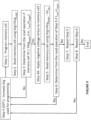
- the program compensation technique is implemented as part of the controller configuration for the memory array, which can be better understood from the architecture of an exemplary memory device as illustrated in Fig. 2 .
- the memory device includes an array 50 of the non-volatile memory cells 10, which can be segregated into two separate planes (Plane A 52a and Plane B 52b).
- the memory cells 10 can be of the type shown in Fig. 1 , formed on a single chip, arranged in a plurality of rows and columns in the semiconductor substrate 12.
- Adjacent to the array of non-volatile memory cells are address decoders (e.g. XDEC 54), a source line driver (e.g. SLDRV 56), a column decoder (e.g.
- YMUX 58 a high voltage row decoder (e.g. HVDEC 60) and a bit line controller (e.g. BLINHCTL 62), which are used to decode addresses and supply the various voltages to the various memory cell gates and regions during read, program, and erase operations for selected memory cells.
- Column decoder 58 includes a sense amplifier containing circuitry for measuring the currents on the bit lines during a read operation.
- Controller 66 (containing control circuitry) controls the various device elements to implement each operation (program, erase, read) on target memory cells.
- Charge pump CHRGPMP 64 provides the various voltages used to read, program and erase the memory cells under the control of the controller 66.
- Controller 66 is configured to operate the memory device to program, erase and read the memory cells 10. As part of these operations, the controller 66 can be provided with access to the incoming data which is data to be programmed to the memory cells, along with program, erase and read commands provided on the same or different lines. Data read from the memory array is provided as
- the program compensation technique involves the controller 66 implementing memory cell programming, and specifically providing additional programming for memory cells that exhibit an intolerable level of read current instability.
- This technique involves initially programming memory cell to a particular programming state and taking one or multiple measurements of a memory cell threshold voltage parameter (i.e., a minimum voltage applied to the memory cell to achieve a certain level of source/drain current, referred to as a target current I target ).
- the preferable threshold voltage parameter is Vtcg, which is the threshold voltage of the memory cell as viewed from the control gate 22.
- control gate threshold voltage Vtcg is the voltage on the control gate that results in the channel region being a conducting path, and therefore results in a read current through the channel of a predetermined amount (I target ) to consider the memory cell turned on (e.g., 1 ⁇ A) when the read potentials of a read operation are applied to the select gate 24 and drain region 16.
- the control gate threshold voltage Vtcg will vary as a function of programming state of the memory cell, but it is desired that once the memory cell is programmed to a particular programming state, any variation of Vtcg over time be below a predetermined amount.
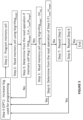
- Fig. 3 An embodiment of the programming technique is illustrated in Fig. 3 , which is implemented to program a memory cell to a specific programming state so that it has a target threshold voltage Vtcg target .
- the technique begins in Step 1 with programming performed on a memory cell (e.g., a memory cell 10 having the configuration shown in Fig. 1 ). As described above, this programming operation preferably involves applying programming voltages to the memory cell 10 for a limited time (i.e., in one or more pulses), which results in injecting electrons onto the floating gate 20.
- Step 2 a read operation is performed which involves applying read operation voltages to the memory cell 10 and measuring the current flowing through the channel region 18 of the memory cell 10.
- Step 3 it is determined from the read operation of Step 2 whether or not the threshold voltage Vtcg of the memory cell has reached or exceeded the target threshold voltage Vtcg target (i.e., whether the channel current I read is less than or equal to the target current I target , where I read equal to the target current I target is indicative of the threshold voltage Vtcg of the memory cell reaching the target threshold voltage Vtcg target ) If the determination is no (that the threshold voltage Vtcg is not greater than or equal to, i.e.
- Step 4 the voltage on the control gate Vcg used for programming is optionally increased, and then Step 1 is repeated. Steps 1-4 are repeated in order until it is determined in Step 3 that the threshold voltage Vtcg of the memory cell has reached or exceeded the target threshold voltage Vtcg target (i.e., that the channel current I read is less than or equal to the target current I target ). At that point, the memory cell is considered initially programmed to its desired programming state (i.e. to its target threshold voltage Vtcg target ). It is at this point where conventional programming usually ended.
- the programming state achieved by Steps 1-4 is only an initial programming state that may call for additional programming. Specifically, if the programmed memory cell exhibits RTN, then electron(s) captured in interface trap(s) contribute to the measured threshold voltage Vtcg of the memory cell as part of programming. If/when the electron(s) are emitted from the interface trap(s) after programming has ended, then the threshold voltage Vtcg could drop by more than ⁇ Vtcg max below the target threshold voltage Vtcg target , where ⁇ Vtcg max is the maximum tolerable read error in terms of Vtcg variation. A threshold voltage drop by more than ⁇ Vtcg max is considered to be an intolerable error during read operation.
- Step 5 the memory cell is read again, but this time using a control gate voltage Vcg that is less than the target threshold voltage Vtcg target used in Step 2.
- the control gate voltage Vcg used for this read operation is Vtcg target - ⁇ V tcg , where ⁇ V tcg is a relatively small amount and can be defined by the maximum tolerable read error.
- ⁇ V tcg can be equal to ⁇ Vtcg max which, in turn, depends on specific product and its application, and can be, as an example, 20 mV.
- Step 6 it is determined from the read operation of Step 5 whether or not the read current I read is greater than the target read current I target . If the memory cell does not exhibit intolerable RTN, then the small decrease in control gate voltage Vcg during the read operation should lower the read current I read further below I target , and the determination of Step 6 should be no. In that case, the memory cell can be considered properly programmed. However, if the memory cell does exhibit intolerable RTN, and if before or during this read operation there is interface trap electron emission, then the threshold voltage Vtcg of the memory cell will drop, resulting in a rise in read current I read . If that rise in current exceeds I target , then the memory cell is subjected to another round of programming starting at Step 4, and re-read again to confirm it is sufficiently programmed.
- the advantage of the above described technique is that if the memory cell exhibits intolerable RTN, then it will end up getting more deeply programmed (i.e. higher Vtcg) than would otherwise be the case. This means that even if electron emission occurs, it is less likely that the memory cell threshold voltage Vtcg will drop below the target threshold voltage Vtcg target exceeding the tolerance level of ⁇ Vtcg max . This is because the memory cell is more deeply programmed above Vtcg target and future read operations will more accurately reflect the desired programming state of the memory cell within the tolerance level of ⁇ Vtcg variations.
- the negative voltage will stimulate detrapping of electron, setting the threshold voltage Vtcg to a lower Vt state, and increasing the chances that the determination of Step 6 will be positive (and therefore the memory cell will be subjected to additional programming). Since RTN has an erratic behavior, a defective memory cell may stay in one Vtcg state during all read operations, whereby it will not be properly identified for additional programming. Therefore, application of a negative voltage (e.g., -1 V to -7 V) before the read operation of Step 5 will stimulate a memory cell with RTN to exhibit a lower Vt state and, thereby, be identified in Step 6 for additional programming, enhancing programming efficiency and accuracy.
- a negative voltage e.g., -1 V to -7 V
- Fig. 5 illustrates a second alternate embodiment, which is the same method as that described above and depicted in Fig. 4 for the first alternate embodiment, except the negative voltage is not only applied immediately before the initial read operation of Step 5, but it is also applied again before each repeated read operation of Step 5 (see Step 7, which repeats both Step 3A and Step 5, instead of just repeating just Step 5 as indicated in Fig. 4 ).
- threshold voltage Vt used in the above described techniques is Vtcg, which is the threshold voltage of the memory cell as viewed from the control gate 22.
- Vtcg the threshold voltage of the memory cell as viewed from the control gate 22.
- the above described techniques could be implemented with respect to threshold voltage Vt as viewed from any one or more gates in the memory cell that is not floating.
- the present invention could be implemented in an array of memory cells with fewer gates than those in Fig. 1 (e.g., no erase gate and/or control gate combined with select gate).
Landscapes
- Engineering & Computer Science (AREA)
- Computer Hardware Design (AREA)
- Read Only Memory (AREA)
- Non-Volatile Memory (AREA)
Claims (15)
- Speichervorrichtung, umfassend:eine Vielzahl nichtflüchtiger Speicherzellen (10), jeweils umfassend ein erstes Gate (22); undeine Steuereinrichtung (66), die konfiguriert ist, um eine nichtflüchtige Speicherzelle der Vielzahl von nichtflüchtigen Speicherzellen zu programmieren durch:Programmieren der einen nichtflüchtigen Speicherzelle in einen anfänglichen Programmzustand, der einem Erreichen oder einem Überschreiten einer Zielschwellenspannung für das erste Gate der einen nichtflüchtigen Speicherzelle entspricht, wobei die Zielschwellenspannung einem Ziellesestrom entspricht,Lesen der einen nichtflüchtigen Speicherzelle in einem ersten Lesevorgang unter Verwendung einer Lesespannung, die an das erste Gate der einen nichtflüchtigen Speicherzelle angelegt wird, die kleiner als die Zielschwellenspannung ist, um einen ersten Lesestrom zu erzeugen, undUnterziehen der einen nichtflüchtigen Speicherzelle einem zusätzlichen Programmieren als Reaktion auf ein Bestimmen, dass der erste Lesestrom größer als der Ziellesestrom ist;Lesen der einen nichtflüchtigen Speicherzelle in einem zweiten Lesevorgang als Reaktion auf das Bestimmen, dass der erste Lesestrom nicht größer als der Ziellesestrom in dem ersten Lesevorgang ist, unter Verwendung einer Lesespannung, die an das erste Gate der einen nichtflüchtigen Speicherzelle angelegt wird, die kleiner als die Zielschwellenspannung ist, um einen zweiten Lesestrom zu erzeugen, undUnterziehen der einen nichtflüchtigen Speicherzelle dem zusätzlichen Programmieren als Reaktion auf das Bestimmen, dass der zweite Lesestrom größer als der Ziellesestrom ist.
- Vorrichtung nach Anspruch 1, wobei die Steuereinrichtung konfiguriert ist, um das Programmieren der einen nichtflüchtigen Speicherzelle in den anfänglichen Programmzustand durch folgende Schritte durchzuführen:Anlegen von mindestens einem ersten Impuls von Programmierspannungen an die eine nichtflüchtige Speicherzelle;Lesen der einen nichtflüchtigen Speicherzelle unter Verwendung einer Lesespannung, die an das erste Gate der einen nichtflüchtigen Speicherzelle angelegt wird, die gleich der Zielschwellenspannung ist, um einen zweiten Lesestrom zu erzeugen; undAnlegen von mindestens einem zweiten Impuls von Programmierspannungen an die eine nichtflüchtige Speicherzelle als Reaktion auf das Bestimmen, dass der zweite Lesestrom größer als der Ziellesestrom ist.
- Vorrichtung nach Anspruch 2, wobei eine Spannung, die als Teil des zweiten Impulses von Programmierspannungen an das erste Gate angelegt wird, größer als eine Spannung ist, die als Teil des ersten Impulses von Programmierspannungen an das erste Gate angelegt wird.
- Vorrichtung nach Anspruch 1, wobei jede der Vielzahl von nichtflüchtigen Speicherzellen ein zweites Gate (24, 26) umfasst, und wobei die Steuereinrichtung ferner konfiguriert ist, um nach dem Programmieren der einen nichtflüchtigen Speicherzelle in den anfänglichen Programmzustand und vor dem ersten Lesevorgang eine negative Spannung an das zweite Gate der einen nichtflüchtigen Speicherzelle anzulegen.
- Vorrichtung nach Anspruch 1, wobei die Steuereinrichtung ferner konfiguriert ist, um nach dem Programmieren der einen nichtflüchtigen Speicherzelle in den anfänglichen Programmzustand und vor dem ersten Lesevorgang eine negative Spannung an das erste Gate der einen nichtflüchtigen Speicherzelle anzulegen.
- Vorrichtung nach Anspruch 1, wobei jede der Vielzahl von nichtflüchtigen Speicherzellen ein zweites Gate (24, 26) umfasst, und wobei die Steuereinrichtung ferner konfiguriert ist zum:Anlegen einer negativen Spannung an das zweite Gate der einen nichtflüchtigen Speicherzelle nach dem Programmieren der einen nichtflüchtigen Speicherzelle in den anfänglichen Programmzustand und vor dem ersten Lesevorgang; undAnlegen einer negativen Spannung an das zweite Gate der einen nichtflüchtigen Speicherzelle nach dem Bestimmen, dass der erste Lesestrom nicht größer als der Ziellesestrom in dem ersten Lesevorgang und vor dem zweiten Lesevorgang ist.
- Vorrichtung nach Anspruch 1, wobei die Steuereinrichtung ferner konfiguriert ist zum:Anlegen einer negativen Spannung an das erste Gate der einen nichtflüchtigen Speicherzelle nach dem Programmieren der einen nichtflüchtigen Speicherzelle in den anfänglichen Programmzustand und vor dem ersten Lesevorgang; undAnlegen einer negativen Spannung an das erste Gate der einen nichtflüchtigen Speicherzelle nach dem Bestimmen, dass der erste Lesestrom nicht größer als der Ziellesestrom in dem ersten Lesevorgang und vor dem zweiten Lesevorgang ist.
- Verfahren zum Programmieren einer nichtflüchtigen Speicherzelle aus einer Vielzahl von nichtflüchtigen Speicherzellen (10), wobei jede der Vielzahl von nichtflüchtigen Speicherzellen ein erstes Gate (22) einschließt, das Verfahren umfassend:Programmieren der einen nichtflüchtigen Speicherzelle in einen anfänglichen Programmzustand, der dem Erreichen oder dem Überschreiten einer Zielschwellenspannung für das erste Gate der einen nichtflüchtigen Speicherzelle entspricht, wobei die Zielschwellenspannung einem Ziellesestrom entspricht,Lesen der einen nichtflüchtigen Speicherzelle in einem ersten Lesevorgang unter Verwendung einer Lesespannung, die an das erste Gate der einen nichtflüchtigen Speicherzelle angelegt wird, die kleiner als die Zielschwellenspannung ist, um einen ersten Lesestrom zu erzeugen, undUnterziehen der einen nichtflüchtigen Speicherzelle dem zusätzlichen Programmieren als Reaktion auf das Bestimmen, dass der erste Lesestrom größer als der Ziellesestrom ist;Lesen der einen nichtflüchtigen Speicherzelle in einem zweiten Lesevorgang als Reaktion auf das Bestimmen, dass der erste Lesestrom nicht größer als der Ziellesestrom in dem ersten Lesevorgang ist, unter Verwendung einer Lesespannung, die an das erste Gate der einen nichtflüchtigen Speicherzelle angelegt wird, die kleiner als die Zielschwellenspannung ist, um einen zweiten Lesestrom zu erzeugen, undUnterziehen der einen nichtflüchtigen Speicherzelle dem zusätzlichen Programmieren als Reaktion auf das Bestimmen, dass der zweite Lesestrom größer als der Ziellesestrom ist.
- Vorrichtung nach Anspruch 1 oder Verfahren nach Anspruch 8, wobei jede der Vielzahl von nichtflüchtigen Speicherzellen ferner umfasst:voneinander beabstandete Source- und Drain-Regionen (14, 16), die in einem Halbleitersubstrat (12) ausgebildet sind, wobei sich eine Kanalregion (18) des Substrats dazwischen erstreckt;ein Floating-Gate (20), das über einem ersten Abschnitt der Kanalregion vertikal angeordnet und von diesem isoliert ist; undein Auswahl-Gate (24), das über einem zweiten Abschnitt der Kanalregion vertikal angeordnet und von diesem isoliert ist;wobei für jede der Vielzahl von nichtflüchtigen Speicherzellen das erste Gate vertikal über dem Floating Gate angeordnet und von diesem isoliert ist.
- Vorrichtung nach Anspruch 1 oder Verfahren nach Anspruch 8, wobei jede der Vielzahl von nichtflüchtigen Speicherzellen ferner umfasst:
ein Lösch-Gate (26), das über der Source-Region angeordnet und von dieser isoliert ist. - Verfahren nach Anspruch 8, wobei das Programmieren der einen nichtflüchtigen Speicherzelle in den anfänglichen Programmzustand umfasst:Anlegen von mindestens einem ersten Impuls von Programmierspannungen an die eine nichtflüchtige Speicherzelle;Lesen der einen nichtflüchtigen Speicherzelle unter Verwendung einer Lesespannung, die an das erste Gate der einen nichtflüchtigen Speicherzelle angelegt wird, die gleich der Zielschwellenspannung ist, um einen zweiten Lesestrom zu erzeugen; undAnlegen von mindestens einem zweiten Impuls von Programmierspannungen an die eine nichtflüchtige Speicherzelle als Reaktion auf das Bestimmen, dass der zweite Lesestrom größer als der Ziellesestrom ist.
- Verfahren nach Anspruch 11, wobei eine Spannung, die als Teil des zweiten Impulses von Programmierspannungen an das erste Gate angelegt wird, größer als eine Spannung ist, die als Teil des ersten Impulses von Programmierspannungen an das erste Gate angelegt wird.
- Verfahren nach Anspruch 8, wobei jede der Vielzahl von nichtflüchtigen Speicherzellen ein zweites Gate umfasst, das Verfahren ferner umfassend:
Anlegen einer negativen Spannung an das zweite Gate der einen nichtflüchtigen Speicherzelle nach dem Programmieren der einen nichtflüchtigen Speicherzelle in den anfänglichen Programmzustand und vor dem ersten Lesevorgang. - Verfahren nach Anspruch 8, ferner umfassend:
Anlegen einer negativen Spannung an das erste Gate der einen nichtflüchtigen Speicherzelle nach dem Programmieren der einen nichtflüchtigen Speicherzelle in den anfänglichen Programmzustand und vor dem ersten Lesevorgang. - Verfahren nach Anspruch 8, wobei jede der Vielzahl von nichtflüchtigen Speicherzellen ein zweites Gate umfasst, das Verfahren ferner umfassend:Anlegen einer negativen Spannung an das zweite Gate der einen nichtflüchtigen Speicherzelle nach dem Programmieren der einen nichtflüchtigen Speicherzelle in den anfänglichen Programmzustand und vor dem ersten Lesevorgang; undAnlegen einer negativen Spannung an das zweite Gate der einen nichtflüchtigen Speicherzelle nach dem Bestimmen, dass der erste Lesestrom nicht größer als der Ziellesestrom in dem ersten Lesevorgang und vor dem zweiten Lesevorgang ist, und/oderAnlegen einer negativen Spannung an das erste Gate der einen nichtflüchtigen Speicherzelle nach dem Programmieren der einen nichtflüchtigen Speicherzelle in den anfänglichen Programmzustand und vor dem ersten Lesevorgang; undAnlegen einer negativen Spannung an das erste Gate der einen nichtflüchtigen Speicherzelle nach dem Bestimmen, dass der erste Lesestrom nicht größer als der Ziellesestrom in dem ersten Lesevorgang und vor dem zweiten Lesevorgang ist.
Applications Claiming Priority (2)
| Application Number | Priority Date | Filing Date | Title |
|---|---|---|---|
| US16/915,289 US11309042B2 (en) | 2020-06-29 | 2020-06-29 | Method of improving read current stability in analog non-volatile memory by program adjustment for memory cells exhibiting random telegraph noise |
| PCT/US2021/017007 WO2022005534A1 (en) | 2020-06-29 | 2021-02-08 | Method of improving read current stability in analog non-volatile memory by program adjustment for memory cells exhibiting random telegraph noise |
Publications (2)
| Publication Number | Publication Date |
|---|---|
| EP4172989A1 EP4172989A1 (de) | 2023-05-03 |
| EP4172989B1 true EP4172989B1 (de) | 2024-12-04 |
Family
ID=74845105
Family Applications (1)
| Application Number | Title | Priority Date | Filing Date |
|---|---|---|---|
| EP21709282.4A Active EP4172989B1 (de) | 2020-06-29 | 2021-02-08 | Verfahren zur verbesserung der lesestromstabilität in einem analogen nichtflüchtigen speicher durch programmanpassung für speicherzellen mit zufälligem telegrafischem rauschen |
Country Status (7)
| Country | Link |
|---|---|
| US (1) | US11309042B2 (de) |
| EP (1) | EP4172989B1 (de) |
| JP (1) | JP7474876B2 (de) |
| KR (1) | KR20230002957A (de) |
| CN (1) | CN115720672A (de) |
| TW (1) | TWI773334B (de) |
| WO (1) | WO2022005534A1 (de) |
Families Citing this family (7)
| Publication number | Priority date | Publication date | Assignee | Title |
|---|---|---|---|---|
| US12158814B2 (en) * | 2014-08-07 | 2024-12-03 | Pure Storage, Inc. | Granular voltage tuning |
| US11728000B1 (en) * | 2017-12-13 | 2023-08-15 | Board Of Trustees Of The University Of Alabama, For And On Behalf Of The University Of Alabama In Huntsville | Systems and methods for detecting counterfeit or defective memory |
| US12159053B1 (en) | 2021-05-24 | 2024-12-03 | Board of Trustees for the University of Alabama, for and on behalf of the University of Alabama in Huntsville | Systems and methods for identifying counterfeit memory |
| US11769558B2 (en) * | 2021-06-08 | 2023-09-26 | Silicon Storage Technology, Inc. | Method of reducing random telegraph noise in non-volatile memory by grouping and screening memory cells |
| CN114912154B (zh) * | 2022-06-06 | 2024-03-15 | 山东大学 | 一种基于非易失存储器的加密存算一体的实现方法 |
| KR20240017546A (ko) * | 2022-08-01 | 2024-02-08 | 에스케이하이닉스 주식회사 | 메모리 장치 및 이의 동작 방법 |
| US12511073B2 (en) | 2024-01-12 | 2025-12-30 | Silicon Storage Technology, Inc. | Coarse and fine programming of non-volatile memory cells |
Family Cites Families (29)
| Publication number | Priority date | Publication date | Assignee | Title |
|---|---|---|---|---|
| US5029130A (en) | 1990-01-22 | 1991-07-02 | Silicon Storage Technology, Inc. | Single transistor non-valatile electrically alterable semiconductor memory device |
| KR100276653B1 (ko) * | 1998-08-27 | 2001-01-15 | 윤종용 | 스프릿 게이트형 불휘발성 메모리 셀의 구동방법 및 이 셀들을구비한 반도체 메모리 장치의 구동방법 |
| US6727545B2 (en) | 2000-09-20 | 2004-04-27 | Silicon Storage Technology, Inc. | Semiconductor memory array of floating gate memory cells with low resistance source regions and high source coupling |
| KR100456596B1 (ko) * | 2002-05-08 | 2004-11-09 | 삼성전자주식회사 | 부유트랩형 비휘발성 기억소자의 소거 방법 |
| US6747310B2 (en) | 2002-10-07 | 2004-06-08 | Actrans System Inc. | Flash memory cells with separated self-aligned select and erase gates, and process of fabrication |
| US7177199B2 (en) | 2003-10-20 | 2007-02-13 | Sandisk Corporation | Behavior based programming of non-volatile memory |
| US7315056B2 (en) | 2004-06-07 | 2008-01-01 | Silicon Storage Technology, Inc. | Semiconductor memory array of floating gate memory cells with program/erase and select gates |
| KR100769258B1 (ko) * | 2006-10-23 | 2007-10-22 | 삼성전자주식회사 | 문턱 전압 분포를 줄일 수 있는 불 휘발성 메모리 장치 |
| KR100799018B1 (ko) | 2006-12-27 | 2008-01-28 | 주식회사 하이닉스반도체 | 불휘발성 메모리 소자 및 자기 보상 방법 |
| US20090039410A1 (en) | 2007-08-06 | 2009-02-12 | Xian Liu | Split Gate Non-Volatile Flash Memory Cell Having A Floating Gate, Control Gate, Select Gate And An Erase Gate With An Overhang Over The Floating Gate, Array And Method Of Manufacturing |
| KR101490426B1 (ko) * | 2008-11-14 | 2015-02-06 | 삼성전자주식회사 | 불휘발성 메모리 장치 및 그것의 읽기 방법 |
| US8223555B2 (en) | 2009-05-07 | 2012-07-17 | Micron Technology, Inc. | Multiple level program verify in a memory device |
| JP2011070712A (ja) * | 2009-09-24 | 2011-04-07 | Toshiba Corp | Nand型フラッシュメモリ |
| KR101666941B1 (ko) * | 2010-07-06 | 2016-10-17 | 삼성전자주식회사 | 비휘발성 메모리 장치와 이를 포함하는 반도체 시스템 |
| US8842469B2 (en) | 2010-11-09 | 2014-09-23 | Freescale Semiconductor, Inc. | Method for programming a multi-state non-volatile memory (NVM) |
| US8711636B2 (en) | 2011-05-13 | 2014-04-29 | Silicon Storage Technology, Inc. | Method of operating a split gate flash memory cell with coupling gate |
| KR20130016619A (ko) * | 2011-08-08 | 2013-02-18 | 삼성전자주식회사 | 불휘발성 메모리 장치의 프로그램 방법 |
| GB201301622D0 (en) * | 2013-01-30 | 2013-03-13 | Ibm | Method and apparatus for read measurement of a plurarity of resistive memory cells |
| US8675405B1 (en) * | 2013-03-12 | 2014-03-18 | Cypress Semiconductor Corp. | Method to reduce program disturbs in non-volatile memory cells |
| JP5964522B2 (ja) * | 2013-03-14 | 2016-08-03 | シリコン ストーリッジ テクノロージー インコーポレイテッドSilicon Storage Technology, Inc. | 不揮発性メモリのプログラムアルゴリズムのデバイス及び方法 |
| US8908441B1 (en) | 2013-10-15 | 2014-12-09 | Sandisk Technologies Inc. | Double verify method in multi-pass programming to suppress read noise |
| KR20150109120A (ko) * | 2014-03-19 | 2015-10-01 | 에스케이하이닉스 주식회사 | 반도체 메모리 장치 및 이의 동작 방법 |
| US9343141B2 (en) | 2014-07-15 | 2016-05-17 | Sandisk Technologies Inc. | Reprogramming memory with single program pulse per data state |
| US9830219B2 (en) * | 2014-09-15 | 2017-11-28 | Western Digital Technologies, Inc. | Encoding scheme for 3D vertical flash memory |
| US9721672B1 (en) * | 2016-04-15 | 2017-08-01 | Sandisk Technologies Llc | Multi-die programming with die-jumping induced periodic delays |
| KR102182583B1 (ko) * | 2016-05-17 | 2020-11-24 | 실리콘 스토리지 테크놀로지 인크 | 비휘발성 메모리 어레이를 사용하는 딥러닝 신경망 분류기 |
| US10460797B2 (en) * | 2017-09-08 | 2019-10-29 | Macronix International Co., Ltd. | Method for programming non-volatile memory and memory system |
| US10838652B2 (en) | 2018-08-24 | 2020-11-17 | Silicon Storage Technology, Inc. | Programming of memory cell having gate capacitively coupled to floating gate |
| TW202025165A (zh) * | 2018-12-22 | 2020-07-01 | 大陸商深圳大心電子科技有限公司 | 資料讀取方法、儲存控制器與儲存裝置 |
-
2020
- 2020-06-29 US US16/915,289 patent/US11309042B2/en active Active
-
2021
- 2021-02-08 CN CN202180046206.6A patent/CN115720672A/zh active Pending
- 2021-02-08 EP EP21709282.4A patent/EP4172989B1/de active Active
- 2021-02-08 JP JP2022580154A patent/JP7474876B2/ja active Active
- 2021-02-08 KR KR1020227040788A patent/KR20230002957A/ko active Pending
- 2021-02-08 WO PCT/US2021/017007 patent/WO2022005534A1/en not_active Ceased
- 2021-05-21 TW TW110118467A patent/TWI773334B/zh active
Also Published As
| Publication number | Publication date |
|---|---|
| US11309042B2 (en) | 2022-04-19 |
| JP7474876B2 (ja) | 2024-04-25 |
| TW202201408A (zh) | 2022-01-01 |
| JP2023532022A (ja) | 2023-07-26 |
| EP4172989A1 (de) | 2023-05-03 |
| TWI773334B (zh) | 2022-08-01 |
| KR20230002957A (ko) | 2023-01-05 |
| WO2022005534A1 (en) | 2022-01-06 |
| CN115720672A (zh) | 2023-02-28 |
| US20210407602A1 (en) | 2021-12-30 |
Similar Documents
| Publication | Publication Date | Title |
|---|---|---|
| EP4172989B1 (de) | Verfahren zur verbesserung der lesestromstabilität in einem analogen nichtflüchtigen speicher durch programmanpassung für speicherzellen mit zufälligem telegrafischem rauschen | |
| EP4026129B1 (de) | Verfahren zur verbesserung der lesestromstabilität in einem analogen nichtflüchtigen speicher durch screening von speicherzellen | |
| EP4352728B1 (de) | Verfahren zur reduzierung von zufälligem telegrafischem rauschen in einem nichtflüchtigen speicher durch gruppierung und screening von speicherzellen | |
| EP4348651B1 (de) | Verfahren zur verbesserung der lesestromstabilität in einem analogen nichtflüchtigen speicher durch nachprogrammierungsabstimmung von speicherzellen mit zufälligem telegrafischem rauschen | |
| US12080355B2 (en) | Method of improving read current stability in analog non-volatile memory by post-program tuning for memory cells exhibiting random telegraph noise | |
| WO2022260692A1 (en) | Method of reducing random telegraph noise in non-volatile memory by grouping and screening memory cells |
Legal Events
| Date | Code | Title | Description |
|---|---|---|---|
| STAA | Information on the status of an ep patent application or granted ep patent |
Free format text: STATUS: UNKNOWN |
|
| STAA | Information on the status of an ep patent application or granted ep patent |
Free format text: STATUS: THE INTERNATIONAL PUBLICATION HAS BEEN MADE |
|
| PUAI | Public reference made under article 153(3) epc to a published international application that has entered the european phase |
Free format text: ORIGINAL CODE: 0009012 |
|
| STAA | Information on the status of an ep patent application or granted ep patent |
Free format text: STATUS: REQUEST FOR EXAMINATION WAS MADE |
|
| 17P | Request for examination filed |
Effective date: 20230127 |
|
| AK | Designated contracting states |
Kind code of ref document: A1 Designated state(s): AL AT BE BG CH CY CZ DE DK EE ES FI FR GB GR HR HU IE IS IT LI LT LU LV MC MK MT NL NO PL PT RO RS SE SI SK SM TR |
|
| DAV | Request for validation of the european patent (deleted) | ||
| DAX | Request for extension of the european patent (deleted) | ||
| STAA | Information on the status of an ep patent application or granted ep patent |
Free format text: STATUS: EXAMINATION IS IN PROGRESS |
|
| 17Q | First examination report despatched |
Effective date: 20240214 |
|
| GRAP | Despatch of communication of intention to grant a patent |
Free format text: ORIGINAL CODE: EPIDOSNIGR1 |
|
| STAA | Information on the status of an ep patent application or granted ep patent |
Free format text: STATUS: GRANT OF PATENT IS INTENDED |
|
| INTG | Intention to grant announced |
Effective date: 20240820 |
|
| GRAS | Grant fee paid |
Free format text: ORIGINAL CODE: EPIDOSNIGR3 |
|
| GRAA | (expected) grant |
Free format text: ORIGINAL CODE: 0009210 |
|
| STAA | Information on the status of an ep patent application or granted ep patent |
Free format text: STATUS: THE PATENT HAS BEEN GRANTED |
|
| AK | Designated contracting states |
Kind code of ref document: B1 Designated state(s): AL AT BE BG CH CY CZ DE DK EE ES FI FR GB GR HR HU IE IS IT LI LT LU LV MC MK MT NL NO PL PT RO RS SE SI SK SM TR |
|
| P01 | Opt-out of the competence of the unified patent court (upc) registered |
Free format text: CASE NUMBER: APP_59036/2024 Effective date: 20241029 |
|
| REG | Reference to a national code |
Ref country code: CH Ref legal event code: EP |
|
| REG | Reference to a national code |
Ref country code: DE Ref legal event code: R096 Ref document number: 602021022833 Country of ref document: DE |
|
| REG | Reference to a national code |
Ref country code: IE Ref legal event code: FG4D |
|
| PGFP | Annual fee paid to national office [announced via postgrant information from national office to epo] |
Ref country code: NL Payment date: 20250121 Year of fee payment: 5 |
|
| REG | Reference to a national code |
Ref country code: NL Ref legal event code: FP |
|
| REG | Reference to a national code |
Ref country code: LT Ref legal event code: MG9D |
|
| PG25 | Lapsed in a contracting state [announced via postgrant information from national office to epo] |
Ref country code: HR Free format text: LAPSE BECAUSE OF FAILURE TO SUBMIT A TRANSLATION OF THE DESCRIPTION OR TO PAY THE FEE WITHIN THE PRESCRIBED TIME-LIMIT Effective date: 20241204 |
|
| PGFP | Annual fee paid to national office [announced via postgrant information from national office to epo] |
Ref country code: DE Payment date: 20250122 Year of fee payment: 5 |
|
| PG25 | Lapsed in a contracting state [announced via postgrant information from national office to epo] |
Ref country code: FI Free format text: LAPSE BECAUSE OF FAILURE TO SUBMIT A TRANSLATION OF THE DESCRIPTION OR TO PAY THE FEE WITHIN THE PRESCRIBED TIME-LIMIT Effective date: 20241204 |
|
| PG25 | Lapsed in a contracting state [announced via postgrant information from national office to epo] |
Ref country code: BG Free format text: LAPSE BECAUSE OF FAILURE TO SUBMIT A TRANSLATION OF THE DESCRIPTION OR TO PAY THE FEE WITHIN THE PRESCRIBED TIME-LIMIT Effective date: 20241204 |
|
| PG25 | Lapsed in a contracting state [announced via postgrant information from national office to epo] |
Ref country code: ES Free format text: LAPSE BECAUSE OF FAILURE TO SUBMIT A TRANSLATION OF THE DESCRIPTION OR TO PAY THE FEE WITHIN THE PRESCRIBED TIME-LIMIT Effective date: 20241204 |
|
| PG25 | Lapsed in a contracting state [announced via postgrant information from national office to epo] |
Ref country code: NO Free format text: LAPSE BECAUSE OF FAILURE TO SUBMIT A TRANSLATION OF THE DESCRIPTION OR TO PAY THE FEE WITHIN THE PRESCRIBED TIME-LIMIT Effective date: 20250304 |
|
| PG25 | Lapsed in a contracting state [announced via postgrant information from national office to epo] |
Ref country code: LV Free format text: LAPSE BECAUSE OF FAILURE TO SUBMIT A TRANSLATION OF THE DESCRIPTION OR TO PAY THE FEE WITHIN THE PRESCRIBED TIME-LIMIT Effective date: 20241204 Ref country code: GR Free format text: LAPSE BECAUSE OF FAILURE TO SUBMIT A TRANSLATION OF THE DESCRIPTION OR TO PAY THE FEE WITHIN THE PRESCRIBED TIME-LIMIT Effective date: 20250305 |
|
| PGFP | Annual fee paid to national office [announced via postgrant information from national office to epo] |
Ref country code: FR Payment date: 20250121 Year of fee payment: 5 |
|
| PG25 | Lapsed in a contracting state [announced via postgrant information from national office to epo] |
Ref country code: RS Free format text: LAPSE BECAUSE OF FAILURE TO SUBMIT A TRANSLATION OF THE DESCRIPTION OR TO PAY THE FEE WITHIN THE PRESCRIBED TIME-LIMIT Effective date: 20250304 |
|
| REG | Reference to a national code |
Ref country code: AT Ref legal event code: MK05 Ref document number: 1749051 Country of ref document: AT Kind code of ref document: T Effective date: 20241204 |
|
| PG25 | Lapsed in a contracting state [announced via postgrant information from national office to epo] |
Ref country code: SM Free format text: LAPSE BECAUSE OF FAILURE TO SUBMIT A TRANSLATION OF THE DESCRIPTION OR TO PAY THE FEE WITHIN THE PRESCRIBED TIME-LIMIT Effective date: 20241204 |
|
| PG25 | Lapsed in a contracting state [announced via postgrant information from national office to epo] |
Ref country code: PL Free format text: LAPSE BECAUSE OF FAILURE TO SUBMIT A TRANSLATION OF THE DESCRIPTION OR TO PAY THE FEE WITHIN THE PRESCRIBED TIME-LIMIT Effective date: 20241204 |
|
| PG25 | Lapsed in a contracting state [announced via postgrant information from national office to epo] |
Ref country code: IS Free format text: LAPSE BECAUSE OF FAILURE TO SUBMIT A TRANSLATION OF THE DESCRIPTION OR TO PAY THE FEE WITHIN THE PRESCRIBED TIME-LIMIT Effective date: 20250404 |
|
| PG25 | Lapsed in a contracting state [announced via postgrant information from national office to epo] |
Ref country code: PT Free format text: LAPSE BECAUSE OF FAILURE TO SUBMIT A TRANSLATION OF THE DESCRIPTION OR TO PAY THE FEE WITHIN THE PRESCRIBED TIME-LIMIT Effective date: 20250404 |
|
| PG25 | Lapsed in a contracting state [announced via postgrant information from national office to epo] |
Ref country code: EE Free format text: LAPSE BECAUSE OF FAILURE TO SUBMIT A TRANSLATION OF THE DESCRIPTION OR TO PAY THE FEE WITHIN THE PRESCRIBED TIME-LIMIT Effective date: 20241204 |
|
| PG25 | Lapsed in a contracting state [announced via postgrant information from national office to epo] |
Ref country code: RO Free format text: LAPSE BECAUSE OF FAILURE TO SUBMIT A TRANSLATION OF THE DESCRIPTION OR TO PAY THE FEE WITHIN THE PRESCRIBED TIME-LIMIT Effective date: 20241204 Ref country code: AT Free format text: LAPSE BECAUSE OF FAILURE TO SUBMIT A TRANSLATION OF THE DESCRIPTION OR TO PAY THE FEE WITHIN THE PRESCRIBED TIME-LIMIT Effective date: 20241204 |
|
| PG25 | Lapsed in a contracting state [announced via postgrant information from national office to epo] |
Ref country code: SK Free format text: LAPSE BECAUSE OF FAILURE TO SUBMIT A TRANSLATION OF THE DESCRIPTION OR TO PAY THE FEE WITHIN THE PRESCRIBED TIME-LIMIT Effective date: 20241204 |
|
| PG25 | Lapsed in a contracting state [announced via postgrant information from national office to epo] |
Ref country code: CZ Free format text: LAPSE BECAUSE OF FAILURE TO SUBMIT A TRANSLATION OF THE DESCRIPTION OR TO PAY THE FEE WITHIN THE PRESCRIBED TIME-LIMIT Effective date: 20241204 |
|
| PG25 | Lapsed in a contracting state [announced via postgrant information from national office to epo] |
Ref country code: IT Free format text: LAPSE BECAUSE OF FAILURE TO SUBMIT A TRANSLATION OF THE DESCRIPTION OR TO PAY THE FEE WITHIN THE PRESCRIBED TIME-LIMIT Effective date: 20241204 |
|
| REG | Reference to a national code |
Ref country code: DE Ref legal event code: R097 Ref document number: 602021022833 Country of ref document: DE |
|
| PG25 | Lapsed in a contracting state [announced via postgrant information from national office to epo] |
Ref country code: SE Free format text: LAPSE BECAUSE OF FAILURE TO SUBMIT A TRANSLATION OF THE DESCRIPTION OR TO PAY THE FEE WITHIN THE PRESCRIBED TIME-LIMIT Effective date: 20241204 |
|
| PG25 | Lapsed in a contracting state [announced via postgrant information from national office to epo] |
Ref country code: MC Free format text: LAPSE BECAUSE OF FAILURE TO SUBMIT A TRANSLATION OF THE DESCRIPTION OR TO PAY THE FEE WITHIN THE PRESCRIBED TIME-LIMIT Effective date: 20241204 |
|
| REG | Reference to a national code |
Ref country code: CH Ref legal event code: PL |
|
| PG25 | Lapsed in a contracting state [announced via postgrant information from national office to epo] |
Ref country code: DK Free format text: LAPSE BECAUSE OF FAILURE TO SUBMIT A TRANSLATION OF THE DESCRIPTION OR TO PAY THE FEE WITHIN THE PRESCRIBED TIME-LIMIT Effective date: 20241204 |
|
| PLBE | No opposition filed within time limit |
Free format text: ORIGINAL CODE: 0009261 |
|
| STAA | Information on the status of an ep patent application or granted ep patent |
Free format text: STATUS: NO OPPOSITION FILED WITHIN TIME LIMIT |
|
| PG25 | Lapsed in a contracting state [announced via postgrant information from national office to epo] |
Ref country code: LU Free format text: LAPSE BECAUSE OF NON-PAYMENT OF DUE FEES Effective date: 20250208 |
|
| PG25 | Lapsed in a contracting state [announced via postgrant information from national office to epo] |
Ref country code: CH Free format text: LAPSE BECAUSE OF NON-PAYMENT OF DUE FEES Effective date: 20250228 |
|
| 26N | No opposition filed |
Effective date: 20250905 |
|
| GBPC | Gb: european patent ceased through non-payment of renewal fee |
Effective date: 20250304 |
|
| REG | Reference to a national code |
Ref country code: BE Ref legal event code: MM Effective date: 20250228 |
|
| PG25 | Lapsed in a contracting state [announced via postgrant information from national office to epo] |
Ref country code: GB Free format text: LAPSE BECAUSE OF NON-PAYMENT OF DUE FEES Effective date: 20250304 |
|
| PG25 | Lapsed in a contracting state [announced via postgrant information from national office to epo] |
Ref country code: BE Free format text: LAPSE BECAUSE OF NON-PAYMENT OF DUE FEES Effective date: 20250228 |
|
| PG25 | Lapsed in a contracting state [announced via postgrant information from national office to epo] |
Ref country code: IE Free format text: LAPSE BECAUSE OF NON-PAYMENT OF DUE FEES Effective date: 20250208 |