EP4348651B1 - Verfahren zur verbesserung der lesestromstabilität in einem analogen nichtflüchtigen speicher durch nachprogrammierungsabstimmung von speicherzellen mit zufälligem telegrafischem rauschen - Google Patents
Verfahren zur verbesserung der lesestromstabilität in einem analogen nichtflüchtigen speicher durch nachprogrammierungsabstimmung von speicherzellen mit zufälligem telegrafischem rauschen Download PDFInfo
- Publication number
- EP4348651B1 EP4348651B1 EP21795151.6A EP21795151A EP4348651B1 EP 4348651 B1 EP4348651 B1 EP 4348651B1 EP 21795151 A EP21795151 A EP 21795151A EP 4348651 B1 EP4348651 B1 EP 4348651B1
- Authority
- EP
- European Patent Office
- Prior art keywords
- memory cell
- volatile memory
- gate
- selected non
- read
- Prior art date
- Legal status (The legal status is an assumption and is not a legal conclusion. Google has not performed a legal analysis and makes no representation as to the accuracy of the status listed.)
- Active
Links
Images


Classifications
-
- G—PHYSICS
- G11—INFORMATION STORAGE
- G11C—STATIC STORES
- G11C16/00—Erasable programmable read-only memories
- G11C16/02—Erasable programmable read-only memories electrically programmable
- G11C16/04—Erasable programmable read-only memories electrically programmable using variable threshold transistors, e.g. FAMOS
- G11C16/0408—Erasable programmable read-only memories electrically programmable using variable threshold transistors, e.g. FAMOS comprising cells containing floating gate transistors
- G11C16/0425—Erasable programmable read-only memories electrically programmable using variable threshold transistors, e.g. FAMOS comprising cells containing floating gate transistors comprising cells containing a merged floating gate and select transistor
-
- G—PHYSICS
- G11—INFORMATION STORAGE
- G11C—STATIC STORES
- G11C16/00—Erasable programmable read-only memories
- G11C16/02—Erasable programmable read-only memories electrically programmable
- G11C16/06—Auxiliary circuits, e.g. for writing into memory
- G11C16/10—Programming or data input circuits
-
- G—PHYSICS
- G11—INFORMATION STORAGE
- G11C—STATIC STORES
- G11C16/00—Erasable programmable read-only memories
- G11C16/02—Erasable programmable read-only memories electrically programmable
- G11C16/06—Auxiliary circuits, e.g. for writing into memory
- G11C16/34—Determination of programming status, e.g. threshold voltage, overprogramming or underprogramming, retention
- G11C16/3418—Disturbance prevention or evaluation; Refreshing of disturbed memory data
-
- G—PHYSICS
- G11—INFORMATION STORAGE
- G11C—STATIC STORES
- G11C16/00—Erasable programmable read-only memories
- G11C16/02—Erasable programmable read-only memories electrically programmable
- G11C16/06—Auxiliary circuits, e.g. for writing into memory
- G11C16/34—Determination of programming status, e.g. threshold voltage, overprogramming or underprogramming, retention
- G11C16/3436—Arrangements for verifying correct programming or erasure
- G11C16/3454—Arrangements for verifying correct programming or for detecting overprogrammed cells
- G11C16/3459—Circuits or methods to verify correct programming of nonvolatile memory cells
-
- G—PHYSICS
- G11—INFORMATION STORAGE
- G11C—STATIC STORES
- G11C11/00—Digital stores characterised by the use of particular electric or magnetic storage elements; Storage elements therefor
- G11C11/56—Digital stores characterised by the use of particular electric or magnetic storage elements; Storage elements therefor using storage elements with more than two stable states represented by steps, e.g. of voltage, current, phase, frequency
- G11C11/5621—Digital stores characterised by the use of particular electric or magnetic storage elements; Storage elements therefor using storage elements with more than two stable states represented by steps, e.g. of voltage, current, phase, frequency using charge storage in a floating gate
- G11C11/5628—Programming or writing circuits; Data input circuits
-
- G—PHYSICS
- G11—INFORMATION STORAGE
- G11C—STATIC STORES
- G11C2211/00—Indexing scheme relating to digital stores characterized by the use of particular electric or magnetic storage elements; Storage elements therefor
- G11C2211/56—Indexing scheme relating to G11C11/56 and sub-groups for features not covered by these groups
- G11C2211/561—Multilevel memory cell aspects
- G11C2211/5613—Multilevel memory cell with additional gates, not being floating or control gates
-
- G—PHYSICS
- G11—INFORMATION STORAGE
- G11C—STATIC STORES
- G11C2211/00—Indexing scheme relating to digital stores characterized by the use of particular electric or magnetic storage elements; Storage elements therefor
- G11C2211/56—Indexing scheme relating to G11C11/56 and sub-groups for features not covered by these groups
- G11C2211/562—Multilevel memory programming aspects
- G11C2211/5621—Multilevel programming verification
-
- G—PHYSICS
- G11—INFORMATION STORAGE
- G11C—STATIC STORES
- G11C2216/00—Indexing scheme relating to G11C16/00 and subgroups, for features not directly covered by these groups
- G11C2216/02—Structural aspects of erasable programmable read-only memories
- G11C2216/04—Nonvolatile memory cell provided with a separate control gate for erasing the cells, i.e. erase gate, independent of the normal read control gate
Definitions
- the present invention relates to non-volatile memory devices, and more particularly to improving the stability of memory cell current during read operations.
- Non-volatile memory devices are well known in the art. See for example U.S. Patent 7,868,375 , which discloses a four-gate memory cell configuration.
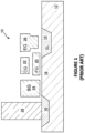
- Fig. 1 of the present application illustrates a split gate memory cell 10 with spaced apart source and drain regions 14/16 formed in a silicon semiconductor substrate 12.
- the source region 14 can be referred to as a source line SL (because it commonly is connected to other source regions for other memory cells in the same row or column), and the drain region 16 is commonly connected to a bit line by a bit line contact 28.
- a channel region 18 of the substrate is defined between the source/drain regions 14/16.
- a floating gate 20 is disposed vertically over and insulated from (and controls the conductivity of) a first portion of the channel region 18 (and partially vertically over and insulated from the source region 14).
- a control gate 22 is disposed vertically over and insulated from the floating gate 20.
- a select gate 24 is disposed vertically over and insulated from (and controls the conductivity of) a second portion of the channel region 18.
- An erase gate 26 is disposed vertically over and insulated from the source region 14 and is laterally adjacent to the floating gate 20.
- a plurality of such memory cells can be arranged in rows and columns to form a memory cell array.
- Various combinations of voltages are applied to the control gate 22, select gate 24, erase gate 26 and/or source and drain regions 14/16, to program the split gate memory cell 10 (i.e., inject electrons onto the floating gate), to erase the split gate memory cell 10 (i.e., remove electrons from the floating gate), and to read the split gate memory cell 10 (i.e., measure or detect the conductivity of the channel region 18 to determine the programming state of the floating gate 20).
- Split gate memory cell 10 can be operated in a digital manner, where the split gate memory cell 10 is set to one of only two possible states: a programmed state and an erased state.
- the split gate memory cell 10 is erased by placing a high positive voltage on the erase gate 26, and optionally a negative voltage on the control gate 22, to induce tunneling of electrons from the floating gate 20 to the erase gate 26 (leaving the floating gate 20 in a more positively charged state - the erased state).
- Split gate memory cell 10 can be programmed by placing positive voltages on the control gate 22, erase gate 26, select gate 24 and source region 14, and a current on drain region 16.
- Split gate memory cell 10 can be read by placing positive voltages on the select gate 24 (turning on the portion of channel region 18 under the select gate 24) and drain region 16 (and optionally on the erase gate 26 and/or the control gate 22), and sensing current flow through the channel region 18. If the floating gate 20 is positively charged (i.e. split gate memory cell 10 is erased), the split gate memory cell 10 will turn on, and electrical current will flow from drain region 16 to source region 14 (i.e.
- the split gate memory cell 10 is sensed to be in its erased "1" state based on sensed current flow). If the floating gate 20 is negatively charged (i.e. split gate memory cell 10 is programmed), the portion of channel region 18 under the floating gate is turned off, thereby preventing appreciable current flow (i.e., the split gate memory cell 10 is sensed to be in its programmed "0" state based on no, or minimal, current flow).
- Table 1 provides non-limiting examples of erase, program and read voltages, where Vcc is power supply voltage or another positive voltage such as 2.5 V.
- Vcc is power supply voltage or another positive voltage such as 2.5 V.
- Table 1 WL (SG) BL (Drain) Source EG CG Erase 0V 0V 0V 11.5V 0V Program 1V 1 ⁇ A 4.5V 4.5V 10.5V Read Vcc 0.6V 0V 0V Vcc
- Split gate memory cell 10 can alternately be operated in an analog manner where the memory state (i.e. the amount of charge, such as the number of electrons, on the floating gate 20) of the split gate memory cell 10 can be continuously changed anywhere from a fully erased state (minimum number of electrons on the floating gate 20) to a fully programmed state (maximum number of electrons on the floating gate 20), or just a portion of this range.
- the split gate memory cell 10 storage is analog, which allows for very precise and individual tuning of each split gate memory cell 10 in an array of split gate memory cells 10.
- the split gate memory cell 10 could be operated as an MLC (multilevel cell) where it is configured to be programmed to one of many discrete values (such as 16 or 64 different values).
- MLC multilevel cell
- the programming voltages are applied for a limited time, or as a series of pulses, until the desired programming state is achieved.
- intervening read operations between programming pulses can be used to determine if the desired programming state has been achieved (in which case programming ceases) or has not been achieved (in which case programming continues).
- Split gate memory cell 10 operated in an analog manner or as an MLC may be more sensitive to noise and read current instabilities which can adversely affect the accuracy of the split gate memory cell 10.
- One source of read current instability in analog non-volatile memory devices is the capture and emission of electrons by oxide traps located at the interface and near-interface between the gate oxide and memory cell channel region.
- the gate oxide is the insulation layer that separates the floating gate 20 from the channel region 18 of substrate 12.
- the threshold voltage Vt of the split gate memory cell 10 i.e., the minimum voltage on the control gate 22 needed to turn on the channel region 18 of the split gate memory cell 10 to produce a predetermined target current, 1 ⁇ A being an example.
- Vt the threshold voltage
- the control gate voltage is at or above the threshold voltage Vt, a conducting path is created between the source region 14 and the drain region 16, and a current of at least the predetermined target current flows.
- the control gate voltage is below the threshold voltage Vt, a conducting path is not created, and any current between the source region 14 and the drain region 16 is considered sub-threshold or leakage current.
- RTN random telegraph noise
- the instability of the split gate memory cell 10 during read can be characterized either by the threshold voltage Vt, i.e. the control gate voltage corresponding to the predetermined target current or by memory cell current under given read voltage conditions.
- the present examples are particularly described in relation to memory cell read instability as threshold voltage Vt, however the use of memory cell current under given read voltages are specifically contemplated.
- Document WO2021/045934 A1 discloses a memory device that includes a plurality of non-volatile memory cells and a controller.
- the controller is configured to erase the plurality of memory cells, program each of the memory cells, and for each of the memory cells, measure a threshold voltage applied to the memory cell corresponding to a target current through the memory cell in a first read operation, re-measure a threshold voltage applied to the memory cell corresponding to the target current through the memory cell in a second read operation, and identify the memory cell as defective if a difference between the measured threshold voltage and the re-measured threshold voltage exceeds a predetermined amount.
- Document US 8908441 B1 discloses memory cells which having read noise being identified during a programming pass and an amount of programming being increased for noisy memory cells compared to non-noisy cells.
- the read noise is indicated by a decrease in the threshold voltage of a cell when the cell is repeatedly read.
- a cell enters a temporary lockout state when it passes a first verify test and is subject to one or more additional verify tests. Data is stored to identify the cell as a noisy cell or a non-noisy cell based on the one or more additional verify tests. Or, the cells are subject to the one or more additional verify tests at the end of the programming pass.
- the noisy cell is programmed using a stricter verify condition. Or, the noisy cell is kept in an erased state.
- RTN that occurs during programming can be addressed as part of the program operation.
- one issue with RTN is that electron emission that undesirably decreases the threshold voltage Vt of the memory cell (and therefore undesirably increases channel conductivity during a read operation) can occur after programming of the memory cell is completed. Therefore, there is a need to address RTN in analog and MLC non-volatile memory devices, such as split gate memory cell 10, without limitation, to compensate for post-program RTN.
- a memory device that comprises a plurality of non-volatile memory cells each comprising a first gate, and a control circuitry.
- the control circuitry is configured to:
- the present examples illustrate a technique for compensating RTN after programming of non-volatile memory cells, such as the split gate memory cell 10 of Fig. 1 is completed, by performing post-program tuning to improve read operation accuracy.
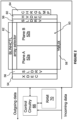
- the memory cell programming and post-program tuning techniques are implemented as part of the configuration of the control circuitry 66, which controls the various device elements for the memory array, which can be better understood from the architecture of an example memory device as illustrated in Fig. 2 .
- the memory device includes an array 50 of the split gate memory cells 10, which can be segregated into two separate planes (Plane A 52a and Plane B 52b).
- the split gate memory cells 10 can be of the type shown in Fig. 1 , arranged in a plurality of rows and columns in the semiconductor substrate 12, and thus formed on a single chip. Adjacent to the array of array 50 of split gate memory cells 10 are an address decoder (e.g. XDEC 54), source line drivers (e.g.
- SLDRV 56 SLDRV 56
- column decoder e.g. YMUX 58
- high voltage row decoder e.g. HVDEC 60
- bit line controller e.g. BLINHCTL 62
- Column decoder 58 includes a sense amplifier containing circuitry for measuring the currents on the bit lines during a read operation.
- Control circuitry 66 is configured to control the various device elements to implement each operation (program, erase, read) on selected split gate memory cells 10 of the array 50 as described herein.
- Charge pump CHRGPMP 64 provides the various voltages used to read, program and erase the selected split gate memory cells 10 of the array 50 under the control of the control circuitry 66.
- Control circuitry 66 is configured to operate the memory device to program, erase and read the selected split gate memory cells 10 of the array 50. As part of these operations, the control circuitry 66 can be provided with access to incoming data which is data to be programmed to the selected split gate memory cells 10 of the array 50, along with program, erase and read commands provided on the same or different lines. Data read from the array 50, i.e. from selected split gate memory cells 10 of the array 50. is provided as outgoing data.
- the control circuitry 66 includes, or is provided access to, a separate memory such as random access memory (RAM) 70 for storing voltage values as described further below.
- RAM random access memory
- control circuitry 66 implementing memory cell initial programming, followed by post-program tuning for memory cells that exhibit an intolerable level of read current instability after initial programming. Memory cell programming is described first, followed by post-program tuning.
- control circuitry 66 may be loaded with software, i.e. non-transitory electronically readable instructions, or firmware, to perform the methods described below in relation to Figs. 4 - 5 , thereby being configured.
- Control circuity 66 may be implemented by a microcontroller, dedicated circuitry, a processor, or a combination thereof.
- Memory cell programming involves programming a selected memory cell to an initial programming state using programming voltage pulses, with intervening read operations to measure a threshold voltage parameter (i.e., a minimum voltage applied to the split gate memory cell 10 to achieve a predetermined level of source/drain current, referred to as a target current I target ) for the memory cell.
- the threshold voltage parameter is a control gate threshold voltage Vtcg, which is the threshold voltage of the memory cell as viewed from the control gate 22 (also referred to herein as the first gate).
- control gate threshold voltage Vtcg is the voltage placed on the control gate 22 that results in the channel region 18 being a conducting path, and therefore results in a read current through the channel of the predetermined level of source/drain current, also known as the target current (I target ) (e.g., 1 ⁇ A) to consider the memory cell turned on when the read potentials of a read operation are applied to the select gate 24 and drain region 16.
- the control gate threshold voltage Vtcg varies as a function of programming state of the split gate memory cell 10, but it is desired that once the split gate memory cell 10 is programmed to a particular programming state, any variation of control gate threshold voltage Vtcg over time be below a predetermined amount.
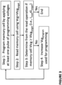
- Initial memory cell programming is illustrated as Steps 1-4 in Fig. 3 , which is implemented to program a selected split gate memory cell 10 to a specific, desired, initial programming state so that it has a target control gate threshold voltage Vtcg target that is associated with that specific, desired, initial programming state.
- the technique begins in Step 1 with control circuitry 66 programming a selected split gate memory cell 10 of array 50.
- this programming step involves applying programming voltages to the selected split gate memory cell 10 for a limited time (i.e., in at least one pulse), which results in injecting electrons onto the floating gate 20.
- the voltage Vcg applied to the control gate 22 has a control gate program voltage Vcg program value.
- Step 2 a read operation is performed which involves applying read voltages from for example SLDRV 56 to the selected split gate memory cell 10 and measuring, with column decoder 58 and bit line controller 62, the current flowing through the channel region 18 of the selected split gate memory cell 10, Iread.
- the voltage Vcg applied to the control gate 22 is the target control gate threshold voltage Vtcg target .
- Step 3 it is determined from the read operation of Step 2 whether or not the control gate threshold voltage Vtcg of the memory cell has reached or exceeded the target control gate threshold voltage Vtcg target (i.e., whether the read current I read measured by column decoder 58 and bit line controller 62 is less than or equal to the target current I target , where I read equal to the target current I target is indicative of the control gate threshold voltage Vtcg of the memory cell reaching the target control gate threshold voltage Vtcg target ).
- Read current I read for Step 3 is also referred to herein as the second read current.
- Step 4 the control gate program voltage Vcg program used for programming is increased relative to that used in the previous Step 1 programming of the memory cell, and then Step 1 is repeated using the increased control gate program voltage Vcg program .
- Steps 1-4 are repeated, in order, by control circuitry 66, until it is determined in Step 3 that the control gate threshold voltage Vtcg of the memory cell has reached or exceeded the target control gate threshold voltage Vtcg target (i.e., that the read current I read is less than or equal to the target current I target ).
- the memory cell is considered programmed to its desired, initial programming state (i.e. to its target control gate threshold voltage Vtcg target ). It is at this point where conventional programming usually ends.
- control gate threshold voltage Vtcg the control gate threshold voltage Vtcg could drop by more than ⁇ Vtcg max below the target control gate threshold voltage Vtcg target , where ⁇ Vtcg max is the maximum tolerable read error in terms of control gate threshold voltage Vtcg variation.
- a control gate threshold voltage drop by more than ⁇ Vtcg max is considered to be an intolerable error during subsequent read operations. Therefore, post-program tuning begins with Step 5 in Fig.
- the maximum control gate program voltage Vcg program value (also referred to herein as the first value) that was used in programming the memory cell (also referred to herein as the program voltage) is stored in memory (i.e., the last control gate program voltage Vcg program value used in programming the particular split gate memory cell, i.e., the last iteration of Step 4, unless the initial control gate program voltage Vcg program of Step 1 resulted in the control gate threshold voltage Vtcg of the memory cell reaching or exceeding the target control gate threshold voltage Vtcg target (i.e., that the read current I read is less than or equal to the target current I target ), in which case the initial control gate program voltage Vcg program of Step 1 is the maximum control gate program voltage Vcg program value).
- the memory used to store the maximum Vcg program value is RAM 70 if post-program tuning is performed just after analog programming.
- the maximum control gate program voltage Vcg program values can instead be stored in a file (e.g., in a non-volatile storage, accessible by control circuitry 66) to save the data for a longer period of time. Storing the maximum control gate program voltage Vcg program value is performed by control circuitry 66 after the split gate memory cell 10 is found to be programmed to its desired initial program state, as described above in relation to Step 3.
- Step 6 the split gate memory cell 10 is read (also referred to herein as a first read operation) using a control gate voltage Vcg that is less than the target control gate threshold voltage Vtcg target used in Step 2.
- the control gate voltage Vcg used for this read operation is Vtcg target - ⁇ V tcg , where ⁇ V tcg can be, but need not be, the maximum tolerable deviation of control gate threshold voltage ( ⁇ Vtcg max ).
- ⁇ V tcg max the maximum tolerable deviation of control gate threshold voltage
- ⁇ V tcg max the maximum tolerable deviation of control gate threshold voltage
- ⁇ V tcg max can be, for example, 20 mV.
- Read current I read for Step 6 is also referred to herein as the first read current. If the memory cell does not exhibit post-program intolerable RTN, then the small decrease in control gate voltage Vcg by ⁇ V tcg during the read operation of Step 6 should lower the read current I read below, or further below, I target , and the determination of Step 7 should be no, i.e. negative. In that case, the memory cell can be considered properly programmed and no post-program tuning is needed.
- Steps 6 and 7 can be repeated one or more times (where the repeated read operation is also referred to herein as a second read operation), whereby the memory cell will be subjected to another round of programming, as will be described below, if there is a positive determination in Step 7 no matter how many previous negative determinations occurred.
- Steps 6-7 even if the result in Step 7 is initially negative is advantageous because an electron may not necessarily be emitted from the trap before the first read, but could be emitted from the trap after the first read, and a yes, or positive, determination in Step 7 can occur in subsequent read operations if there is an electron emission after the first read operation.
- Step 7 the determination of Step 7 will be yes, i.e. positive, and the selected split gate memory cell 10 is subjected to another round of programming starting at Step 9, where the maximum control gate program voltage Vcg program value stored in Step 5, i.e. in RAM 70 (or other memory) is retrieved.
- the retrieved control gate program voltage Vcg program value is increased in preparation for use in programming (see Step 10) (e.g., by determining a control gate program voltage Vcg program of increased value, also referred to herein as the second value), and the determined increased control gate program voltage Vcg program value is stored in RAM 70 (or other memory) (see Step 11).
- the memory cell is then programmed in Step 12 (similar to Step 1 described above) using the increased control gate program voltage Vcg program value.
- the process then reverts back to Step 6, where the memory cell is once again read as described above with respect to Step 6, followed by the determination of Step 7 as described above. If the subsequent determination in Step 7 is yes, i.e.
- Steps 9-12 are performed again, followed by another read in Step 6 and determination in Step 7. If the subsequent determination in Step 7 is no, i.e. negative, post program tuning can end, or, steps 6-7 can be repeated one or more times as indicated in optional Step 8, even though Steps 9-12 may have been performed one or more times.
- steps 6-7 There is no limitation on the number of read and determination operations (Steps 6-7) and on the number of rounds of programming (Steps 9-12). The number of times that Steps 6-7 and 9-12 are repeated can be user defined by taking into account desired programming time.
- the post-programing tuning process can also be repeated at a time after a previous instance of post-programming tuning, in which case the increased control gate program voltage Vcg program value can be stored in a more permanent memory such as a hard drive or other non-volatile storage, accessible by control circuitry 66, for longer term storage.
- the advantage of the above described technique is that if the memory cell exhibits intolerable RTN after programming is initially completed, then it will still end up being more deeply programmed (i.e. exhibit a higher control gate threshold voltage Vtcg) than would otherwise be the case, so that the control gate threshold voltage Vtcg will not vary from the target control gate threshold voltage Vteg target by an undesired amount.
- Vtcg control gate threshold voltage
- the control gate threshold voltage Vtcg of the split gate memory cell 10 will drop below the target control gate threshold voltage Vtcg target by an amount exceeding the tolerance level of ⁇ V tcg . This is because the split gate memory cell 10 is more deeply programmed above Vtcg target and future read operations will more accurately reflect the desired programming state of the memory cell within the tolerance level of ⁇ V tcg variations.
- Fig. 5 illustrates a first alternate example, which is the same method as that described above and depicted in Figs. 3-4 , and will not be described again, except Step 6A is added before Step 6, and after Step 12 the process reverts to Step 6A instead of to Step 6.
- a negative voltage is applied to the memory cell sourced from for example SLDRV 56 under the control of control circuitry 66 (e.g. to any non-floating gate of the memory cell, such as the control gate 22, erase gate 26, and/or select gate 24), with the negative voltage defined in relation to the potential of substrate 12.
- This negative voltage applied to the split gate memory cell 10 induces electric field stress on the gate oxide of the split gate memory cell 10 to stimulate detrapping (emission) of electrons from the interface and near-interface oxide traps.
- the negative voltage is applied to the control gate 22, but it can additionally or alternatively be applied to any gate or terminal that is capacitively coupled to the floating gate 20. Therefore, for a split gate memory cell 10 that has an oxide trap which produces RTN, the negative voltage will help stimulate detrapping of electron, setting the control gate threshold voltage Vtcg to a lower threshold voltage Vt state, and increasing the chances that the determination of Step 7 will be positive (and therefore the memory cell will be subjected to additional programming).
- Step 6 Since RTN has an erratic behavior, a defective memory cell may stay in one control gate threshold voltage Vtcg state even during the read operation of Step 6, and it will therefore not be properly identified for additional programming of steps 9 - 12. Therefore, application of a negative voltage (e.g., -1 V to -7 V) before the read operation of Step 6 may stimulate a memory cell with RTN to exhibit a lower control gate threshold voltage Vtcg state and, thereby, be identified in Step 7 for additional programming, enhancing programming efficiency and accuracy. There is some characteristic time during which memory cells maintain their control gate threshold voltage Vtcg state acquired under the applied voltage stress after its removal.
- a negative voltage e.g., -1 V to -7 V
- the delay between the negative voltage application of Step 6A and the read operation of Step 6 is in one example not longer than typical electron capture and emission time (100 ms at room temperature, as an example), otherwise, application of the negative voltage of step 6A prior to the read operation of step 6 may be less efficient.
- threshold voltage Vt as viewed from any one or more gates in the split gate memory cell 10 that is not floating. Additionally, the descriptions above could be implemented in an array of memory cells with fewer gates than those in Fig. 1 (e.g., no erase gate and/or control gate combined with select gate).
Landscapes
- Engineering & Computer Science (AREA)
- Microelectronics & Electronic Packaging (AREA)
- Read Only Memory (AREA)
- Computer Hardware Design (AREA)
Claims (15)
- Speichervorrichtung, umfassend:eine Vielzahl von nichtflüchtigen Speicherzellen, jeweils umfassend ein erstes Gate; undeine Steuerschaltung, die konfiguriert ist zum:Programmieren einer ausgewählten nichtflüchtigen Speicherzelle der Vielzahl von nichtflüchtigen Speicherzellen auf einen anfänglichen Programmzustand, der einer Schwellenspannung für das erste Gate der ausgewählten nichtflüchtigen Speicherzelle entspricht, die eine Zielschwellenspannung für das erste Gate der ausgewählten nichtflüchtigen Speicherzelle erreicht oder überschreitet, wobei die Zielschwellenspannung für das erste Gate einem Ziellesestrom entspricht, wobei das Programmieren der ausgewählten nichtflüchtigen Speicherzelle ein Anlegen einer Programmspannung einschließt, die einen ersten Wert aufweist, an das erste Gate,Speichern des ersten Werts in einem Speicher,Lesen der ausgewählten nichtflüchtigen Speicherzelle in einem ersten Lesevorgang unter Verwendung einer Lesespannung, die an das erste Gate der ausgewählten nichtflüchtigen Speicherzelle angelegt wird, die kleiner als die Zielschwellenspannung für das erste Gate ist, um einen ersten Lesestrom zu erzeugen, undUnterziehen der ausgewählten nichtflüchtigen Speicherzelle dem zusätzlichen Programmieren als Reaktion auf eine Bestimmung, dass der erste Lesestrom größer als der Ziellesestrom ist, wobei das zusätzliche Programmieren umfasst:Abrufen des ersten Werts aus dem Speicher,Bestimmen eines zweiten Wertes, der größer als der erste Wert ist, undProgrammieren der ausgewählten nichtflüchtigen Speicherzelle, die ein Anlegen einer Programmspannung einschließt, die den zweiten Wert aufweist, an das erste Gate.
- Speichervorrichtung nach Anspruch 1, wobei die Steuerschaltung konfiguriert ist, um den zweiten Wert in dem Speicher zu speichern.
- Speichervorrichtung nach Anspruch 1, wobei die Steuerschaltung konfiguriert ist, um die ausgewählte nichtflüchtige Speicherzelle in den anfänglichen Programmzustand zu programmieren durch:Anlegen von mindestens einem ersten Impuls von Programmierspannungen an die ausgewählte nichtflüchtige Speicherzelle;Lesen der ausgewählten nichtflüchtigen Speicherzelle unter Verwendung einer Lesespannung, die an das erste Gate der ausgewählten nichtflüchtigen Speicherzelle angelegt wird, die gleich der Zielschwellenspannung für das erste Gate ist, um einen zweiten Lesestrom zu erzeugen; undAnlegen von mindestens einem zweiten Impuls von Programmierspannungen an die ausgewählte nichtflüchtige Speicherzelle als Reaktion auf eine Bestimmung, dass der zweite Lesestrom nicht kleiner als oder gleich des Ziellesestroms ist.
- Speichervorrichtung nach Anspruch 1, wobei die Steuerschaltung konfiguriert ist zum:Lesen der ausgewählten nichtflüchtigen Speicherzelle in einem zweiten durchgeführten Lesevorgang als Reaktion auf eine Bestimmung, dass der erste Lesestrom nicht größer als der Ziellesestrom in dem ersten Lesevorgang ist, unter Verwendung einer Lesespannung, die an das erste Gate der ausgewählten nichtflüchtigen Speicherzelle angelegt wird, die kleiner als die Zielschwellenspannung ist, um einen zweiten Lesestrom zu erzeugen, undUnterziehen der ausgewählten nichtflüchtigen Speicherzelle dem zusätzlichen Programmieren als Reaktion auf eine Bestimmung, dass der zweite Lesestrom größer als der Ziellesestrom ist; undnicht Unterziehen der ausgewählten nichtflüchtigen Speicherzelle dem zusätzlichen Programmieren als Reaktion auf eine Bestimmung, dass der zweite Lesestrom nicht größer als der Ziellesestrom ist.
- Speichervorrichtung nach Anspruch 1, wobei die Steuerschaltung konfiguriert ist, um nach dem Programmieren der ausgewählten nichtflüchtigen Speicherzelle in den anfänglichen Programmzustand und vor dem ersten Lesevorgang eine negative Spannung an ein Non-Floating-Gate der ausgewählten nichtflüchtigen Speicherzelle anzulegen, und/oder
wobei die Steuerschaltung konfiguriert ist, um nach dem Programmieren der ausgewählten nichtflüchtigen Speicherzelle in den anfänglichen Programmzustand und vor dem ersten Lesevorgang eine negative Spannung an das erste Gate der ausgewählten nichtflüchtigen Speicherzelle anzulegen. - Speichervorrichtung nach Anspruch 4, wobei die Steuerschaltung ferner konfiguriert ist zum:Anlegen einer negativen Spannung an das erste Gate der ausgewählten nichtflüchtigen Speicherzelle nach dem Programmieren der ausgewählten nichtflüchtigen Speicherzelle in den anfänglichen Programmzustand und vor dem ersten Lesevorgang; undAnlegen einer negativen Spannung an das erste Gate der ausgewählten nichtflüchtigen Speicherzelle nach dem Bestimmen, dass der erste Lesestrom nicht größer als der Ziellesestrom in dem ersten Lesevorgang und vor dem zweiten Lesevorgang ist.
- Verfahren zum Programmieren einer ausgewählten nichtflüchtigen Speicherzelle aus einer Vielzahl von nichtflüchtigen Speicherzellen, wobei jede der Vielzahl von nichtflüchtigen Speicherzellen ein erstes Gate einschließt, das Verfahren umfassend:Programmieren der ausgewählten nichtflüchtigen Speicherzelle in einen anfänglichen Programmzustand, der dem Erreichen oder dem Überschreiten einer Zielschwellenspannung für das erste Gate der ausgewählten nichtflüchtigen Speicherzelle entspricht, wobei die Zielschwellenspannung einem Ziellesestrom entspricht, wobei das Programmieren das Anlegen einer Programmspannung einschließt, die einen ersten Wert aufweist, an das erste Gate,Speichern des ersten Wertes in einem Speicher,Lesen der ausgewählten nichtflüchtigen Speicherzelle in einem ersten Lesevorgang unter Verwendung einer Lesespannung, die an das erste Gate der einen nichtflüchtigen Speicherzelle angelegt wird, die kleiner als die Zielschwellenspannung ist, um den ausgewählten ersten Lesestrom zu erzeugen, undUnterziehen der ausgewählten nichtflüchtigen Speicherzelle dem zusätzlichen Programmieren als Reaktion auf ein Bestimmen, dass der erste Lesestrom größer als der Ziellesestrom ist, wobei das zusätzliche Programmieren umfasst:Abrufen des ersten Wertes aus dem Speicher,Bestimmen eines zweiten Werts, der größer als der erste Wert ist, undProgrammieren der ausgewählten nichtflüchtigen Speicherzelle, das das Anlegen einer Programmspannung einschließt, die den zweiten Wert an das erste Gate aufweist.
- Verfahren nach Anspruch 7, umfassend:
Speichern des zweiten Werts in dem Speicher. - Speichervorrichtung nach Anspruch 1 oder Verfahren nach Anspruch 7, wobei jede der Vielzahl von nichtflüchtigen Speicherzellen ferner umfasst:voneinander beabstandete Source- und Drain-Regionen, die in einem Halbleitersubstrat ausgebildet sind, wobei sich eine Kanalregion des Substrats dazwischen erstreckt;ein Floating-Gate, das über einem ersten Abschnitt der Kanalregion vertikal angeordnet und von diesem isoliert ist; undein Auswahl-Gate, das über einem zweiten Abschnitt der Kanalregion vertikal angeordnet und von diesem isoliert ist;wobei für jede der Vielzahl von nichtflüchtigen Speicherzellen das erste Gate über dem Floating-Gate vertikal angeordnet und von diesem isoliert ist.
- Speichervorrichtung nach Anspruch 1 oder Verfahren nach Anspruch 9, wobei jede der Vielzahl von nichtflüchtigen Speicherzellen ferner umfasst:
ein Lösch-Gate, das über der Source-Region angeordnet und von dieser isoliert ist. - Verfahren nach Anspruch 7, wobei das Programmieren der ausgewählten nichtflüchtigen Speicherzelle in den anfänglichen Programmzustand umfasst:Anlegen von mindestens einem ersten Impuls von Programmierspannungen an die eine nichtflüchtige Speicherzelle;Lesen der ausgewählten nichtflüchtigen Speicherzelle unter Verwendung einer Lesespannung, die an das erste Gate der ausgewählten nichtflüchtigen Speicherzelle angelegt wird, die gleich der Zielschwellenspannung ist, um einen zweiten Lesestrom zu erzeugen; undAnlegen von mindestens einem zweiten Impuls von Programmierspannungen an die ausgewählte nichtflüchtige Speicherzelle als Reaktion auf das Bestimmen, dass der zweite Lesestrom größer als der Ziellesestrom ist.
- Speichervorrichtung nach Anspruch 3 oder Verfahren nach Anspruch 11, wobei der mindestens eine erste Impuls von Programmspannungen eine erste Programmspannung einschließt, die an das erste Gate angelegt wird, und der mindestens eine zweite Impuls von Programmierspannungen eine zweite Programmspannung einschließt, die an das erste Gate angelegt wird und die größer als die erste Programmspannung ist.
- Verfahren nach Anspruch 7, umfassend:Lesen der ausgewählten nichtflüchtigen Speicherzelle in einem zweiten durchgeführten Lesevorgang als Reaktion auf das Bestimmen, dass der erste Lesestrom nicht größer als der Ziellesestrom in dem ersten Lesevorgang ist, unter Verwendung einer Lesespannung, die an das erste Gate der ausgewählten nichtflüchtigen Speicherzelle angelegt wird, die kleiner als die Zielschwellenspannung ist, um einen zweiten Lesestrom zu erzeugen, undUnterziehen der ausgewählten nichtflüchtigen Speicherzelle dem zusätzlichen Programmieren als Reaktion auf das Bestimmen, dass der zweite Lesestrom größer als der Ziellesestrom ist; undnicht Unterziehen der ausgewählten nichtflüchtigen Speicherzelle dem zusätzlichen Programmieren als Reaktion auf das Bestimmen, dass der zweite Lesestrom größer als der Ziellesestrom ist.
- Verfahren nach Anspruch 7, ferner umfassend:Anlegen einer negativen Spannung an das Non-Floating-Gate der ausgewählten nichtflüchtigen Speicherzelle nach dem Programmieren der ausgewählten nichtflüchtigen Speicherzelle in den anfänglichen Programmzustand und vor dem ersten Lesevorgang, und/oderferner umfassend:
Anlegen einer negativen Spannung an das erste Gate der ausgewählten nichtflüchtigen Speicherzelle nach dem Programmieren der ausgewählten nichtflüchtigen Speicherzelle in den anfänglichen Programmzustand und vor dem ersten Lesevorgang. - Verfahren nach Anspruch 13, umfassend:Anlegen einer negativen Spannung an das erste Gate der ausgewählten nichtflüchtigen Speicherzelle nach dem Programmieren der ausgewählten nichtflüchtigen Speicherzelle in den anfänglichen Programmzustand und vor dem ersten Lesevorgang; undAnlegen einer negativen Spannung an das erste Gate der ausgewählten nichtflüchtigen Speicherzelle nach dem Bestimmen, dass der erste Lesestrom nicht größer als der Ziellesestrom in dem ersten Lesevorgang und vor dem zweiten Lesevorgang ist.
Applications Claiming Priority (3)
| Application Number | Priority Date | Filing Date | Title |
|---|---|---|---|
| US202163196130P | 2021-06-02 | 2021-06-02 | |
| US17/481,225 US12080355B2 (en) | 2021-06-02 | 2021-09-21 | Method of improving read current stability in analog non-volatile memory by post-program tuning for memory cells exhibiting random telegraph noise |
| PCT/US2021/052234 WO2022256030A1 (en) | 2021-06-02 | 2021-09-27 | Method of improving read current stability in analog non-volatile memory by post-program tuning for memory cells exhibiting random telegraph noise |
Publications (2)
| Publication Number | Publication Date |
|---|---|
| EP4348651A1 EP4348651A1 (de) | 2024-04-10 |
| EP4348651B1 true EP4348651B1 (de) | 2025-04-02 |
Family
ID=78302995
Family Applications (1)
| Application Number | Title | Priority Date | Filing Date |
|---|---|---|---|
| EP21795151.6A Active EP4348651B1 (de) | 2021-06-02 | 2021-09-27 | Verfahren zur verbesserung der lesestromstabilität in einem analogen nichtflüchtigen speicher durch nachprogrammierungsabstimmung von speicherzellen mit zufälligem telegrafischem rauschen |
Country Status (5)
| Country | Link |
|---|---|
| EP (1) | EP4348651B1 (de) |
| JP (1) | JP7628629B2 (de) |
| KR (1) | KR102839068B1 (de) |
| TW (1) | TWI832254B (de) |
| WO (1) | WO2022256030A1 (de) |
Families Citing this family (1)
| Publication number | Priority date | Publication date | Assignee | Title |
|---|---|---|---|---|
| CN116597881A (zh) * | 2023-05-31 | 2023-08-15 | 上海华虹宏力半导体制造有限公司 | 闪存及其编程电压控制方法 |
Family Cites Families (10)
| Publication number | Priority date | Publication date | Assignee | Title |
|---|---|---|---|---|
| US6222762B1 (en) * | 1992-01-14 | 2001-04-24 | Sandisk Corporation | Multi-state memory |
| DE102005009700B4 (de) * | 2004-02-26 | 2009-02-05 | Samsung Electronics Co., Ltd., Suwon | Programmierverfahren und nichtflüchtiger Speicher |
| US20090039410A1 (en) | 2007-08-06 | 2009-02-12 | Xian Liu | Split Gate Non-Volatile Flash Memory Cell Having A Floating Gate, Control Gate, Select Gate And An Erase Gate With An Overhang Over The Floating Gate, Array And Method Of Manufacturing |
| JP2009266356A (ja) * | 2008-04-30 | 2009-11-12 | Toshiba Corp | Nand型フラッシュメモリ |
| US7957190B2 (en) | 2008-05-30 | 2011-06-07 | Freescale Semiconductor, Inc. | Memory having P-type split gate memory cells and method of operation |
| US8908441B1 (en) * | 2013-10-15 | 2014-12-09 | Sandisk Technologies Inc. | Double verify method in multi-pass programming to suppress read noise |
| JP5868381B2 (ja) * | 2013-12-03 | 2016-02-24 | ウィンボンド エレクトロニクス コーポレーション | 半導体記憶装置 |
| KR102182583B1 (ko) * | 2016-05-17 | 2020-11-24 | 실리콘 스토리지 테크놀로지 인크 | 비휘발성 메모리 어레이를 사용하는 딥러닝 신경망 분류기 |
| US11449741B2 (en) * | 2019-07-19 | 2022-09-20 | Silicon Storage Technology, Inc. | Testing circuitry and methods for analog neural memory in artificial neural network |
| US11017866B2 (en) * | 2019-09-03 | 2021-05-25 | Silicon Storage Technology, Inc. | Method of improving read current stability in analog non-volatile memory using final bake in predetermined program state |
-
2021
- 2021-09-27 WO PCT/US2021/052234 patent/WO2022256030A1/en not_active Ceased
- 2021-09-27 KR KR1020237039958A patent/KR102839068B1/ko active Active
- 2021-09-27 JP JP2023565896A patent/JP7628629B2/ja active Active
- 2021-09-27 EP EP21795151.6A patent/EP4348651B1/de active Active
-
2022
- 2022-05-23 TW TW111119037A patent/TWI832254B/zh active
Also Published As
| Publication number | Publication date |
|---|---|
| JP7628629B2 (ja) | 2025-02-10 |
| KR20230172027A (ko) | 2023-12-21 |
| EP4348651A1 (de) | 2024-04-10 |
| TW202314724A (zh) | 2023-04-01 |
| KR102839068B1 (ko) | 2025-07-28 |
| TWI832254B (zh) | 2024-02-11 |
| WO2022256030A1 (en) | 2022-12-08 |
| JP2024520275A (ja) | 2024-05-24 |
Similar Documents
| Publication | Publication Date | Title |
|---|---|---|
| US11017866B2 (en) | Method of improving read current stability in analog non-volatile memory using final bake in predetermined program state | |
| US11309042B2 (en) | Method of improving read current stability in analog non-volatile memory by program adjustment for memory cells exhibiting random telegraph noise | |
| EP4352728B1 (de) | Verfahren zur reduzierung von zufälligem telegrafischem rauschen in einem nichtflüchtigen speicher durch gruppierung und screening von speicherzellen | |
| EP4348651B1 (de) | Verfahren zur verbesserung der lesestromstabilität in einem analogen nichtflüchtigen speicher durch nachprogrammierungsabstimmung von speicherzellen mit zufälligem telegrafischem rauschen | |
| US12080355B2 (en) | Method of improving read current stability in analog non-volatile memory by post-program tuning for memory cells exhibiting random telegraph noise | |
| CN117321689A (zh) | 通过对表现出随机电报噪声的存储器单元进行编程后调谐来提高模拟非易失性存储器中的读取电流稳定性的方法 | |
| WO2022260692A1 (en) | Method of reducing random telegraph noise in non-volatile memory by grouping and screening memory cells |
Legal Events
| Date | Code | Title | Description |
|---|---|---|---|
| STAA | Information on the status of an ep patent application or granted ep patent |
Free format text: STATUS: UNKNOWN |
|
| STAA | Information on the status of an ep patent application or granted ep patent |
Free format text: STATUS: THE INTERNATIONAL PUBLICATION HAS BEEN MADE |
|
| PUAI | Public reference made under article 153(3) epc to a published international application that has entered the european phase |
Free format text: ORIGINAL CODE: 0009012 |
|
| STAA | Information on the status of an ep patent application or granted ep patent |
Free format text: STATUS: REQUEST FOR EXAMINATION WAS MADE |
|
| 17P | Request for examination filed |
Effective date: 20231220 |
|
| AK | Designated contracting states |
Kind code of ref document: A1 Designated state(s): AL AT BE BG CH CY CZ DE DK EE ES FI FR GB GR HR HU IE IS IT LI LT LU LV MC MK MT NL NO PL PT RO RS SE SI SK SM TR |
|
| DAV | Request for validation of the european patent (deleted) | ||
| DAX | Request for extension of the european patent (deleted) | ||
| GRAP | Despatch of communication of intention to grant a patent |
Free format text: ORIGINAL CODE: EPIDOSNIGR1 |
|
| STAA | Information on the status of an ep patent application or granted ep patent |
Free format text: STATUS: GRANT OF PATENT IS INTENDED |
|
| RIC1 | Information provided on ipc code assigned before grant |
Ipc: G11C 11/56 20060101ALN20240924BHEP Ipc: G11C 16/34 20060101ALI20240924BHEP Ipc: G11C 16/10 20060101ALI20240924BHEP Ipc: G11C 16/04 20060101AFI20240924BHEP |
|
| RAP3 | Party data changed (applicant data changed or rights of an application transferred) |
Owner name: SILICON STORAGE TECHNOLOGY, INC. |
|
| INTG | Intention to grant announced |
Effective date: 20241023 |
|
| GRAS | Grant fee paid |
Free format text: ORIGINAL CODE: EPIDOSNIGR3 |
|
| GRAA | (expected) grant |
Free format text: ORIGINAL CODE: 0009210 |
|
| STAA | Information on the status of an ep patent application or granted ep patent |
Free format text: STATUS: THE PATENT HAS BEEN GRANTED |
|
| AK | Designated contracting states |
Kind code of ref document: B1 Designated state(s): AL AT BE BG CH CY CZ DE DK EE ES FI FR GB GR HR HU IE IS IT LI LT LU LV MC MK MT NL NO PL PT RO RS SE SI SK SM TR |
|
| P01 | Opt-out of the competence of the unified patent court (upc) registered |
Free format text: CASE NUMBER: APP_9108/2025 Effective date: 20250224 |
|
| REG | Reference to a national code |
Ref country code: GB Ref legal event code: FG4D |
|
| REG | Reference to a national code |
Ref country code: CH Ref legal event code: EP |
|
| REG | Reference to a national code |
Ref country code: IE Ref legal event code: FG4D |
|
| REG | Reference to a national code |
Ref country code: DE Ref legal event code: R096 Ref document number: 602021028615 Country of ref document: DE |
|
| REG | Reference to a national code |
Ref country code: NL Ref legal event code: FP |
|
| PGFP | Annual fee paid to national office [announced via postgrant information from national office to epo] |
Ref country code: NL Payment date: 20250820 Year of fee payment: 5 |
|
| REG | Reference to a national code |
Ref country code: AT Ref legal event code: MK05 Ref document number: 1782124 Country of ref document: AT Kind code of ref document: T Effective date: 20250402 |
|
| PG25 | Lapsed in a contracting state [announced via postgrant information from national office to epo] |
Ref country code: FI Free format text: LAPSE BECAUSE OF FAILURE TO SUBMIT A TRANSLATION OF THE DESCRIPTION OR TO PAY THE FEE WITHIN THE PRESCRIBED TIME-LIMIT Effective date: 20250402 Ref country code: ES Free format text: LAPSE BECAUSE OF FAILURE TO SUBMIT A TRANSLATION OF THE DESCRIPTION OR TO PAY THE FEE WITHIN THE PRESCRIBED TIME-LIMIT Effective date: 20250402 Ref country code: PT Free format text: LAPSE BECAUSE OF FAILURE TO SUBMIT A TRANSLATION OF THE DESCRIPTION OR TO PAY THE FEE WITHIN THE PRESCRIBED TIME-LIMIT Effective date: 20250804 |
|
| PGFP | Annual fee paid to national office [announced via postgrant information from national office to epo] |
Ref country code: DE Payment date: 20250820 Year of fee payment: 5 |
|
| REG | Reference to a national code |
Ref country code: LT Ref legal event code: MG9D |
|
| PG25 | Lapsed in a contracting state [announced via postgrant information from national office to epo] |
Ref country code: NO Free format text: LAPSE BECAUSE OF FAILURE TO SUBMIT A TRANSLATION OF THE DESCRIPTION OR TO PAY THE FEE WITHIN THE PRESCRIBED TIME-LIMIT Effective date: 20250702 Ref country code: GR Free format text: LAPSE BECAUSE OF FAILURE TO SUBMIT A TRANSLATION OF THE DESCRIPTION OR TO PAY THE FEE WITHIN THE PRESCRIBED TIME-LIMIT Effective date: 20250703 |
|
| PG25 | Lapsed in a contracting state [announced via postgrant information from national office to epo] |
Ref country code: PL Free format text: LAPSE BECAUSE OF FAILURE TO SUBMIT A TRANSLATION OF THE DESCRIPTION OR TO PAY THE FEE WITHIN THE PRESCRIBED TIME-LIMIT Effective date: 20250402 |
|
| PG25 | Lapsed in a contracting state [announced via postgrant information from national office to epo] |
Ref country code: BG Free format text: LAPSE BECAUSE OF FAILURE TO SUBMIT A TRANSLATION OF THE DESCRIPTION OR TO PAY THE FEE WITHIN THE PRESCRIBED TIME-LIMIT Effective date: 20250402 |
|
| PG25 | Lapsed in a contracting state [announced via postgrant information from national office to epo] |
Ref country code: HR Free format text: LAPSE BECAUSE OF FAILURE TO SUBMIT A TRANSLATION OF THE DESCRIPTION OR TO PAY THE FEE WITHIN THE PRESCRIBED TIME-LIMIT Effective date: 20250402 |
|
| PG25 | Lapsed in a contracting state [announced via postgrant information from national office to epo] |
Ref country code: AT Free format text: LAPSE BECAUSE OF FAILURE TO SUBMIT A TRANSLATION OF THE DESCRIPTION OR TO PAY THE FEE WITHIN THE PRESCRIBED TIME-LIMIT Effective date: 20250402 |
|
| PGFP | Annual fee paid to national office [announced via postgrant information from national office to epo] |
Ref country code: FR Payment date: 20250821 Year of fee payment: 5 |
|
| PG25 | Lapsed in a contracting state [announced via postgrant information from national office to epo] |
Ref country code: RS Free format text: LAPSE BECAUSE OF FAILURE TO SUBMIT A TRANSLATION OF THE DESCRIPTION OR TO PAY THE FEE WITHIN THE PRESCRIBED TIME-LIMIT Effective date: 20250702 |
|
| PG25 | Lapsed in a contracting state [announced via postgrant information from national office to epo] |
Ref country code: IS Free format text: LAPSE BECAUSE OF FAILURE TO SUBMIT A TRANSLATION OF THE DESCRIPTION OR TO PAY THE FEE WITHIN THE PRESCRIBED TIME-LIMIT Effective date: 20250802 |
|
| PG25 | Lapsed in a contracting state [announced via postgrant information from national office to epo] |
Ref country code: LV Free format text: LAPSE BECAUSE OF FAILURE TO SUBMIT A TRANSLATION OF THE DESCRIPTION OR TO PAY THE FEE WITHIN THE PRESCRIBED TIME-LIMIT Effective date: 20250402 |
|
| PG25 | Lapsed in a contracting state [announced via postgrant information from national office to epo] |
Ref country code: DK Free format text: LAPSE BECAUSE OF FAILURE TO SUBMIT A TRANSLATION OF THE DESCRIPTION OR TO PAY THE FEE WITHIN THE PRESCRIBED TIME-LIMIT Effective date: 20250402 Ref country code: SM Free format text: LAPSE BECAUSE OF FAILURE TO SUBMIT A TRANSLATION OF THE DESCRIPTION OR TO PAY THE FEE WITHIN THE PRESCRIBED TIME-LIMIT Effective date: 20250402 |
|
| PG25 | Lapsed in a contracting state [announced via postgrant information from national office to epo] |
Ref country code: CZ Free format text: LAPSE BECAUSE OF FAILURE TO SUBMIT A TRANSLATION OF THE DESCRIPTION OR TO PAY THE FEE WITHIN THE PRESCRIBED TIME-LIMIT Effective date: 20250402 |
|
| PG25 | Lapsed in a contracting state [announced via postgrant information from national office to epo] |
Ref country code: EE Free format text: LAPSE BECAUSE OF FAILURE TO SUBMIT A TRANSLATION OF THE DESCRIPTION OR TO PAY THE FEE WITHIN THE PRESCRIBED TIME-LIMIT Effective date: 20250402 |
|
| PG25 | Lapsed in a contracting state [announced via postgrant information from national office to epo] |
Ref country code: SK Free format text: LAPSE BECAUSE OF FAILURE TO SUBMIT A TRANSLATION OF THE DESCRIPTION OR TO PAY THE FEE WITHIN THE PRESCRIBED TIME-LIMIT Effective date: 20250402 |
|
| PG25 | Lapsed in a contracting state [announced via postgrant information from national office to epo] |
Ref country code: IT Free format text: LAPSE BECAUSE OF FAILURE TO SUBMIT A TRANSLATION OF THE DESCRIPTION OR TO PAY THE FEE WITHIN THE PRESCRIBED TIME-LIMIT Effective date: 20250402 |
|
| PLBE | No opposition filed within time limit |
Free format text: ORIGINAL CODE: 0009261 |
|
| STAA | Information on the status of an ep patent application or granted ep patent |
Free format text: STATUS: NO OPPOSITION FILED WITHIN TIME LIMIT |
|
| REG | Reference to a national code |
Ref country code: CH Ref legal event code: L10 Free format text: ST27 STATUS EVENT CODE: U-0-0-L10-L00 (AS PROVIDED BY THE NATIONAL OFFICE) Effective date: 20260211 |