EP4372829A2 - Solarzelle, herstellungsverfahren dafür und photovoltaisches modul - Google Patents
Solarzelle, herstellungsverfahren dafür und photovoltaisches modul Download PDFInfo
- Publication number
- EP4372829A2 EP4372829A2 EP24168316.8A EP24168316A EP4372829A2 EP 4372829 A2 EP4372829 A2 EP 4372829A2 EP 24168316 A EP24168316 A EP 24168316A EP 4372829 A2 EP4372829 A2 EP 4372829A2
- Authority
- EP
- European Patent Office
- Prior art keywords
- layer
- oxide layer
- solar cell
- semiconductor substrate
- substructure
- Prior art date
- Legal status (The legal status is an assumption and is not a legal conclusion. Google has not performed a legal analysis and makes no representation as to the accuracy of the status listed.)
- Granted
Links
Images


Classifications
-
- H—ELECTRICITY
- H10—SEMICONDUCTOR DEVICES; ELECTRIC SOLID-STATE DEVICES NOT OTHERWISE PROVIDED FOR
- H10F—INORGANIC SEMICONDUCTOR DEVICES SENSITIVE TO INFRARED RADIATION, LIGHT, ELECTROMAGNETIC RADIATION OF SHORTER WAVELENGTH OR CORPUSCULAR RADIATION
- H10F77/00—Constructional details of devices covered by this subclass
- H10F77/30—Coatings
- H10F77/306—Coatings for devices having potential barriers
- H10F77/311—Coatings for devices having potential barriers for photovoltaic cells
-
- H—ELECTRICITY
- H10—SEMICONDUCTOR DEVICES; ELECTRIC SOLID-STATE DEVICES NOT OTHERWISE PROVIDED FOR
- H10F—INORGANIC SEMICONDUCTOR DEVICES SENSITIVE TO INFRARED RADIATION, LIGHT, ELECTROMAGNETIC RADIATION OF SHORTER WAVELENGTH OR CORPUSCULAR RADIATION
- H10F10/00—Individual photovoltaic cells, e.g. solar cells
- H10F10/10—Individual photovoltaic cells, e.g. solar cells having potential barriers
- H10F10/14—Photovoltaic cells having only PN homojunction potential barriers
-
- H—ELECTRICITY
- H10—SEMICONDUCTOR DEVICES; ELECTRIC SOLID-STATE DEVICES NOT OTHERWISE PROVIDED FOR
- H10F—INORGANIC SEMICONDUCTOR DEVICES SENSITIVE TO INFRARED RADIATION, LIGHT, ELECTROMAGNETIC RADIATION OF SHORTER WAVELENGTH OR CORPUSCULAR RADIATION
- H10F71/00—Manufacture or treatment of devices covered by this subclass
- H10F71/121—The active layers comprising only Group IV materials
- H10F71/1224—The active layers comprising only Group IV materials comprising microcrystalline silicon
-
- H—ELECTRICITY
- H10—SEMICONDUCTOR DEVICES; ELECTRIC SOLID-STATE DEVICES NOT OTHERWISE PROVIDED FOR
- H10F—INORGANIC SEMICONDUCTOR DEVICES SENSITIVE TO INFRARED RADIATION, LIGHT, ELECTROMAGNETIC RADIATION OF SHORTER WAVELENGTH OR CORPUSCULAR RADIATION
- H10F71/00—Manufacture or treatment of devices covered by this subclass
- H10F71/129—Passivating
-
- H—ELECTRICITY
- H10—SEMICONDUCTOR DEVICES; ELECTRIC SOLID-STATE DEVICES NOT OTHERWISE PROVIDED FOR
- H10F—INORGANIC SEMICONDUCTOR DEVICES SENSITIVE TO INFRARED RADIATION, LIGHT, ELECTROMAGNETIC RADIATION OF SHORTER WAVELENGTH OR CORPUSCULAR RADIATION
- H10F77/00—Constructional details of devices covered by this subclass
- H10F77/10—Semiconductor bodies
- H10F77/16—Material structures, e.g. crystalline structures, film structures or crystal plane orientations
- H10F77/162—Non-monocrystalline materials, e.g. semiconductor particles embedded in insulating materials
- H10F77/164—Polycrystalline semiconductors
- H10F77/1642—Polycrystalline semiconductors including only Group IV materials
- H10F77/1645—Polycrystalline semiconductors including only Group IV materials including microcrystalline silicon
-
- H—ELECTRICITY
- H10—SEMICONDUCTOR DEVICES; ELECTRIC SOLID-STATE DEVICES NOT OTHERWISE PROVIDED FOR
- H10F—INORGANIC SEMICONDUCTOR DEVICES SENSITIVE TO INFRARED RADIATION, LIGHT, ELECTROMAGNETIC RADIATION OF SHORTER WAVELENGTH OR CORPUSCULAR RADIATION
- H10F77/00—Constructional details of devices covered by this subclass
- H10F77/70—Surface textures, e.g. pyramid structures
- H10F77/703—Surface textures, e.g. pyramid structures of the semiconductor bodies, e.g. textured active layers
-
- H—ELECTRICITY
- H10—SEMICONDUCTOR DEVICES; ELECTRIC SOLID-STATE DEVICES NOT OTHERWISE PROVIDED FOR
- H10F—INORGANIC SEMICONDUCTOR DEVICES SENSITIVE TO INFRARED RADIATION, LIGHT, ELECTROMAGNETIC RADIATION OF SHORTER WAVELENGTH OR CORPUSCULAR RADIATION
- H10F77/00—Constructional details of devices covered by this subclass
- H10F77/70—Surface textures, e.g. pyramid structures
- H10F77/707—Surface textures, e.g. pyramid structures of the substrates or of layers on substrates, e.g. textured ITO layer on a glass substrate
-
- Y—GENERAL TAGGING OF NEW TECHNOLOGICAL DEVELOPMENTS; GENERAL TAGGING OF CROSS-SECTIONAL TECHNOLOGIES SPANNING OVER SEVERAL SECTIONS OF THE IPC; TECHNICAL SUBJECTS COVERED BY FORMER USPC CROSS-REFERENCE ART COLLECTIONS [XRACs] AND DIGESTS
- Y02—TECHNOLOGIES OR APPLICATIONS FOR MITIGATION OR ADAPTATION AGAINST CLIMATE CHANGE
- Y02P—CLIMATE CHANGE MITIGATION TECHNOLOGIES IN THE PRODUCTION OR PROCESSING OF GOODS
- Y02P70/00—Climate change mitigation technologies in the production process for final industrial or consumer products
- Y02P70/50—Manufacturing or production processes characterised by the final manufactured product
Definitions
- the present disclosure relates to the field of photovoltaic cell technologies, and in particular, to a solar cell, a manufacturing method thereof, and a photovoltaic module.
- An N-type tunnel oxide passivated contact (TOPCon) solar cell relies on a "tunnel effect" to achieve passivated contact on a rear surface of the solar cell.
- borosilicate glass is formed by boron diffusion on a surface of a silicon wafer (or a substrate), which is more difficult to be removed compared with phosphorosilicate glass of a conventional PERC solar cell.
- borosilicate glass on a rear surface of an N-type solar cell is removed by an oxidizing mixed acid solution. After the surface is cleaned and dried, the rear surface is polished with the aid of a trough or chain acid additive.
- the polished rear surface of the silicon wafer has a flat structure, but the structure of the polished rear surface may directly affect the manufacturing of the tunnel oxide layer and the polycrystalline silicon layer, and then affect passivation performance and conversion efficiency of the solar cell.
- the present disclosure provides a solar cell, a manufacturing method thereof, and a photovoltaic module, which, through matching between texture structures on substrate surfaces of the solar cell, can improve an open-circuit voltage of the solar cell, reduce contact resistance of a metal electrode, and improve conversion efficiency of the solar cell.
- the present disclosure provides a solar cell, including:
- the front surface of the semiconductor substrate has a second texture structure
- the second texture structure includes a pyramid-shaped microstructure
- the pyramid-shaped microstructure includes a top portion away from the front surface of the semiconductor substrate and a bottom portion close to the front surface of the semiconductor substrate, and in a direction away from the front surface and perpendicular to the front surface, a distance between the top portion and the bottom portion of the pyramid-shaped microstructure is less than or equal to 5 ⁇ m.
- the distance between the top surface of the outermost first substructure and the top surface of the adjacent first substructure ranges from 0.3 ⁇ m to 1.2 ⁇ m.
- an average one-dimensional size of the top surface of the outermost first substructure ranges from 10 ⁇ m to 15 ⁇ m.
- a thickness of the tunnel oxide layer on the top surface of the outermost first substructure is less than a thickness of the tunnel oxide layer on a side surface of the outermost first substructure.
- a thickness difference between the tunnel oxide layer on the top surface of the outermost first substructure and the tunnel oxide layer on a side surface of the outermost first substructure is less than or equal to 0.15 nm.
- the first texture structure further includes two or more adjacent second substructures that do not stacked on one another, and a one-dimensional size of a top surface of the second substructure away from the rear surface is less than or equal to 45 ⁇ m.
- the top surface of the first substructure and/or the top surface of the second substructure is a polygonal plane.
- a shape of the polygonal plane includes at least one of a diamond, a square, a trapezoid, a substantially diamond, a substantially square or a substantially trapezoid.
- the tunnel oxide layer includes at least one of a silicon oxide layer, an aluminum oxide layer, a silicon oxynitride layer, a molybdenum oxide layer or a hafnium oxide layer, and the tunnel oxide layer has a thickness ranging from 0.8 nm to 2 nm.
- the second passivation layer includes at least one of a silicon nitride layer, a silicon oxide layer or a silicon oxynitride layer, and the second passivation layer has a thickness ranging from 70 nm to 120 nm.
- the first passivation layer includes at least one of a silicon oxide layer, a silicon nitride layer, an aluminum oxide layer or a silicon oxynitride layer.
- the semiconductor substrate is an N-type monocrystalline silicon substrate
- the doped conductive layer is an N-type doped polycrystalline silicon layer, an N-type doped microcrystalline silicon layer or an N-type doped amorphous silicon layer
- the doped conductive layer has a thickness ranging from 60 nm to 200 nm.
- the present disclosure provides a photovoltaic module, including a plurality of solar cell strings, each of the plurality of solar cell strings including the solar cell described in the first aspect.
- the present disclosure provides a method for manufacturing a solar cell, including:
- the polishing a rear surface of the semiconductor substrate with an alkali solution includes: cleaning the rear surface of the semiconductor substrate with the alkali solution having a mass fraction of 5% to 15% to remove porous silicon; dropping, by spraying, micro-liquid droplets of the alkali solution to the rear surface of the semiconductor substrate for roughening treatment, and then performing pre-cleaning with a hydrofluoric acid having a mass fraction of 5% to 10%; polishing the rear surface of the semiconductor substrate with a polishing liquid at a polishing temperature ranging from 70°C to 80°C for a polishing time less than 260 seconds, wherein the polishing liquid includes NaOH having a mass fraction of 1% to 15%, KOH having a mass fraction of 1% to 15% and an additive having a mass fraction of 0.51% to 2.5%; removing organic components in the polishing liquid by a mixture of potassium hydroxide having a mass fraction of 5% to 15% and hydrogen peroxide having a mass fraction of 15% to 40%; and washing and drying the polished semiconductor substrate.
- the forming a tunnel oxide layer includes at least one of (1) depositing the tunnel oxide layer on the first texture structure of the rear surface of the semiconductor substrate by a temperature change process and chemical vapor deposition; (2) during the deposition of the tunnel oxide layer, controlling a heating rate to range from 0.5°C/min to 3°C/min, a deposition temperature to range from 560°C to 620°C and a deposition time to range from 3 min to 10 min; (3) a deposition temperature of the tunnel oxide layer being lower than a deposition temperature of the polycrystalline silicon layer; (4) the tunnel oxide layer including at least one of a silicon oxide layer, an aluminum oxide layer, a silicon oxynitride layer, a molybdenum oxide layer or a hafnium oxide layer; and (5) the tunnel oxide layer having a thickness ranging from 0.8 nm to 2 nm.
- the TOPCon solar cell relies on a "tunnel effect" to passivate the rear surface.
- An existing TOPCon solar cell rear surface structure sequentially includes a semiconductor substrate, a tunnel oxide layer, a doped conductive layerand a passivation layer on the rear surface from the inside out.
- Borosilicate glass (BSG) can be formed by inboron diffusion for an N-type TOPCon solar cell, which is more difficult to be removed than phosphorosilicate glass (PSG). Generally, the borosilicate glassis removed by an oxidizing mixed acid solution. The rear surface is polished after the surface is cleaned and dried.
- the present disclosure provides a solar cell.
- the solar cell includes: a semiconductor substrate 10, a first passivation layer 20 located on a front surface of the semiconductor substrate 10, a tunnel oxide layer 30 located on the first texture structure of a rear surface of the semiconductor substrate 10, a doped conductive layer 40 located on a surface of the tunnel oxide layer 30, and a second passivation layer 50 located on a surface of the doped conductive layer 40.
- the rear surface of the semiconductor substrate 10 has a first texture structure 12, and the first texture structure 12 includes two or more first substructures that are at least partially stacked on one another.
- a distance between a top surface of the outermost first substructure and a top surface of the first substructure adjacent thereto is less than or equal to 2 ⁇ m.
- a one-dimensional size of the top surface of the outermost first substructure is less than or equal to 45 ⁇ m
- a front surface of the semiconductor substrate 10 has a second texture structure 11, and the second texture structure 11 may include a pyramid-shaped microstructure.
- the doped conductive layer and the semiconductor substrate have doping elements of a same conductivity type.
- the front surface of the semiconductor substrate 10 may refer to a light receiving surface, that is, a surface receiving solar rays.
- the rear surface of the semiconductor substrate 10 refers to a surface opposite the front surface.
- the solar cell formed is a single-sided solar cell.
- the front surface may refer to a light receiving surface, and the rear surface may refer to a backlight surface.
- the solar cell formed is a double-sided solar cell.
- the front surface and the rear surface may both be light receiving surfaces.
- the semiconductor substrate 10 is an N-type crystalline silicon substrate (or silicon wafer).
- a P-type doped layer may be formed on the front surface of the semiconductor substrate by one or more of the processes of high temperature diffusion, slurry doping, and ion implantation, so as to form a PN junction in the semiconductor substrate 10.
- the semiconductor substrate 10 may be one of a monocrystalline silicon substrate, a polycrystalline silicon substrate, a microcrystalline silicon substrate and a silicon carbide substrate.
- the P-type doped layer is a boron-doped diffusion layer.
- the boron-doped diffusion layer is a P-type doped layer (i.e., P+ layer) formed by using a boron source to diffuse boron atoms to a certain depth on the front surface through a diffusion process.
- the boron source may be liquid boron tribromide.
- the front surface of the semiconductor substrate 10 has a second texture structure 11, and the second texture structure 11 includes a pyramid-shaped microstructure 111.
- the pyramid-shaped microstructure 111 may have a structure of a tetrahedron, a substantially tetrahedron, a pentahedron, a substantially pentahedron, or the like.
- the pyramid-shaped microstructure 111 may be formed by texturing the semiconductor substrate. The texturing process may be chemical etching, laser etching, a mechanical process, plasma etching, or the like.
- the pyramid-shaped microstructure enables a metal paste to better fill the microstructure when the metal paste forms an electrode by screen printing, which obtains better electrode contact, can effectively reduce series resistance of the solar cell, and improves the fill factor.
- the pyramid-shaped microstructure 111 includes a top away from the front surface of the semiconductor substrate and a bottom close to the front surface of the semiconductor substrate, and in a direction away from the front surface and perpendicular to the front surface, a distance (or height) between the top and the bottom of the pyramid-shaped microstructure is less than or equal to 5 ⁇ m.
- the distance ranges from 2 ⁇ m to 5 ⁇ m. The distance may be 2 ⁇ m, 2.5 ⁇ m, 2.8 ⁇ m, 3 ⁇ m, 3.5 ⁇ m, 3.8 ⁇ m, 4 ⁇ m, 4.2 ⁇ m, 4.5 ⁇ m, 4.8 ⁇ m, 5 ⁇ m or the like.
- the pyramid-shaped microstructure 111 When the distance range of the pyramid-shaped microstructure 111 is controlled within 5 ⁇ m, for example, 2 ⁇ m to 5 ⁇ m, the pyramid-shaped microstructure 111 has the characteristics of low reflection, low recombination and easy filling, so that the photoelectric conversion efficiency of the solar cell can be improved.
- the distance of the pyramid-shaped microstructure 111 referred to herein may be a distance between a convex highest point of the top and a concave lowest point of the pyramid-shaped microstructure 111 randomly selected in a specific region.
- the distance of the pyramid-shaped microstructure 111 may be determined by measuring a surface shape of the semiconductor substrate by using an atomic force microscope (AFM).
- a scanning range of 40 ⁇ m ⁇ 40 ⁇ m is selected from the front surface, the front surface of the semiconductor substrate is scanned within the selected range by using the atomic force microscope, a profile size of the pyramid-shaped microstructure on the front surface is measured, and a height value h is calculated.
- heights of a plurality of pyramid-shaped microstructures in the second texture structure are randomly collected, and an average value is calculated. The average value is defined as the height of the pyramid-shaped microstructure.
- an average distance of a plurality of pyramid-shaped microstructures 111 can be regarded as a distance of the pyramid-shaped microstructure on the front surface, which is configured to represent a texture feature of the front surface.
- the first passivation layer 20 has a stacking structure of at least one or more of a silicon oxide layer, a silicon nitride layer, an aluminum oxide layer and a silicon oxynitride layer.
- the first passivation layer 20 has a thickness ranging from 10 nm to 120 nm, which may be 10 nm, 20 nm, 30 nm, 40 nm, 50 nm, 60 nm, 70 nm, 80 nm, 90 nm, 100 nm, 120 nm or the like, and may also be other values in the range, which is not limited herein.
- the first passivation layer 20 has a stacked passivation structure of an aluminum oxide layer and a silicon nitride layer.
- the aluminum oxide layer is arranged on the front surface of the semiconductor substrate 10.
- the silicon nitride layer is arranged on a surface of the aluminum oxide layer.
- the aluminum oxide layer has a thickness ranging from 2 nm to 10 nm, and the aluminum oxide layer has a refractive index ranging from 1.5 to 1.8.
- the silicon nitride layer has a thickness ranging from 50 nm to 110 nm, and the silicon nitride layer has a refractive index ranging from 1.65 to 2.25.
- the first passivation layer 20 has an overall refractive index ranging from 1.9 to 2.0.
- the aluminum oxide layer or silicon nitride layer may include a plurality of sublayers.
- the silicon nitride layer is composed of 2 to 5 silicon nitride sublayers.
- the first passivation layer has a stacked passivation structure of an aluminum oxide layer, a silicon nitride layer and a silicon oxynitride layer sequentially stacked.
- the aluminum oxide layer has a thickness ranging from 2 nm to 10 nm
- the aluminum oxide layer has a refractive index ranging from 1.5 to 1.8
- the silicon nitride layer has a thickness ranging from 40 nm to 80 nm
- the silicon nitride layer has a refractive index ranging from 1.9 to 2.3
- the silicon oxynitride layer has a thickness ranging from 10 nm to 60 nm
- the silicon oxynitride layer has a refractive index ranging from 1.5 to 1.75.
- the rear surface of the semiconductor substrate 10 has a first texture structure 12.
- the first texture structure 12 may be formed by alkali polishing.
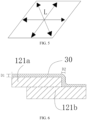
- FIG. 3 is an electron microscope picture of the first texture structure 12 on the rear surface of the semiconductor substrate of the solar cell according to an embodiment of the present disclosure.
- the first texture structure 12 includes two or more first substructures 121 at least partially stacked on one another.
- the first texture structure 12 presents a non-pyramid-shaped microstructure profile.
- the first texture structure may present a substantially "step" profile, and the first substructure 121 may be regarded as a stair of the "step”.
- FIG. 4a is a schematic diagram of three layers of first substructures partially stacked
- FIG. 4b is a schematic diagram of two layers of first substructures partially stacked.
- Reference sign 121a denotes the outermost first substructure in the first texture structure away from the rear surface
- 121b denotes an adjacent first substructure.
- a distance H between a top surface of the outermost first substructure 121a and a top surface of the first substructure 121b adjacent thereto is less than or equal to 2 ⁇ m, which may be 2 ⁇ m, 1.8 ⁇ m, 1.5 ⁇ m, 1.2 ⁇ m, 1.1 ⁇ m, 1.0 ⁇ m, 0.8 ⁇ m, 0.5 ⁇ m, 0.3 ⁇ m, 0.2 ⁇ m, 0.1 ⁇ m or the like.
- the distance H is more than 2 ⁇ m
- the roughness of the first texture structure is excessively large, and the thickness of the tunnel oxide layer 30 formed on the first texture structure is larger, which bring adverse effects to the formation of the tunnel oxide layer with high density and high uniformity, thereby affecting tunneling and passivation effects of the tunnel oxide layer 30.
- the thickness of the tunnel oxide layer formed on the first texture structure is smaller, which brings adverse effects to the contact with an electrode paste.
- the distance between the top surface of the outermost first substructure 121a and the top surface of the first substructure 121b adjacent thereto ranges from 0.3 ⁇ m to 1.2 ⁇ m.
- a distance H between a top surface of the first substructure 121a in any layer and a top surface of the first substructure 121b in an adjacent layer is less than or equal to 2 ⁇ m.
- the distance between the top surface of the outermost first substructure 121a and the top surface of the first substructure 121b adjacent thereto is controlled to be less than or equal to 2 ⁇ m, so that the roughness of the first texture structure is controlled within a desired range, which helps to improve the uniformity of the tunnel oxide layer formed on the first texture structure, ensure better performance of the tunnel oxide layer formed, further inhibit a high local phosphorus concentration caused by phosphorous diffusion, reduce contact resistivity, improve the open-circuit voltage of the solar cell, and improve the fill factor and photoelectric conversion efficiency.
- a one-dimensional size L of the top surface of the outermost first substructure 121a is less than or equal to 45 ⁇ m, that is, 0 ⁇ L ⁇ 45 ⁇ m. In an embodiment, the one-dimensional size L is within a range of 2 ⁇ m to 45 ⁇ m.
- the one-dimensional size L of the top surface may be a length, width, diagonal length or circular diameter of the surface, which is not limited herein.
- the one-dimensional size may be an average value of one-dimensional sizes of top surfaces of a plurality of outermost first substructures within a preset range region of the rear surface of the substrate.
- An average one-dimensional size of the top surface of the outermost first substructure may be 2 ⁇ m, 5 ⁇ m, 8 ⁇ m, 12 ⁇ m, 15 ⁇ m, 18 ⁇ m, 20 ⁇ m, 25 ⁇ m, 28 ⁇ m, 30 ⁇ m, 35 ⁇ m, 40 ⁇ m, 42 ⁇ m, 40 ⁇ m, 45 ⁇ m or the like.
- an average one-dimensional size of the top surface of the outermost first substructure ranges from 10 ⁇ m to 15 ⁇ m.
- the first texture structure further includes two or more adjacent second substructures 122 that are not stacked, and a one-dimensional size L of a top surface of the second substructure 122 away from the rear surface is less than or equal to 45 ⁇ m, that is, 0 ⁇ L ⁇ 45 ⁇ m.
- the one-dimensional size L of the second substructure 122 is within a range of 2 ⁇ m to 45 ⁇ m, which may be 2 ⁇ m, 5 ⁇ m, 8 ⁇ m, 12 ⁇ m, 15 ⁇ m, 18 ⁇ m, 20 ⁇ m, 25 ⁇ m, 28 ⁇ m, 30 ⁇ m, 32 ⁇ m, 35 ⁇ m, 45 ⁇ m or the like.
- the top surface of the first substructure and/or the top surface of the second substructure of the rear surface is a polygonal plane.
- the polygonal plane is in a shape of at least one of a diamond, a square, a trapezoid, a substantially diamond, a substantially square and a substantially trapezoid. It shall be understood that, during actual manufacturing process, the top surface of the first substructure or second substructure presents a profile of an irregular polygon plane, and wholly presents a profile of a substantially diamond, a square and a trapezoid.
- the manufacturing of subsequent passivation film layers may damage original structures of the second texture structure and the first texture structure to some extent.
- the second texture structure may also include a small number of non-pyramid-shaped microstructures formed due to the damages to the spires of the pyramid-shaped microstructures.
- a texture size representing the second texture structure or the first texture structure of the solar cell is measured, such as the one-dimensional size of the top surface of the first substructure and the distance between the surfaces of adjacent first substructures
- surfaces of the film layers are directly measured for calibration through a test instrument (an optical microscope, an atomic force microscope, a scanning electron microscope, a transmission electron microscope, or the like).
- a test instrument an optical microscope, an atomic force microscope, a scanning electron microscope, a transmission electron microscope, or the like.
- the thickness of the film layer is in nanoscale, it can be obtained directly using film layer measurement data corresponding to the second texture structure or the first texture structure, and the film layer measurement data is a sum of the thickness of the film layer and a texture size.
- it can also be obtained by subtracting film layer thickness data from the film layer measurement data.
- the above measurement means are only examples and are not limited in the present disclosure.
- the tunnel oxide layer 30 located on the first texture structure 12 of the rear surface of the semiconductor substrate 10 may have a stacking structure of one or more of a silicon oxide layer, an aluminum oxide layer, a silicon oxynitride layer, a molybdenum oxide layer and a hafnium oxide layer.
- the tunnel oxide layer 30 may also be an oxygen-containing silicon nitride layer, an oxygen-containing silicon carbide layer or the like.
- the tunnel oxide layer 30 has a thickness ranging from 0.8 nm to 2 nm.
- the thickness of the tunnel oxide layer 30 is 0.8 nm, 0.9 nm, 1.0 nm, 1.2 nm, 1.4 nm, 1.6 nm, 1.8 nm, 2 nm or the like.
- the thickness of the tunnel oxide layer 30 refers to a thickness of the tunnel oxide layer relative to a formation surface.
- the thickness of the tunnel oxide layer 30 formed on the first texture structure can be calculated by taking a normal direction of an inclined surface of the substructure as a thickness direction and observing a cross section thereof.
- the thickness of the tunnel oxide layer 30 is excessively large, it may bring adverse effects to reducing the contact resistance of the tunnel oxide layer. A decrease in the fill factor caused by the contact resistance can be inhibited by controlling the thickness of the tunnel oxide layer.
- a band gap width of the tunnel oxide layer 30 is greater than 3.0 eV, and it is generally difficult to transport carriers through the tunnel oxide layer 30 by thermal emission.
- the tunnel oxide layer 30 is very thin and carriers can pass through the tunnel oxide layer 30 through a tunnel effect, so the tunnel oxide layer having a thickness within a range of 0.8 nm to 2nm does not block the transport of most carriers.
- the tunnel oxide layer gradually increases, the tunnel effect of most carriers is affected, and it is difficult to transport the carriers through the tunnel oxide layer 30, and the photoelectric conversion efficiency of the solar cell may gradually decrease.
- the tunnel oxide layer is excessively small, the tunnel oxide layer cannot perform the passivation effect.
- the tunnel oxide layer 30 is a silicon oxide layer, and the tunnel oxide layer 30 has a thickness ranging from 0.8 nm to 1.5 nm.
- a thickness D1 of the tunnel oxide layer on the top surface of the outermost first substructure is less than a thickness D2 of the tunnel oxide layer on a side surface of the outermost first substructure.
- a thickness difference (D2-D1) between the tunnel oxide layer on the top surface of the outermost first substructure and the tunnel oxide layer on a side surface of the outermost substructure is less than or equal to 0.15 nm.
- the thickness difference may be 0.14 nm, 0.13 nm, 0.12 nm, 0.11 nm, 0.10 nm, 0.09 nm, 0.08 nm, 0.07 nm, 0.06 nm, 0.05 nm, 0.04 nm or the like.
- texture structures with different profiles are arranged on the front and rear surfaces of the semiconductor substrate, a pyramidal texture structure is formed on the front surface, and a non-pyramidal texture structure is formed on the rear surface, so that the solar cell formed has a light trap structure at different levels, which increases an effective contact area of light.
- the distance between the top surface of the outermost first substructure and the top surface of the first substructure adjacent thereto is controlled within 2 ⁇ m, which helps to reduce a pinhole in the tunnel oxide layer and then improves the density and uniformity of the tunnel oxide layer, further inhibit a high local doping concentration of the doped conductive layer on the surface of the tunnel oxide layer, reduce contact resistivity, improve the open-circuit voltage of the solar cell, and improve the fill factor and photoelectric conversion efficiency.
- the doped conductive layer 40 may be a doped polycrystalline silicon layer, a doped microcrystalline silicon layer or a doped amorphous silicon layer.
- the doped conductive layer 40 and the semiconductor substrate have doping elements of a same conductivity type.
- the doped conductive layer 40 is an N-type doped polycrystalline silicon layer, an N-type doped microcrystalline silicon layer or an N-type doped amorphous silicon layer, and the doping element may be an N-type doping element such as phosphorus.
- the doped conductive layer 40 has a thickness ranging from 60 nm to 200 nm.
- the doped conductive layer 40 may have a refractive index ranging from 3.5 to 4.5.
- the second passivation layer 50 includes at least one of a silicon nitride layer, a silicon oxide layer and a silicon oxynitride layer.
- the second passivation layer 50 has a thickness ranging from 70 nm to 120 nm.
- the second passivation layer 50 is a silicon nitride layer.
- the silicon nitride layer has a low silicon to nitrogen ratio, and the silicon nitride layer has a refractive index ranging from 1.7 to 2.1, which may be 1.7, 1.8, 1.9, 2.0, 2.1 or the like, and may also be other values in the above range, and is not limited herein.
- the refractive index of the silicon nitride layer is controlled to enable the silicon nitride layer to have low silicon to nitrogen ratio, so that contact resistivity can be reduced during metallization of the second passivation layer 50 formed, so as to further reduce the contact resistivity of the solar cell.
- the silicon nitride layer is located on a surface of the doped conductive layer, and the silicon oxide layer or the silicon oxynitride layer is located on a surface of the silicon nitride layer.
- the solar cell further includes a first electrode 60 and a second electrode 70.
- the first electrode 60 passes through the first passivation layer 20 to form ohmic contact with the P-type doped layer (for example, the boron-doped diffusion layer) on the front surface of the semiconductor substrate 10.
- the second electrode 70 passes through the second passivation layer 50 to form ohmic contact with the doped conductive layer 40.
- the doped conductive layer 40 and the tunnel oxide layer 30 form a passivated contact structure.
- the first electrode 60 and the second electrode 70 may be formed by sintering a metal conductive paste coated on surfaces of the first passivation layer and the second passivation layer.
- the first electrode 60 or the second electrode 70 is made of a metal material such as silver, aluminum, copper or nickel.
- the solar cell formed as shown in FIG. 1 that is, the second texture structure of the pyramid-shaped microstructure formed on the front surface of the semiconductor substrate 10, the first texture structure of the non-pyramid-shaped microstructure formed on the rear surface of the semiconductor substrate, the first passivation layer 20 (for example, a stacked passivation structure of an aluminum oxide layer and a silicon nitride layer) formed on the second texture structure, and the tunnel oxide layer 30, the doped conductive layer 40 and the second passivation layer 50 (for example, a silicon nitride layer) matching one another formed on the first texture structure.
- the solar cell structure formed as above has higher photoelectric conversion efficiency.
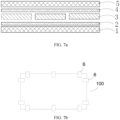
- an embodiment of the present disclosure provides a photovoltaic module including a plurality of solar cell strings.
- the photovoltaic module includes a first cover plate 1, a first packaging adhesive layer 2, a solar cell string 3, a second packaging layer 4 and a second cover plate 5.
- the solar cell string 3 includes a plurality of solar cells (the solar cell as shown in FIG. 1 ) that are connected through a conductive band (not shown).
- the solar cells may be connected by partial stacking or by splicing.
- the first cover plate 1 and the second cover plate 5 are transparent or opaque cover plates, such as glass cover plates or plastic cover plates.
- the first packaging adhesive layer 2 and the second packaging layer 4 may be ethylene-vinyl acetate copolymer (EVA) film, a polyolefin elastomer (POE) film or a polyethylene terephthalate (PET) film, respectively.
- EVA ethylene-vinyl acetate copolymer
- POE polyolefin elastomer
- PET polyethylene terephthalate
- Side edges of the photovoltaic module may also be completely packaged, that is, the side edges of the photovoltaic module are fully packaged with a packaging adhesive tape to prevent a stacking deviation during the stacking of the photovoltaic module.
- the photovoltaic module (the photovoltaic module 100 shown in FIG. 7b ) further includes an edge sealing member 6 fixedly packaged to a partial edge of the photovoltaic module.
- the edge sealing member 6 is fixedly packaged to an edge of the photovoltaic module near a corner.
- the edge sealing member 6 may be a high-temperature resistant tape.
- the high-temperature resistant tape has excellent high-temperature resistance and may not decompose or fall off during the stacking, which can ensure the reliable packaging of the photovoltaic module.
- Two ends of the high-temperature resistant tape are fixed to the second cover plate 5 and the first cover plate 1, respectively.
- the two ends of the high-temperature resistant tape may be bonded to the second cover 5 and the first cover 1, respectively, and the middle thereof can limit a side edge of the photovoltaic module to prevent a stacking deviation of the photovoltaic module during the stacking.
- the present disclosure further provides a method for manufacturing a solar cell for manufacturing the solar cell described above. As shown in FIG. 8 , the method includes the following steps.
- a semiconductor substrate is textured, and a second texture structure is formed on a front surface of the semiconductor substrate, the second texture structure includes a pyramid-shaped microstructure.
- the front surface of the textured semiconductor substrate is doped to form a doped layer.
- a rear surface of the semiconductor substrate is polished with an alkali solution, so that a first texture structure is formed on the rear surface of the semiconductor substrate, the first texture structure includes two or more first substructures at least partially stacked, for the two or more first substructures at least partially stacked, in a direction away from the rear surface and perpendicular to the rear surface, a distance between a top surface of the outermost first substructure and a top surface of the first substructure adjacent thereto is less than or equal to 2 ⁇ m, and a one-dimensional size of the top surface of the outermost first substructure is less than or equal to 45 ⁇ m.
- a tunnel oxide layer is formed on the first texture structure of the rear surface of the semiconductor substrate.
- a polycrystalline silicon layer is formed on a surface of the tunnel oxide layer, and the polycrystalline silicon layer is doped to form a doped conductive layer, the doped conductive layer and the semiconductor substrate having doping elements of a same conductivity type.
- a first passivation layer is formed on the front surface of the semiconductor substrate.
- a second passivation layer is formed on a surface of the doped conductive layer.
- the rear surface of the semiconductor substrate is polished with an alkali solution, so that texture structures with different profiles are formed on the front and rear surfaces of the semiconductor substrate.
- a pyramidal texture structure is formed on the front surface, and a non-pyramidal texture structure is formed on the rear surface, so that the solar cell formed has a light trap structure at different levels, which increases an effective contact area of light.
- the distance between the top surface of the outermost first substructure and the top surface of the first substructure adjacent thereto is controlled within 2 ⁇ m, which helps to reduce a pinhole in the tunnel oxide layer and then improve the density and uniformity of the tunnel oxide layer, further inhibit a high local doping concentration of the doped conductive layer on the surface of the tunnel oxide layer, reduce contact resistivity, improve the open-circuit voltage of the solar cell, and improve the fill factor and photoelectric conversion efficiency.
- a semiconductor substrate is textured, and a second texture structure is formed on a front surface of the semiconductor substrate, the second texture structure includes a pyramid-shaped microstructure.
- the semiconductor substrate may be a crystalline silicon substrate, which is, for example, one of a polycrystalline silicon substrate, a monocrystalline silicon substrate, a microcrystalline silicon substrate and a silicon carbide substrate.
- a specific type of the semiconductor substrate is not limited in the embodiments of the present disclosure.
- the semiconductor substrate is an N-type crystalline silicon substrate (or silicon wafer).
- the semiconductor substrate has a thickness ranging from 60 ⁇ m to 240 ⁇ m, which may be 60 ⁇ m, 80 ⁇ m, 90 ⁇ m, 100 ⁇ m, 120 ⁇ m, 150 ⁇ m, 200 ⁇ m, 240 ⁇ m or the like.
- the doping elements of the semiconductor substrate may be phosphorus, nitrogen and the like.
- an N-type substrate may be textured using, but not limited to, a wet texturing process.
- the texturing may be performed using an alkaline solution such as a potassium hydroxide solution. Since the corrosion of the NaOH solution is anisotropic, a pyramid-shaped microstructure can be manufactured.
- the front surface of the semiconductor substrate 10 has a second texture structure 11, and the second texture structure 11 includes a pyramid-shaped microstructure 111.
- the pyramid-shaped microstructure 111 may have a structure of a tetrahedron, a substantially tetrahedron, a pentahedron, a substantially pentahedron, or the like.
- the pyramid-shaped microstructure 111 may be formed by texturing the semiconductor substrate. The texturing may be chemical etching, laser etching, a mechanical process, plasma etching, or the like.
- the pyramid-shaped microstructure enables a metal paste to better fill the microstructure when the metal paste forms an electrode by screen printing, to obtain better electrode contact, which can effectively reduce series resistance of the solar cell, and improve the fill factor.
- the front surface of the textured semiconductor substrate is doped to form a doped layer.
- a P-type doped layer may be formed on the front surface of the semiconductor substrate by one or more of the processes of high temperature diffusion, slurry doping, and ion implantation, so as to form a PN junction in the semiconductor substrate 10.
- the P-type doped layer is a boron-doped diffusion layer.
- the boron-doped diffusion layer is a P-type doped layer (i.e., P+ layer) formed by using a boron source to diffuse boron atoms to a certain depth on the front surface through a diffusion process.
- the boron source may be liquid boron tribromide.
- a microcrystalline silicon phase of the substrate after boron diffusion treatment is transformed into a polycrystalline silicon phase. Since the surface of the semiconductor substrate has a high concentration of boron, a borosilicate glass (BSG) layer is generally formed.
- BSG borosilicate glass
- the method further includes: removing the borosilicate glass layer from the rear surface of the semiconductor substrate with a prepared mixed acid, the mixed acid includes hydrogen fluoride having a mass fraction of 0.1% to 10%, sulfuric acid having a mass fraction of 10% to 20% and nitric acid having a mass fraction of 25% to 50%; and washing and drying the rear surface of the semiconductor substrate after pickling.
- the rear surface of the semiconductor substrate is coated to form part of the borosilicate glass, which shall be removed. It shall be noted that a porous structure may appear on the rear surface of the semiconductor substrate after pickling.
- a pickling time ranges from 10 seconds to 180 seconds
- a pickling temperature ranges from 7°C to 20°C, that is, the borosilicate glass on the rear surface of the semiconductor substrate is removed by pickling at room temperature to expose a body of the semiconductor substrate.
- the rear surface of the semiconductor substrate is polished with the alkali solution, so that a first texture structure is formed on the rear surface of the semiconductor substrate.
- the rear surface of the semiconductor substrate is cleaned with the alkali solution having a mass fraction of 5% to 15% to remove porous silicon.
- Micro-liquid droplets of the alkali solution are dropped by spraying to the rear surface of the semiconductor substrate for roughening treatment, and then pre-cleaning is performed with a hydrofluoric acid having a mass fraction of 5% to 10%.
- the rear surface of the semiconductor substrate is polished with a polishing liquid at a polishing temperature ranging from 70°C to 80°C for a polishing time less than 260 seconds.
- the polishing liquid includes NaOH having a mass fraction of 1% to 15%, KOH having a mass fraction of 1% to 15% and an additive having a mass fraction of 0.5% to 2.5%.
- the polishing liquid may be designated as the etching solution.
- Organic components in the etching solution are removed by a mixture of potassium hydroxide having a mass fraction of 5% to 15% and hydrogen peroxide having a mass fraction of 15% to 40%.
- the polished semiconductor substrate is washed and dried.
- the borosilicate glass layer on the front surface of the semiconductor substrate shall be protected, for example, by a mask.
- the alkali solutions contain organic bases and/or inorganic bases.
- the inorganic bases may be NaOH, KOH, Ga(OH) 2 , NH 3 .H 2 O, and the organic bases may be triethylamine, nitrophenol, pyridine, quinine, colchicine, and the like.
- the additive in the polishing liquid may be a buffer solution composed of sodium sulfonate, maleic anhydride, alkyl glycoside, and the like.
- the polishing temperature may be 70°C, 72°C, 74°C, 75°C, 78°C, 79°C, 80°C or the like, and the polishing time may be 250 seconds, 240 seconds, 230 seconds, 220 seconds, 200 seconds, 180 seconds, 160 seconds, 140 seconds, 120 seconds, 100 seconds, 80 seconds or the like, which may also be other values in the above ranges.
- a polishing weight loss of the semiconductor substrate is less than 0.3 g.
- a shape of the substructure in the first texture structure after polishing may be adjusted by controlling the polishing time and the polishing temperature, so that in the two or more first substructures at least partially stacked a distance between a top surface of the outermost first substructure and a top surface of the first substructure adjacent thereto is less than or equal to 2 ⁇ m in a direction away from the rear surface and perpendicular to the rear surface, so as to increase the roughness of the rear surface of the semiconductor substrate.
- the first texture structure including a non-pyramid-shaped microstructure may be formed by hot-air drying the surface of the semiconductor substrate.
- FIG. 3 is an electron microscope picture of the first texture structure 12 on the rear surface of the semiconductor substrate of the solar cell according to an embodiment of the present disclosure.
- the first texture structure 12 includes two or more first substructures 121 at least partially stacked.
- FIG. 4a is a schematic diagram of three layers of first substructures partially stacked
- FIG. 4b is a schematic diagram of two layers of first substructures partially stacked.
- Reference sign 121a denotes the outermost first substructure in the first texture structure away from the rear surface
- 121b denotes the innermost first substructure in the first texture structure close to the rear surface.
- a distance H between a top surface of the outermost first substructure 121a and a top surface of the first substructure 121b adjacent thereto is less than or equal to 2 ⁇ m, which may be 2 ⁇ m, 1.8 ⁇ m, 1.5 ⁇ m, 1.2 ⁇ m, 1.1 ⁇ m, 1.0 ⁇ m, 0.8 ⁇ m, 0.5 ⁇ m, 0.3 ⁇ m, 0.2 ⁇ m, 0.1 ⁇ m or the like.
- the roughness of the first texture structure is excessively large, and the thickness of the tunnel oxide layer 30 formed on the first texture structure is larger, which brings adverse effects to the formation of the tunnel oxide layer with high density and high uniformity, thereby affecting tunneling and passivation effects of the tunnel oxide layer 30. If the roughness of the first texture structure is excessively small, the thickness of the tunnel oxide layer formed on the first texture structure is smaller, which brings adverse effects to the contact with an electrode paste.
- the distance between the top surface of the outermost first substructure 121a and the top surface of the first substructure 121b adjacent thereto ranges from 0.3 ⁇ m to 1.2 ⁇ m.
- a distance H between a top surface of the first substructure 121a in any layer and a top surface of the first substructure 121b in an adjacent layer is less than or equal to 2 ⁇ m.
- the distance between the top surface of the outermost first substructure 121a and the top surface of the first substructure 121b adjacent thereto is controlled to be less than or equal to 2 ⁇ m, so that the roughness of the first texture structure is controlled within a desired range, which helps to improve the uniformity of the tunnel oxide layer formed on the first texture structure, ensure better performance of the tunnel oxide layer formed, further inhibit a high local phosphorus concentration caused by phosphorous diffusion, reduce contact resistivity, improve the open-circuit voltage of the solar cell, and improve the fill factor and photoelectric conversion efficiency.
- a one-dimensional size L of the top surface of the outermost first substructure 121a is less than or equal to 45 ⁇ m. In an embodiment, the one-dimensional size L is within a range of 2 ⁇ m to 45 ⁇ m.
- the one-dimensional size L of the top surface may be a length, width, diagonal length or circular diameter of the surface, which is not limited herein.
- the one-dimensional size may be an average value of one-dimensional sizes of top surfaces of a plurality of outermost first substructures within a preset range region of the rear surface of the substrate.
- An average one-dimensional size of the top surface of the outermost first substructure may be 2 ⁇ m, 5 ⁇ m, 8 ⁇ m, 12 ⁇ m, 15 ⁇ m, 18 ⁇ m, 20 ⁇ m, 25 ⁇ m, 28 ⁇ m, 30 ⁇ m, 35 ⁇ m, 40 ⁇ m, 42 ⁇ m, 40 ⁇ m, 45 ⁇ m or the like.
- an average one-dimensional size of the top surface of the outermost first substructure ranges from 10 ⁇ m to 15 ⁇ m.
- the first texture structure further includes two or more adjacent second substructures 122 not stacked, and a one-dimensional size L of a top surface of the second substructure 122 away from the rear surface is less than or equal to 45 ⁇ m.
- the one-dimensional size L of the first substructure 122 is within a range of 2 ⁇ m to 45 ⁇ m, which may be 2 ⁇ m, 5 ⁇ m, 8 ⁇ m, 12 ⁇ m, 15 ⁇ m, 18 ⁇ m, 20 ⁇ m, 25 ⁇ m, 28 ⁇ m, 30 ⁇ m, 32 ⁇ m, 35 ⁇ m, 45 ⁇ m or the like.
- the top surface of the first substructure and/or the top surface of the second substructure of the rear surface is a polygonal plane.
- the polygonal plane is in a shape of at least one of a diamond, a square, a trapezoid, a substantially diamond, a substantially square and a substantially trapezoid. It shall be understood that, during actual manufacturing, the top surface of the first substructure or second substructure presents a profile of an irregular polygon plane, and presents in entirety a profile of a substantially diamond, a square and a trapezoid.
- a tunnel oxide layer is formed on the first texture structure of the rear surface of the semiconductor substrate.
- the rear surface of the semiconductor substrate may be etched and then treated by ozone oxidation, high temperature thermal oxidation, nitric acid oxidation, chemical vapor deposition and low-pressure chemical vapor deposition to form the tunnel oxide layer 30.
- the tunnel oxide layer 30 is deposited on the rear surface of the semiconductor substrate by a temperature change process and chemical vapor deposition. During the deposition, a heating rate is controlled to range from 0.5°C/min to 3°C/min, a deposition temperature is controlled to range from 560°C to 620°C and a deposition time is controlled to range from 3 min to 10 min.
- the deposition temperature may be 560°C, 570°C, 580°C, 590°C, 600°C, 610°C, 615°C, 620°C or the like
- the deposition time may be 3 min, 4 min, 5 min, 6 min, 7 min, 8 min, 9 min, 10 min or the like
- the heating rate may be 0.5 °C/min, 0.8 °C/min, 1.0 °C/min, 1.2 °C/min, 1.5 °C/min, 2.0 °C/min, 2.5 °C/min, 3 °C/min or the like, which may also be other values in the above ranges and are not limited herein.
- the tunnel oxide layer 30 is deposited on the rear surface of the semiconductor substrate by low-pressure chemical vapor deposition, which can reduce the influence of a high local doping concentration of the thinner tunnel oxide layer 30 in subsequent high temperature doping treatment and reduce the fluctuation of the open-circuit voltage.
- the tunnel oxide layer 30 formed by the temperature change process and low-pressure chemical vapor deposition can increase the open-circuit voltage of the solar cell by 4 mV to 6 mV.
- the tunnel oxide layer 30 may have a stacking structure of one or more of a silicon oxide layer, an aluminum oxide layer, a silicon oxynitride layer, a molybdenum oxide layer and a hafnium oxide layer. In other embodiments, the tunnel oxide layer 30 may also be an oxygen-containing silicon nitride layer, an oxygen-containing silicon carbide layer or the like.
- the tunnel oxide layer 30 has a thickness ranging from 0.8 nm to 2 nm. For example, the thickness of the tunnel oxide layer 30 is 0.8 nm, 0.9 nm, 1.0 nm, 1.2 nm, 1.4 nm, 1.6 nm, 1.8 nm, 2 nm or the like.
- the thickness of the tunnel oxide layer 30 refers to a thickness of the tunnel oxide layer relative to a formation surface.
- the thickness of the tunnel oxide layer 30 formed on the first texture structure can be calculated by taking a normal direction of an inclined surface of the substructure as a thickness direction and observing a cross section thereof.
- the thickness of the tunnel oxide layer 30 is excessively large, it brings adverse effects to reducing the contact resistance of the tunnel oxide layer. A decrease in the fill factor caused by the contact resistance can be inhibited by controlling the thickness of the tunnel oxide layer.
- a band gap width of the tunnel oxide layer 30 is greater than 3.0 eV, and it is generally difficult to transport carriers through the tunnel oxide layer 30 by thermal emission.
- the tunnel oxide layer 30 is very thin and carriers can pass through the tunnel oxide layer 30 through a tunnel effect, so the tunnel oxide layer having a thickness within a range of 0.8 nm to 2nm does not block the transport of most carriers.
- the tunnel oxide layer gradually increases, the tunnel effect of most carriers is affected, and it is difficult to transport the carriers through the tunnel oxide layer 30, and the photoelectric conversion efficiency of the solar cell may gradually decrease.
- the tunnel oxide layer is excessively small, the tunnel oxide layer cannot have a passivation effect.
- the tunnel oxide layer 30 is a silicon oxide layer, and the tunnel oxide layer 30 has a thickness ranging from 0.8 nm to 1.5 nm.
- a thickness D1 of the tunnel oxide layer on the top surface of the outermost first substructure is less than a thickness D2 of the tunnel oxide layer on a side surface of the outermost first substructure.
- a thickness difference (D2-D1) between the tunnel oxide layer on the top surface of the outermost first substructure and the tunnel oxide layer on a side surface of the outermost substructure is less than or equal to 0.15 nm.
- the thickness difference may be 0.14 nm, 0.13 nm, 0.12 nm, 0.11 nm, 0.10 nm, 0.09 nm, 0.08 nm, 0.07 nm, 0.06 nm, 0.05 nm, 0.04 nm or the like.
- the tunnel oxide layer on the top surface of the outermost first substructure and the tunnel oxide layer on the side surface of the outermost substructure are excessively large, the thickness of the tunnel oxide layer has poor uniformity, a current density of the solar cell may be affected, and the open-circuit voltage of the solar cell decreases.
- a polycrystalline silicon layer is formed on a surface of the tunnel oxide layer, and the polycrystalline silicon layer is doped to form a doped conductive layer, a conductivity type of the doped conductive layer is the same as that of the semiconductor substrate.
- the polycrystalline silicon layer is deposited on the surface of the tunnel oxide layer by any one of physical vapor deposition, chemical vapor deposition, plasma enhanced chemical vapor deposition and atomic layer deposition.
- the chemical vapor deposition may be low-pressure chemical vapor deposition or atmospheric chemical vapor deposition.
- the deposition of the tunnel oxide layer and the polycrystalline silicon layer and the doping of the polycrystalline silicon layer are all performed in a low-pressure chemical vapor deposition device.
- the alkali-polished semiconductor substrate is placed in a deposition device, an oxygen source (e.g. oxygen, nitrous oxide, or ozone) of 20 L to 60 L is introduced, and the deposition device is heated to 560°C to 620°C according to a heating rate ranging from 0.5 °C/min to 3 °C/min for a deposition time ranging from 3 min to 10 min to form the tunnel oxide layer 30.
- an oxygen source e.g. oxygen, nitrous oxide, or ozone
- the polycrystalline silicon layer is doped in situ to form the doped conductive layer 40.
- the doped conductive layer 40 may be a doped polycrystalline silicon layer.
- the doped conductive layer 40 and the semiconductor substrate have doping elements of a same conductivity type.
- a microcrystalline silicon layer or an amorphous silicon layer may also be deposited on the surface of the tunnel oxide layer 30 and doped in situ to form a doped microcrystalline silicon layer or doped amorphous silicon layer, that is, the doped conductive layer 40.
- the doped conductive layer 40 is an N-type doped polycrystalline silicon layer, an N-type doped microcrystalline silicon layer or an N-type doped amorphous silicon layer, and the doping element may be an N-type doping element such as phosphorus.
- the doped conductive layer 40 has a thickness ranging from 60 nm to 200 nm.
- the doped conductive layer 40 has a refractive index ranging from 3.5 to 4.5.
- the method further includes: performing high-temperature annealing treatment and cleaning treatment after the doped polycrystalline silicon layer is deposited in situ.
- Embodiments of the present disclosure does not limit how the high-temperature annealing treatment and the cleaning treatment are performed.
- the high-temperature annealing treatment deals with the deposited polycrystalline silicon layer, which enables the polycrystalline silicon layer to better crystalize.
- An annealing temperature ranges from 700°C to 1000°C.
- PSG phosphorosilicate glass
- the cleaning treatment is intended to remove a phosphorosilicate glass (PSG) layer formed during the phosphorus doping. Due to the high concentration of phosphorus on the surface of the semiconductor substrate, a phosphorosilicate glass (PSG) layer is generally formed during phosphorus diffusion. This phosphorosilicate glass layer has a metal impurity absorption effect, may adversely affect the normal operation of the solar cell, and shall be removed.
- PSG phosphorosilicate glass
- the rear surface of the semiconductor substrate may be placed downward in a chain pickling device (the chain device is at a tape speed of 1.0 /min to 2.0 m/min).
- the semiconductor substrate enters an acid tank to etch away the phosphorosilicate glass (PSG) layer formed on the rear surface by phosphorus diffusion.
- the acid tank is provided with a prepared mixed acid.
- the mixed acid includes hydrogen fluoride with a mass concentration of 2% to 10% and hydrogen chloride with a mass concentration of 2% to 10%.
- a pickling temperature ranges from 15°C to 25°C, and a pickling time ranges from about 30 seconds to 60 seconds.
- the front surface of the semiconductor substrate is covered with a water film, and the borosilicate glass (BSG) layer on the front surface of the semiconductor substrate may also be used as a protective layer.
- BSG borosilicate glass
- a washing process is needed after the pickling.
- a washing time ranges from 10 seconds to 20 seconds, and a washing temperature may range from 15°C to 25°C.
- the semiconductor substrate may also be dried after washing.
- a first passivation layer is formed on the front surface of the semiconductor substrate.
- the first passivation layer 20 may be deposited by plasma enhanced chemical vapor deposition. It is appreciated that, other methods such as organic chemical vapor deposition may also be used. Embodiments of the present disclosure does not limit implementations of the first passivation layer 20.
- the first passivation layer 20 may have, but is not limited to, a monolayer or laminated structure of a silicon nitride layer, a silicon oxynitride layer, a silicon oxide layer and the like. It is appreciated that, the first passivation layer may also be other types of passivation layers. The present disclosure does not limit a specific material of the first passivation layer. For example, in other embodiments, the first passivation layer may also have a stacked structure of silicon dioxide and silicon nitride. The first passivation layer can have a good passivation effect on the semiconductor substrate, which helps to improve the conversion efficiency of the solar cell.
- a second passivation layer is formed on a surface of the doped conductive layer.
- the second passivation layer 50 may be deposited by plasma enhanced chemical vapor deposition. It is appreciated that, other methods such as organic chemical vapor deposition may also be used. Embodiments of the present disclosure does not limit implementations of the second passivation layer 50.
- the second passivation layer 50 includes at least one of a silicon nitride layer, a silicon oxide layer and a silicon oxynitride layer.
- the second passivation layer 50 has a thickness ranging from 70 nm to 120 nm.
- the second passivation layer 50 is a silicon nitride layer.
- the silicon nitride layer has a low silicon to nitrogen ratio, and the silicon nitride layer has a refractive index ranging from 1.7 to 2.1, which may be 1.7, 1.8, 1.9, 2.0, 2.1 or the like, and may also be other values in the above range, which is not limited herein.
- the refractive index of the silicon nitride layer is controlled to enable the silicon nitride layer to possess low silicon to nitrogen ratio, so that contact resistivity can be reduced during metallization of the second passivation layer 50 formed, so as to further reduce the contact resistivity of the solar cell.
- the silicon nitride layer is located on a surface of the doped conductive layer, and the silicon oxide layer or the silicon oxynitride layer is located on a surface of the silicon nitride layer.
- the method further includes: screen-printing and sintering the semiconductor substrate to form an electrode.
- the solar cell further includes a first electrode 60 and a second electrode 70.
- the first electrode 60 passes through the first passivation layer 20 to form ohmic contact with the P-type doped layer (for example, the boron-doped diffusion layer) on the front surface of the semiconductor substrate 10.
- the second electrode 70 passes through the second passivation layer 50 to form ohmic contact with the doped conductive layer 40.
- the doped conductive layer 40 and the tunnel oxide layer 30 form a passivated contact structure.
- the first electrode 60 and the second electrode 70 may be formed by sintering a metal conductive paste coated on surfaces of the first passivation layer and the second passivation layer.
- the first electrode 60 or the second electrode 70 is made of a metal material such as silver, aluminum, copper or nickel.
- Embodiments 1 to 13 and Comparative Examples 1 to 4 of the solar cell manufactured according to the above method are illustrated as below. Parameters are shown in Table 1.
- Table 1 Parameters of the solar cell Sample Second texture structure First texture structure Thickne ss of the tunnel oxide layer (nm) Thickness difference between tunnel oxide layers (nm) First passivation layer Thicknes s of the first passivati on layer (nm) Refractive index of the first passivatio n layer Second passivatio n layer Thickness of the second passivatio n layer (nm) Refractive index of the second passivatio n layer Distance between a top and a bottom of a pyramid-shaped microstructur e ( ⁇ m) Distance between a top surface and a bottom surface of a first substructure ( ⁇ m) One-dimensional size of the top surface of the outermost first substructure ( ⁇ m) Embodiment 1 3.0 1.9 8.6 1.2 0.12 Aluminum oxide + silicon nitride 5+50 1.92 Silicon n
- Table 2 shows parameters used in a deposition process of a tunnel oxide layer and a polycrystalline silicon layer thereon of the solar cell in each embodiment and in each comparative example.
- the silicon substrate is installed in a low-pressure chemical vapor deposition (LPCVD) device, the device is vacuumed and the temperature is raised, oxide gas (e.g., oxygen) having a loading temperature is added, and a three-stage oxidation process is conducted, in which a first oxidation period of 1.2 minutes is performed in the first stage, a second oxidation period of 1.3 minutes is performed in the second stage, and a third oxidation period of 1.5 minutes is performed in the third stage, so as to form the tunnel oxide layer on the silicon substrate.
- LPCVD low-pressure chemical vapor deposition
- the oxide gas is exhausted and nitrogen is added to form an atmosphere in the interior of the device, the temperature of the device is raised to a pre-deposition temperature, a silane gas having a loading temperature is added to the tunnel oxide layer of the silicon substrate for deposition, so as to form the polycrystalline silicon layer.
- a distance between the substructures in the first texture structure of the rear surface of the semiconductor substrate is controlled within an ideal range, which can ensure that the roughness of the rear surface of the semiconductor substrate is within an appropriate range, helps to improve the uniformity of the tunnel oxide layer formed on the first texture structure, ensure better performance of the tunnel oxide layer formed, further inhibit a high local doping concentration of the doped conductive layer, reduce contact resistivity, improve the open-circuit voltage of the solar cell, and improve a fill factor and photoelectric conversion efficiency.
- a distance between a top surface of the outermost first substructure and a top surface of the first substructure adjacent thereto is less than or equal to 2 ⁇ m.
- the uniformity of the tunnel oxide layer decreases, resulting in a high local doping concentration of the doped conductive layer formed on the surface of the tunnel oxide layer.
- the contact resistivity is increased compared with that in Embodiment 1, which leads to the reduction of the open-circuit voltage of the solar cell, as well as the reduction of the fill factor and the photoelectric conversion efficiency.
- the solar cell according to Comparative Example 2 is not subjected to an alkali-polishing process after texturing, the rear surface has a pyramid-shaped microstructure, and the uniformity of the tunnel oxide layer deposited on the pyramid-shaped microstructure decreases, which easily leads to a high local doping concentration of the doped conductive layer formed on the surface of the tunnel oxide layer.
- the contact resistivity is increased compared with that in Embodiment 1, which leads to the reduction of the open-circuit voltage of the solar cell, as well as the reduction of the fill factor and the photoelectric conversion efficiency.
- the solar cell according to Comparative Example 3 through the treatment of the substructure of the first texture structure, inhibits a high local doping concentration of the doped conductive layer, the contact resistivity is difficult to further decrease during the metallization due to the use of a silicon nitride layer with a high silicon to nitrogen ratio.
- the distance between the substructures in the first texture structure of the rear surface of the semiconductor substrate and the refractive index of the second passivation layer are controlled, and a synergistic effect of the two can better reduce the contact resistivity and improve the open-circuit voltage, the fill factor and the photoelectric conversion efficiency of the solar cell.
- the solar cell according to Comparative Example 4 through the treatment of the substructure of the first texture structure, inhibits a high local doping concentration of the doped conductive layer, the contact resistivity increases during the metallization due to the use of an aluminum oxide layer and a silicon nitride layer with a lower overall refractive index as the first passivation layer.
Landscapes
- Photovoltaic Devices (AREA)
- Life Sciences & Earth Sciences (AREA)
- Chemical & Material Sciences (AREA)
- Crystallography & Structural Chemistry (AREA)
- Sustainable Development (AREA)
- Formation Of Insulating Films (AREA)
Applications Claiming Priority (2)
| Application Number | Priority Date | Filing Date | Title |
|---|---|---|---|
| CN202110895225.8A CN115020503B (zh) | 2021-08-04 | 2021-08-04 | 太阳能电池及其制备方法、光伏组件 |
| EP21194044.0A EP4131425B1 (de) | 2021-08-04 | 2021-08-31 | Solarzelle, herstellungsverfahren dafür und photovoltaisches modul |
Related Parent Applications (2)
| Application Number | Title | Priority Date | Filing Date |
|---|---|---|---|
| EP21194044.0A Division EP4131425B1 (de) | 2021-08-04 | 2021-08-31 | Solarzelle, herstellungsverfahren dafür und photovoltaisches modul |
| EP21194044.0A Division-Into EP4131425B1 (de) | 2021-08-04 | 2021-08-31 | Solarzelle, herstellungsverfahren dafür und photovoltaisches modul |
Publications (4)
| Publication Number | Publication Date |
|---|---|
| EP4372829A2 true EP4372829A2 (de) | 2024-05-22 |
| EP4372829A3 EP4372829A3 (de) | 2024-08-07 |
| EP4372829B1 EP4372829B1 (de) | 2025-02-12 |
| EP4372829C0 EP4372829C0 (de) | 2025-02-12 |
Family
ID=77564007
Family Applications (3)
| Application Number | Title | Priority Date | Filing Date |
|---|---|---|---|
| EP21194044.0A Active EP4131425B1 (de) | 2021-08-04 | 2021-08-31 | Solarzelle, herstellungsverfahren dafür und photovoltaisches modul |
| EP24168316.8A Active EP4372829B1 (de) | 2021-08-04 | 2021-08-31 | Solarzelle |
| EP24221281.9A Pending EP4535961A3 (de) | 2021-08-04 | 2021-08-31 | Solarzelle, herstellungsverfahren dafür und fotovoltaisches modul |
Family Applications Before (1)
| Application Number | Title | Priority Date | Filing Date |
|---|---|---|---|
| EP21194044.0A Active EP4131425B1 (de) | 2021-08-04 | 2021-08-31 | Solarzelle, herstellungsverfahren dafür und photovoltaisches modul |
Family Applications After (1)
| Application Number | Title | Priority Date | Filing Date |
|---|---|---|---|
| EP24221281.9A Pending EP4535961A3 (de) | 2021-08-04 | 2021-08-31 | Solarzelle, herstellungsverfahren dafür und fotovoltaisches modul |
Country Status (6)
| Country | Link |
|---|---|
| US (3) | US11581454B1 (de) |
| EP (3) | EP4131425B1 (de) |
| JP (5) | JP7082235B1 (de) |
| CN (2) | CN115020503B (de) |
| AU (7) | AU2021225144B1 (de) |
| DE (2) | DE202021004467U1 (de) |
Cited By (1)
| Publication number | Priority date | Publication date | Assignee | Title |
|---|---|---|---|---|
| US12514021B2 (en) | 2021-08-04 | 2025-12-30 | Shanghai Jinko Green Energy Enterprise Management Co., Ltd. | Solar cell, manufacturing method thereof, and photovoltaic module |
Families Citing this family (19)
| Publication number | Priority date | Publication date | Assignee | Title |
|---|---|---|---|---|
| CN114373831A (zh) * | 2021-12-30 | 2022-04-19 | 通威太阳能(眉山)有限公司 | 一种隧穿氧化层、n型双面太阳能晶硅电池及制备方法 |
| CN116722056A (zh) * | 2022-05-26 | 2023-09-08 | 浙江晶科能源有限公司 | 太阳能电池及太阳能电池的制备方法、光伏组件 |
| CN116722054B (zh) * | 2022-06-10 | 2024-05-10 | 浙江晶科能源有限公司 | 太阳能电池及太阳能电池的制备方法、光伏组件 |
| CN116936658A (zh) | 2022-06-21 | 2023-10-24 | 浙江晶科能源有限公司 | 背接触太阳能电池及光伏组件 |
| CN116130530B (zh) * | 2022-09-07 | 2024-07-05 | 隆基绿能科技股份有限公司 | Topcon太阳能电池及其制备方法 |
| CN117712199A (zh) | 2022-09-08 | 2024-03-15 | 浙江晶科能源有限公司 | 太阳能电池及光伏组件 |
| CN117673176A (zh) | 2022-09-08 | 2024-03-08 | 浙江晶科能源有限公司 | 太阳能电池及光伏组件 |
| CN117238987A (zh) * | 2022-09-08 | 2023-12-15 | 浙江晶科能源有限公司 | 太阳能电池及光伏组件 |
| CN115377252B (zh) * | 2022-10-24 | 2023-01-13 | 英利能源发展(天津)有限公司 | 一种抑制pecvd法生长多晶硅表面爆膜的方法 |
| CN115831789B (zh) * | 2022-11-15 | 2026-04-24 | 浙江晶科能源有限公司 | 一种电池片的制备方法 |
| CN116844937B (zh) * | 2023-06-30 | 2024-04-09 | 淮安捷泰新能源科技有限公司 | 硅片的rca清洗方法 |
| CN117059681B (zh) | 2023-10-09 | 2024-03-29 | 晶科能源(海宁)有限公司 | 太阳能电池及其制造方法、光伏组件 |
| CN118335816A (zh) * | 2023-10-26 | 2024-07-12 | 晶科能源(海宁)有限公司 | 太阳能电池、光伏组件 |
| CN117727809B (zh) | 2024-02-08 | 2024-08-06 | 浙江晶科能源有限公司 | 太阳能电池及光伏组件 |
| CN118658908B (zh) * | 2024-08-20 | 2024-10-22 | 通威太阳能(成都)有限公司 | 一种太阳电池及光伏组件 |
| CN119836011A (zh) * | 2024-09-05 | 2025-04-15 | 隆基绿能科技股份有限公司 | 太阳能电池及制备方法 |
| CN119584717B (zh) * | 2024-12-02 | 2025-06-06 | 隆基绿能科技股份有限公司 | 一种太阳能电池、光伏组件和半导体基片 |
| CN119545972B (zh) * | 2025-01-23 | 2025-04-29 | 鄂尔多斯市隆基光伏科技有限公司 | 一种太阳能电池以及光伏组件 |
| CN119698073A (zh) * | 2025-02-25 | 2025-03-25 | 通威太阳能(成都)有限公司 | 太阳能电池及其制备方法和光伏组件 |
Family Cites Families (42)
| Publication number | Priority date | Publication date | Assignee | Title |
|---|---|---|---|---|
| US5356488A (en) | 1991-12-27 | 1994-10-18 | Rudolf Hezel | Solar cell and method for its manufacture |
| JP2004273829A (ja) * | 2003-03-10 | 2004-09-30 | Sharp Corp | 光電変換装置及びその製造方法 |
| KR20100013649A (ko) | 2008-07-31 | 2010-02-10 | 삼성전자주식회사 | 광전소자 및 이의 제조 방법 |
| NL2003390C2 (en) | 2009-08-25 | 2011-02-28 | Stichting Energie | Solar cell and method for manufacturing such a solar cell. |
| JP2011129867A (ja) * | 2009-11-17 | 2011-06-30 | Shirakuseru Kk | ボロン拡散層を有するシリコン太陽電池セル及びその製造方法 |
| JP5297543B2 (ja) | 2011-03-30 | 2013-09-25 | パナソニック株式会社 | テクスチャ形成面を有するシリコン基板、およびその製造方法 |
| JP5948685B2 (ja) | 2011-12-27 | 2016-07-06 | パナソニックIpマネジメント株式会社 | 太陽電池及びその製造方法 |
| KR101325012B1 (ko) * | 2012-03-21 | 2013-11-04 | 삼성코닝정밀소재 주식회사 | 광전지 모듈용 커버기판 및 이를 구비한 광전지 모듈 |
| US9054255B2 (en) * | 2012-03-23 | 2015-06-09 | Sunpower Corporation | Solar cell having an emitter region with wide bandgap semiconductor material |
| KR101831405B1 (ko) | 2012-03-28 | 2018-02-22 | 엘지전자 주식회사 | 태양 전지 |
| CN102683439A (zh) * | 2012-05-04 | 2012-09-19 | 友达光电股份有限公司 | 光学抗反射结构、其制法以及包含其的太阳能电池 |
| CN104350607B (zh) * | 2012-06-13 | 2018-01-12 | 三菱电机株式会社 | 太阳能电池及其制造方法 |
| CN102856328B (zh) * | 2012-10-10 | 2015-06-10 | 友达光电股份有限公司 | 太阳能电池及其制作方法 |
| US8785233B2 (en) * | 2012-12-19 | 2014-07-22 | Sunpower Corporation | Solar cell emitter region fabrication using silicon nano-particles |
| US20150162487A1 (en) * | 2013-09-16 | 2015-06-11 | Solexel, Inc. | Aluminum oxide passivation for solar cells |
| US9891100B2 (en) * | 2013-10-10 | 2018-02-13 | Apple, Inc. | Electronic device having light sensor package with diffuser for reduced light sensor directionality |
| WO2015122257A1 (ja) | 2014-02-13 | 2015-08-20 | シャープ株式会社 | 光電変換素子 |
| WO2016114271A1 (ja) | 2015-01-14 | 2016-07-21 | シャープ株式会社 | 光電変換素子、それを備えた太陽電池モジュールおよび太陽光発電システム |
| TW201628208A (zh) * | 2015-01-30 | 2016-08-01 | Kingwave Corp | 具表面階層式抗反射層之太陽能電池 |
| JP6613252B2 (ja) * | 2015-02-09 | 2019-11-27 | シャープ株式会社 | 光電変換素子 |
| KR102600379B1 (ko) * | 2015-12-21 | 2023-11-10 | 상라오 징코 솔라 테크놀러지 디벨롭먼트 컴퍼니, 리미티드 | 태양 전지와 그 제조 방법 |
| CN105826405A (zh) * | 2016-05-17 | 2016-08-03 | 常州天合光能有限公司 | 一种单晶硅双面太阳电池及其制备方法 |
| CN105826411B (zh) * | 2016-05-17 | 2017-12-08 | 常州天合光能有限公司 | 单晶硅双面太阳电池及其制备方法 |
| US20180018295A1 (en) | 2016-07-18 | 2018-01-18 | I/O Interconnect, Ltd. | Method for automatically exchanging device-to-host interface direction for usb type-c connections |
| JP7064823B2 (ja) * | 2016-08-31 | 2022-05-11 | 株式会社マテリアル・コンセプト | 太陽電池及びその製造方法 |
| WO2018084159A1 (ja) * | 2016-11-02 | 2018-05-11 | 株式会社カネカ | 太陽電池およびその製造方法、ならびに太陽電池モジュール |
| KR101942783B1 (ko) * | 2016-11-23 | 2019-04-17 | 엘지전자 주식회사 | 태양 전지 및 이의 제조 방법 |
| KR102600449B1 (ko) | 2016-12-22 | 2023-11-10 | 상라오 징코 솔라 테크놀러지 디벨롭먼트 컴퍼니, 리미티드 | 태양 전지 및 이의 제조 방법 |
| KR20180119969A (ko) | 2017-04-26 | 2018-11-05 | 엘지전자 주식회사 | 태양 전지 및 이의 제조 방법 |
| KR102514785B1 (ko) * | 2017-05-19 | 2023-03-29 | 상라오 징코 솔라 테크놀러지 디벨롭먼트 컴퍼니, 리미티드 | 태양 전지 및 이의 제조 방법 |
| KR20190058017A (ko) * | 2017-11-21 | 2019-05-29 | 국방과학연구소 | 질화물계 반도체 수광소자 및 이의 제조방법 |
| CN109545880A (zh) * | 2019-01-21 | 2019-03-29 | 淮海工学院 | 一种单晶硅基类倒金字塔绒面结构背钝化太阳电池及其制备方法 |
| CN110931596A (zh) | 2019-10-31 | 2020-03-27 | 泰州中来光电科技有限公司 | 一种基于pvd技术制备钝化接触结构的方法 |
| CN111180538A (zh) * | 2019-12-31 | 2020-05-19 | 中威新能源(成都)有限公司 | 一种具有金字塔叠加结构的单晶硅片及制备方法 |
| CN111628049A (zh) | 2020-06-11 | 2020-09-04 | 常州时创能源股份有限公司 | 实现空穴局部钝化接触的方法、晶体硅太阳能电池及其制备方法 |
| CN111668345A (zh) * | 2020-06-29 | 2020-09-15 | 浙江晶科能源有限公司 | 一种太阳能电池及其制备方法 |
| CN111739984A (zh) * | 2020-08-10 | 2020-10-02 | 浙江晶科能源有限公司 | 太阳能电池及其制作方法 |
| CN112111279A (zh) * | 2020-08-13 | 2020-12-22 | 天津爱旭太阳能科技有限公司 | 一种太阳能电池制备碱抛光用添加剂及抛光工艺 |
| CN112309849B (zh) * | 2020-09-30 | 2022-11-22 | 英利能源(中国)有限公司 | 一种硅片单面刻蚀抛光的方法 |
| CN212750903U (zh) | 2020-10-15 | 2021-03-19 | 嘉兴阿特斯光伏技术有限公司 | 太阳能电池 |
| CN112466962B (zh) * | 2020-11-19 | 2021-11-23 | 晶科绿能(上海)管理有限公司 | 太阳能电池 |
| CN112599615B (zh) | 2021-03-05 | 2021-08-06 | 浙江正泰太阳能科技有限公司 | 一种具有双面铝浆电极的N型Topcon电池及其制备方法 |
-
2021
- 2021-08-04 CN CN202110895225.8A patent/CN115020503B/zh active Active
- 2021-08-04 CN CN202211229358.2A patent/CN115528121B/zh active Active
- 2021-08-25 JP JP2021137285A patent/JP7082235B1/ja active Active
- 2021-08-27 US US17/459,689 patent/US11581454B1/en active Active
- 2021-08-30 AU AU2021225144A patent/AU2021225144B1/en active Active
- 2021-08-31 EP EP21194044.0A patent/EP4131425B1/de active Active
- 2021-08-31 DE DE202021004467.1U patent/DE202021004467U1/de active Active
- 2021-08-31 DE DE202021004469.8U patent/DE202021004469U1/de active Active
- 2021-08-31 EP EP24168316.8A patent/EP4372829B1/de active Active
- 2021-08-31 EP EP24221281.9A patent/EP4535961A3/de active Pending
-
2022
- 2022-05-24 JP JP2022084397A patent/JP7174188B1/ja active Active
- 2022-07-22 AU AU2022206802A patent/AU2022206802B2/en active Active
- 2022-10-12 US US17/964,190 patent/US11824136B2/en active Active
- 2022-11-02 JP JP2022176074A patent/JP7331232B2/ja active Active
- 2022-12-09 AU AU2022283784A patent/AU2022283784C1/en active Active
-
2023
- 2023-04-10 US US18/132,796 patent/US11929449B2/en active Active
- 2023-08-09 JP JP2023129723A patent/JP7612780B2/ja active Active
- 2023-12-05 AU AU2023278001A patent/AU2023278001B2/en active Active
-
2024
- 2024-11-15 AU AU2024264689A patent/AU2024264689B2/en active Active
- 2024-12-25 JP JP2024228550A patent/JP2025041865A/ja active Pending
- 2024-12-30 AU AU2024287247A patent/AU2024287247A1/en not_active Withdrawn
-
2025
- 2025-12-23 AU AU2025287271A patent/AU2025287271A1/en active Pending
Cited By (1)
| Publication number | Priority date | Publication date | Assignee | Title |
|---|---|---|---|---|
| US12514021B2 (en) | 2021-08-04 | 2025-12-30 | Shanghai Jinko Green Energy Enterprise Management Co., Ltd. | Solar cell, manufacturing method thereof, and photovoltaic module |
Also Published As
Similar Documents
| Publication | Publication Date | Title |
|---|---|---|
| EP4131425B1 (de) | Solarzelle, herstellungsverfahren dafür und photovoltaisches modul | |
| EP4148808A1 (de) | Solarzelle, verfahren zur herstellung der solarzelle und fotovoltaisches modul | |
| US12132138B2 (en) | Solar cell, manufacturing method thereof, and photovoltaic module |
Legal Events
| Date | Code | Title | Description |
|---|---|---|---|
| PUAI | Public reference made under article 153(3) epc to a published international application that has entered the european phase |
Free format text: ORIGINAL CODE: 0009012 |
|
| STAA | Information on the status of an ep patent application or granted ep patent |
Free format text: STATUS: REQUEST FOR EXAMINATION WAS MADE |
|
| 17P | Request for examination filed |
Effective date: 20240403 |
|
| AC | Divisional application: reference to earlier application |
Ref document number: 4131425 Country of ref document: EP Kind code of ref document: P |
|
| AK | Designated contracting states |
Kind code of ref document: A2 Designated state(s): AL AT BE BG CH CY CZ DE DK EE ES FI FR GB GR HR HU IE IS IT LI LT LU LV MC MK MT NL NO PL PT RO RS SE SI SK SM TR |
|
| REG | Reference to a national code |
Ref country code: DE Free format text: PREVIOUS MAIN CLASS: H01L0031068000 Ipc: H01L0031023600 Ref country code: DE Ref legal event code: R079 Ref document number: 602021026222 Country of ref document: DE Free format text: PREVIOUS MAIN CLASS: H01L0031068000 Ipc: H01L0031023600 |
|
| PUAL | Search report despatched |
Free format text: ORIGINAL CODE: 0009013 |
|
| AK | Designated contracting states |
Kind code of ref document: A3 Designated state(s): AL AT BE BG CH CY CZ DE DK EE ES FI FR GB GR HR HU IE IS IT LI LT LU LV MC MK MT NL NO PL PT RO RS SE SI SK SM TR |
|
| RIC1 | Information provided on ipc code assigned before grant |
Ipc: H01L 31/068 20120101ALI20240701BHEP Ipc: H01L 31/0216 20140101ALI20240701BHEP Ipc: H01L 31/0236 20060101AFI20240701BHEP |
|
| GRAP | Despatch of communication of intention to grant a patent |
Free format text: ORIGINAL CODE: EPIDOSNIGR1 |
|
| STAA | Information on the status of an ep patent application or granted ep patent |
Free format text: STATUS: GRANT OF PATENT IS INTENDED |
|
| GRAS | Grant fee paid |
Free format text: ORIGINAL CODE: EPIDOSNIGR3 |
|
| INTG | Intention to grant announced |
Effective date: 20241205 |
|
| GRAA | (expected) grant |
Free format text: ORIGINAL CODE: 0009210 |
|
| STAA | Information on the status of an ep patent application or granted ep patent |
Free format text: STATUS: THE PATENT HAS BEEN GRANTED |
|
| AC | Divisional application: reference to earlier application |
Ref document number: 4131425 Country of ref document: EP Kind code of ref document: P |
|
| AK | Designated contracting states |
Kind code of ref document: B1 Designated state(s): AL AT BE BG CH CY CZ DE DK EE ES FI FR GB GR HR HU IE IS IT LI LT LU LV MC MK MT NL NO PL PT RO RS SE SI SK SM TR |
|
| REG | Reference to a national code |
Ref country code: GB Ref legal event code: FG4D |
|
| REG | Reference to a national code |
Ref country code: CH Ref legal event code: EP |
|
| REG | Reference to a national code |
Ref country code: DE Ref legal event code: R096 Ref document number: 602021026222 Country of ref document: DE |
|
| REG | Reference to a national code |
Ref country code: IE Ref legal event code: FG4D |
|
| U01 | Request for unitary effect filed |
Effective date: 20250212 |
|
| U07 | Unitary effect registered |
Designated state(s): AT BE BG DE DK EE FI FR IT LT LU LV MT NL PT RO SE SI Effective date: 20250219 |
|
| U1N | Appointed representative for the unitary patent procedure changed after the registration of the unitary effect |
Representative=s name: RGTH; DE |
|
| U30 | Action lodged before the upc [information provided by the upc] |
Free format text: ACTION-TYPE: INFRINGEMENT ACTION; CASE-NUMBER: ACT_7567/2025 Effective date: 20250213 |
|
| PG25 | Lapsed in a contracting state [announced via postgrant information from national office to epo] |
Ref country code: RS Free format text: LAPSE BECAUSE OF FAILURE TO SUBMIT A TRANSLATION OF THE DESCRIPTION OR TO PAY THE FEE WITHIN THE PRESCRIBED TIME-LIMIT Effective date: 20250512 |
|
| PG25 | Lapsed in a contracting state [announced via postgrant information from national office to epo] |
Ref country code: PL Free format text: LAPSE BECAUSE OF FAILURE TO SUBMIT A TRANSLATION OF THE DESCRIPTION OR TO PAY THE FEE WITHIN THE PRESCRIBED TIME-LIMIT Effective date: 20250212 |
|
| PG25 | Lapsed in a contracting state [announced via postgrant information from national office to epo] |
Ref country code: ES Free format text: LAPSE BECAUSE OF FAILURE TO SUBMIT A TRANSLATION OF THE DESCRIPTION OR TO PAY THE FEE WITHIN THE PRESCRIBED TIME-LIMIT Effective date: 20250212 |
|
| PG25 | Lapsed in a contracting state [announced via postgrant information from national office to epo] |
Ref country code: IS Free format text: LAPSE BECAUSE OF FAILURE TO SUBMIT A TRANSLATION OF THE DESCRIPTION OR TO PAY THE FEE WITHIN THE PRESCRIBED TIME-LIMIT Effective date: 20250612 Ref country code: NO Free format text: LAPSE BECAUSE OF FAILURE TO SUBMIT A TRANSLATION OF THE DESCRIPTION OR TO PAY THE FEE WITHIN THE PRESCRIBED TIME-LIMIT Effective date: 20250512 |
|
| PG25 | Lapsed in a contracting state [announced via postgrant information from national office to epo] |
Ref country code: HR Free format text: LAPSE BECAUSE OF FAILURE TO SUBMIT A TRANSLATION OF THE DESCRIPTION OR TO PAY THE FEE WITHIN THE PRESCRIBED TIME-LIMIT Effective date: 20250212 |
|
| PG25 | Lapsed in a contracting state [announced via postgrant information from national office to epo] |
Ref country code: GR Free format text: LAPSE BECAUSE OF FAILURE TO SUBMIT A TRANSLATION OF THE DESCRIPTION OR TO PAY THE FEE WITHIN THE PRESCRIBED TIME-LIMIT Effective date: 20250513 |
|
| U30 | Action lodged before the upc [information provided by the upc] |
Free format text: ACTION-TYPE: COUNTERCLAIMS REVOCATION; CASE-NUMBER: PR_CC_21209/2025 Effective date: 20250721 Free format text: ACTION-TYPE: COUNTERCLAIMS REVOCATION; CASE-NUMBER: CC_21209/2025 Effective date: 20250721 |
|
| U20 | Renewal fee for the european patent with unitary effect paid |
Year of fee payment: 5 Effective date: 20250827 |
|
| PG25 | Lapsed in a contracting state [announced via postgrant information from national office to epo] |
Ref country code: SM Free format text: LAPSE BECAUSE OF FAILURE TO SUBMIT A TRANSLATION OF THE DESCRIPTION OR TO PAY THE FEE WITHIN THE PRESCRIBED TIME-LIMIT Effective date: 20250212 |
|
| PG25 | Lapsed in a contracting state [announced via postgrant information from national office to epo] |
Ref country code: CZ Free format text: LAPSE BECAUSE OF FAILURE TO SUBMIT A TRANSLATION OF THE DESCRIPTION OR TO PAY THE FEE WITHIN THE PRESCRIBED TIME-LIMIT Effective date: 20250212 |
|
| PG25 | Lapsed in a contracting state [announced via postgrant information from national office to epo] |
Ref country code: SK Free format text: LAPSE BECAUSE OF FAILURE TO SUBMIT A TRANSLATION OF THE DESCRIPTION OR TO PAY THE FEE WITHIN THE PRESCRIBED TIME-LIMIT Effective date: 20250212 |
|
| PLBE | No opposition filed within time limit |
Free format text: ORIGINAL CODE: 0009261 |
|
| STAA | Information on the status of an ep patent application or granted ep patent |
Free format text: STATUS: NO OPPOSITION FILED WITHIN TIME LIMIT |
|
| REG | Reference to a national code |
Ref country code: CH Ref legal event code: L10 Free format text: ST27 STATUS EVENT CODE: U-0-0-L10-L00 (AS PROVIDED BY THE NATIONAL OFFICE) Effective date: 20251224 |
|
| 26N | No opposition filed |
Effective date: 20251113 |
|
| REG | Reference to a national code |
Ref country code: CH Ref legal event code: H13 Free format text: ST27 STATUS EVENT CODE: U-0-0-H10-H13 (AS PROVIDED BY THE NATIONAL OFFICE) Effective date: 20260324 |
|
| PG25 | Lapsed in a contracting state [announced via postgrant information from national office to epo] |
Ref country code: MC Free format text: LAPSE BECAUSE OF FAILURE TO SUBMIT A TRANSLATION OF THE DESCRIPTION OR TO PAY THE FEE WITHIN THE PRESCRIBED TIME-LIMIT Effective date: 20250212 |
|
| PG25 | Lapsed in a contracting state [announced via postgrant information from national office to epo] |
Ref country code: CH Free format text: LAPSE BECAUSE OF NON-PAYMENT OF DUE FEES Effective date: 20250831 |