EP4354477B1 - Ferroelektrischer nanopartikelkondensator für nichtbinäre logik - Google Patents
Ferroelektrischer nanopartikelkondensator für nichtbinäre logik Download PDFInfo
- Publication number
- EP4354477B1 EP4354477B1 EP22200942.5A EP22200942A EP4354477B1 EP 4354477 B1 EP4354477 B1 EP 4354477B1 EP 22200942 A EP22200942 A EP 22200942A EP 4354477 B1 EP4354477 B1 EP 4354477B1
- Authority
- EP
- European Patent Office
- Prior art keywords
- ferroelectric
- nanoparticles
- capacitor
- nanoparticle
- charge
- Prior art date
- Legal status (The legal status is an assumption and is not a legal conclusion. Google has not performed a legal analysis and makes no representation as to the accuracy of the status listed.)
- Active
Links
Images



Classifications
-
- H—ELECTRICITY
- H01—ELECTRIC ELEMENTS
- H01G—CAPACITORS; CAPACITORS, RECTIFIERS, DETECTORS, SWITCHING DEVICES, LIGHT-SENSITIVE OR TEMPERATURE-SENSITIVE DEVICES OF THE ELECTROLYTIC TYPE
- H01G7/00—Capacitors in which the capacitance is varied by non-mechanical means; Processes of their manufacture
- H01G7/06—Capacitors in which the capacitance is varied by non-mechanical means; Processes of their manufacture having a dielectric selected for the variation of its permittivity with applied voltage, i.e. ferroelectric capacitors
-
- H—ELECTRICITY
- H01—ELECTRIC ELEMENTS
- H01G—CAPACITORS; CAPACITORS, RECTIFIERS, DETECTORS, SWITCHING DEVICES, LIGHT-SENSITIVE OR TEMPERATURE-SENSITIVE DEVICES OF THE ELECTROLYTIC TYPE
- H01G4/00—Fixed capacitors; Processes of their manufacture
- H01G4/40—Structural combinations of fixed capacitors with other electric elements, the structure mainly consisting of a capacitor, e.g. RC combinations
-
- G—PHYSICS
- G06—COMPUTING OR CALCULATING; COUNTING
- G06N—COMPUTING ARRANGEMENTS BASED ON SPECIFIC COMPUTATIONAL MODELS
- G06N3/00—Computing arrangements based on biological models
- G06N3/02—Neural networks
- G06N3/04—Architecture, e.g. interconnection topology
-
- G—PHYSICS
- G06—COMPUTING OR CALCULATING; COUNTING
- G06N—COMPUTING ARRANGEMENTS BASED ON SPECIFIC COMPUTATIONAL MODELS
- G06N3/00—Computing arrangements based on biological models
- G06N3/02—Neural networks
- G06N3/04—Architecture, e.g. interconnection topology
- G06N3/045—Combinations of networks
-
- G—PHYSICS
- G06—COMPUTING OR CALCULATING; COUNTING
- G06N—COMPUTING ARRANGEMENTS BASED ON SPECIFIC COMPUTATIONAL MODELS
- G06N3/00—Computing arrangements based on biological models
- G06N3/02—Neural networks
- G06N3/06—Physical realisation, i.e. hardware implementation of neural networks, neurons or parts of neurons
- G06N3/063—Physical realisation, i.e. hardware implementation of neural networks, neurons or parts of neurons using electronic means
-
- G—PHYSICS
- G06—COMPUTING OR CALCULATING; COUNTING
- G06N—COMPUTING ARRANGEMENTS BASED ON SPECIFIC COMPUTATIONAL MODELS
- G06N3/00—Computing arrangements based on biological models
- G06N3/02—Neural networks
- G06N3/08—Learning methods
-
- G—PHYSICS
- G11—INFORMATION STORAGE
- G11C—STATIC STORES
- G11C11/00—Digital stores characterised by the use of particular electric or magnetic storage elements; Storage elements therefor
- G11C11/21—Digital stores characterised by the use of particular electric or magnetic storage elements; Storage elements therefor using electric elements
- G11C11/22—Digital stores characterised by the use of particular electric or magnetic storage elements; Storage elements therefor using electric elements using ferroelectric elements
- G11C11/221—Digital stores characterised by the use of particular electric or magnetic storage elements; Storage elements therefor using electric elements using ferroelectric elements using ferroelectric capacitors
-
- G—PHYSICS
- G11—INFORMATION STORAGE
- G11C—STATIC STORES
- G11C11/00—Digital stores characterised by the use of particular electric or magnetic storage elements; Storage elements therefor
- G11C11/21—Digital stores characterised by the use of particular electric or magnetic storage elements; Storage elements therefor using electric elements
- G11C11/22—Digital stores characterised by the use of particular electric or magnetic storage elements; Storage elements therefor using electric elements using ferroelectric elements
- G11C11/225—Auxiliary circuits
- G11C11/2275—Writing or programming circuits or methods
-
- G—PHYSICS
- G11—INFORMATION STORAGE
- G11C—STATIC STORES
- G11C11/00—Digital stores characterised by the use of particular electric or magnetic storage elements; Storage elements therefor
- G11C11/54—Digital stores characterised by the use of particular electric or magnetic storage elements; Storage elements therefor using elements simulating biological cells, e.g. neuron
-
- G—PHYSICS
- G11—INFORMATION STORAGE
- G11C—STATIC STORES
- G11C11/00—Digital stores characterised by the use of particular electric or magnetic storage elements; Storage elements therefor
- G11C11/56—Digital stores characterised by the use of particular electric or magnetic storage elements; Storage elements therefor using storage elements with more than two stable states represented by steps, e.g. of voltage, current, phase, frequency
- G11C11/5657—Digital stores characterised by the use of particular electric or magnetic storage elements; Storage elements therefor using storage elements with more than two stable states represented by steps, e.g. of voltage, current, phase, frequency using ferroelectric storage elements
-
- H—ELECTRICITY
- H01—ELECTRIC ELEMENTS
- H01G—CAPACITORS; CAPACITORS, RECTIFIERS, DETECTORS, SWITCHING DEVICES, LIGHT-SENSITIVE OR TEMPERATURE-SENSITIVE DEVICES OF THE ELECTROLYTIC TYPE
- H01G4/00—Fixed capacitors; Processes of their manufacture
- H01G4/002—Details
- H01G4/018—Dielectrics
- H01G4/06—Solid dielectrics
- H01G4/08—Inorganic dielectrics
- H01G4/10—Metal-oxide dielectrics
-
- H—ELECTRICITY
- H01—ELECTRIC ELEMENTS
- H01G—CAPACITORS; CAPACITORS, RECTIFIERS, DETECTORS, SWITCHING DEVICES, LIGHT-SENSITIVE OR TEMPERATURE-SENSITIVE DEVICES OF THE ELECTROLYTIC TYPE
- H01G4/00—Fixed capacitors; Processes of their manufacture
- H01G4/33—Thin- or thick-film capacitors (thin- or thick-film circuits; capacitors without a potential-jump or surface barrier specially adapted for integrated circuits, details thereof, multistep manufacturing processes therefor)
-
- H—ELECTRICITY
- H03—ELECTRONIC CIRCUITRY
- H03K—PULSE TECHNIQUE
- H03K19/00—Logic circuits, i.e. having at least two inputs acting on one output; Inverting circuits
- H03K19/02—Logic circuits, i.e. having at least two inputs acting on one output; Inverting circuits using specified components
- H03K19/185—Logic circuits, i.e. having at least two inputs acting on one output; Inverting circuits using specified components using dielectric elements with variable dielectric constant, e.g. ferro-electric capacitors
-
- H—ELECTRICITY
- H10—SEMICONDUCTOR DEVICES; ELECTRIC SOLID-STATE DEVICES NOT OTHERWISE PROVIDED FOR
- H10B—ELECTRONIC MEMORY DEVICES
- H10B51/00—Ferroelectric RAM [FeRAM] devices comprising ferroelectric memory transistors
- H10B51/30—Ferroelectric RAM [FeRAM] devices comprising ferroelectric memory transistors characterised by the memory core region
-
- H—ELECTRICITY
- H10—SEMICONDUCTOR DEVICES; ELECTRIC SOLID-STATE DEVICES NOT OTHERWISE PROVIDED FOR
- H10B—ELECTRONIC MEMORY DEVICES
- H10B53/00—Ferroelectric RAM [FeRAM] devices comprising ferroelectric memory capacitors
- H10B53/30—Ferroelectric RAM [FeRAM] devices comprising ferroelectric memory capacitors characterised by the memory core region
-
- H—ELECTRICITY
- H10—SEMICONDUCTOR DEVICES; ELECTRIC SOLID-STATE DEVICES NOT OTHERWISE PROVIDED FOR
- H10D—INORGANIC ELECTRIC SEMICONDUCTOR DEVICES
- H10D1/00—Resistors, capacitors or inductors
- H10D1/01—Manufacture or treatment
- H10D1/041—Manufacture or treatment of capacitors having no potential barriers
-
- H—ELECTRICITY
- H10—SEMICONDUCTOR DEVICES; ELECTRIC SOLID-STATE DEVICES NOT OTHERWISE PROVIDED FOR
- H10D—INORGANIC ELECTRIC SEMICONDUCTOR DEVICES
- H10D1/00—Resistors, capacitors or inductors
- H10D1/60—Capacitors
- H10D1/68—Capacitors having no potential barriers
-
- H—ELECTRICITY
- H10—SEMICONDUCTOR DEVICES; ELECTRIC SOLID-STATE DEVICES NOT OTHERWISE PROVIDED FOR
- H10D—INORGANIC ELECTRIC SEMICONDUCTOR DEVICES
- H10D1/00—Resistors, capacitors or inductors
- H10D1/60—Capacitors
- H10D1/68—Capacitors having no potential barriers
- H10D1/682—Capacitors having no potential barriers having dielectrics comprising perovskite structures
-
- H—ELECTRICITY
- H10—SEMICONDUCTOR DEVICES; ELECTRIC SOLID-STATE DEVICES NOT OTHERWISE PROVIDED FOR
- H10D—INORGANIC ELECTRIC SEMICONDUCTOR DEVICES
- H10D1/00—Resistors, capacitors or inductors
- H10D1/60—Capacitors
- H10D1/68—Capacitors having no potential barriers
- H10D1/692—Electrodes
-
- H—ELECTRICITY
- H10—SEMICONDUCTOR DEVICES; ELECTRIC SOLID-STATE DEVICES NOT OTHERWISE PROVIDED FOR
- H10D—INORGANIC ELECTRIC SEMICONDUCTOR DEVICES
- H10D1/00—Resistors, capacitors or inductors
- H10D1/60—Capacitors
- H10D1/68—Capacitors having no potential barriers
- H10D1/692—Electrodes
- H10D1/694—Electrodes comprising noble metals or noble metal oxides
-
- H—ELECTRICITY
- H10—SEMICONDUCTOR DEVICES; ELECTRIC SOLID-STATE DEVICES NOT OTHERWISE PROVIDED FOR
- H10D—INORGANIC ELECTRIC SEMICONDUCTOR DEVICES
- H10D62/00—Semiconductor bodies, or regions thereof, of devices having potential barriers
- H10D62/10—Shapes, relative sizes or dispositions of the regions of the semiconductor bodies; Shapes of the semiconductor bodies
- H10D62/117—Shapes of semiconductor bodies
- H10D62/118—Nanostructure semiconductor bodies
-
- H—ELECTRICITY
- H10—SEMICONDUCTOR DEVICES; ELECTRIC SOLID-STATE DEVICES NOT OTHERWISE PROVIDED FOR
- H10D—INORGANIC ELECTRIC SEMICONDUCTOR DEVICES
- H10D64/00—Electrodes of devices having potential barriers
- H10D64/01—Manufacture or treatment
- H10D64/031—Manufacture or treatment of data-storage electrodes
- H10D64/033—Manufacture or treatment of data-storage electrodes comprising ferroelectric layers
-
- H—ELECTRICITY
- H10—SEMICONDUCTOR DEVICES; ELECTRIC SOLID-STATE DEVICES NOT OTHERWISE PROVIDED FOR
- H10D—INORGANIC ELECTRIC SEMICONDUCTOR DEVICES
- H10D64/00—Electrodes of devices having potential barriers
- H10D64/60—Electrodes characterised by their materials
- H10D64/66—Electrodes having a conductor capacitively coupled to a semiconductor by an insulator, e.g. MIS electrodes
- H10D64/68—Electrodes having a conductor capacitively coupled to a semiconductor by an insulator, e.g. MIS electrodes characterised by the insulator, e.g. by the gate insulator
- H10D64/689—Electrodes having a conductor capacitively coupled to a semiconductor by an insulator, e.g. MIS electrodes characterised by the insulator, e.g. by the gate insulator having ferroelectric layers
-
- H—ELECTRICITY
- H10—SEMICONDUCTOR DEVICES; ELECTRIC SOLID-STATE DEVICES NOT OTHERWISE PROVIDED FOR
- H10W—GENERIC PACKAGES, INTERCONNECTIONS, CONNECTORS OR OTHER CONSTRUCTIONAL DETAILS OF DEVICES COVERED BY CLASS H10
- H10W44/00—Electrical arrangements for controlling or matching impedance
- H10W44/601—Capacitive arrangements
-
- B—PERFORMING OPERATIONS; TRANSPORTING
- B82—NANOTECHNOLOGY
- B82Y—SPECIFIC USES OR APPLICATIONS OF NANOSTRUCTURES; MEASUREMENT OR ANALYSIS OF NANOSTRUCTURES; MANUFACTURE OR TREATMENT OF NANOSTRUCTURES
- B82Y30/00—Nanotechnology for materials or surface science, e.g. nanocomposites
-
- G—PHYSICS
- G06—COMPUTING OR CALCULATING; COUNTING
- G06N—COMPUTING ARRANGEMENTS BASED ON SPECIFIC COMPUTATIONAL MODELS
- G06N3/00—Computing arrangements based on biological models
- G06N3/02—Neural networks
- G06N3/04—Architecture, e.g. interconnection topology
- G06N3/044—Recurrent networks, e.g. Hopfield networks
Definitions
- the disclosure relates to a ferroelectric nanoparticle capacitor device, in particular, with a limited number of ferroelectric nanoparticles to provide discrete remanent ferroelectric polarization states that may be addressed individually.
- each of the nanoparticles may be in a monodomain ferroelectric state.
- the disclosure also relates to a method for setting the polarization state of the ferroelectric nanoparticles.
- the computer industry aims at a continuous miniaturization of devices to reduce the energy required for storing or switching a piece of information such as a logical bit.
- the existing computing circuits employ the standard binary logic for storage and processing information. These circuits are reaching their fundamental limitations set by the atomic size miniaturization and by the fundamental Landauer principle of energy dissipation per bit processing.
- US 2016/0172113 A1 discloses a variable-capacitance electrical capacitor with a state-change material providing a conductive and a non-conductive state.
- the term multi-value logic device may refer to a device that provides at least three states, such as at least three switchable and/or individually addressable logic states or at least three switchable and/or individually addressable polarization states.
- the multi-value logic device may be considered a non-binary logic device.
- the multi-value logic device is therefore distinct from a binary logic device, which provides two states (i. e, two logic states or polarization states, which are switchable and/or individually addressable).
- Multi-value logic device may reduce energy losses and permit an unprecedentedly high information density of the device, and thus overcome the binary tyranny of conventional devices. Exploring the multi-value logics is crucial for realizing non-von Neumann computing. Despite an active search for systems capable to realize switchable multi-value logics, a practically viable physical implementation of a multi-value logic device has previously remained an unresolved daunting task.
- the present disclosure relates to a ferroelectric nanoparticle capacitor-device according to independent claim 1, a use of a ferroelectric nanoparticle capacitor-device according to independent claim 12, and to a method for operating a ferroelectric nanoparticle capacitor-device according to independent claim 13.
- the dependent claims relate to preferred embodiments.
- a ferroelectric nanoparticle capacitor-device comprises a pair of conductive elements electrically insulated from each other, and ferroelectric nanoparticles arranged between the conductive elements of the pair.
- the ferroelectric nanoparticles are adapted to provide at least three polarization states with different total ferroelectric polarizations.
- the ferroelectric nanoparticle capacitor-device according to the first aspect therefore provides a multi-value logic device, or an implementation of a multi-value logic, respectively.
- the ferroelectric nanoparticle capacitor-device is adapted to selectively set the ferroelectric nanoparticles to any of the at least three polarization states.
- the ferroelectric nanoparticle capacitor-device may be adapted to receive a preselected voltage or a preselected charge at one of the conductive elements of the pair to selectively set the ferroelectric nanoparticles to any of the at least three polarization states, in particular wherein the other conductive element of the pair is adapted to carry a constant electrical charge.
- the polarization states of the ferroelectric nanoparticles can be individually addressed. Addressing a polarization state refers to setting the ferroelectric nanoparticles to the respective polarization state.
- the ferroelectric nanoparticle capacitor-device therefore constitutes a multi-value logic device, where each polarization state serves as a state (e. g., as a memory level) of the multi-value logic, and the switching by the application of the charge represents the transition between the states, or between the memory levels, respectively.
- the ferroelectric nanoparticles may be adapted to provide at most 64 discrete polarization states with different total ferroelectric polarizations, in particular at most 32 discrete polarization states with different total ferroelectric polarizations, in particular at most 16 discrete polarization states with different total ferroelectric polarizations, in particular at most 8 discrete polarization states with different total ferroelectric polarizations, in particular at most 4 discrete polarization states with different total ferroelectric polarizations.
- the ferroelectric nanoparticle capacitor-device may provide a respective route, wherein the route is well-defined and specific to the polarization state to be addressed, or to the pair of polarization states to be switched between, respectively.
- the term route may refer to a charge to be applied to at least one of the conductive elements, or to charges (i. e., different, such as by total value and/or sign) to be sequentially applied to the at least one of the conductive elements.
- the at least three polarization states may be at least three remanent polarization states.
- the ferroelectric nanoparticles may be adapted to preserve any of the at least three polarization states and/or to preserve the set one of the at least three polarization states, in particular when no charge or voltage is applied to the conductive elements.
- the polarization states refer to overall polarization states of the ferroelectric nanoparticles, or, in other words, to polarization states of the entirety of the ferroelectric nanoparticles; for example, in contrast to an individual polarization state of an individual ferroelectric nanoparticle of the ferroelectric nanoparticles.
- the polarization state(s) refer(s) to ferroelectric polarization state(s).
- the polarization states are discrete polarization states.
- the at least three polarization states may be at least three discrete polarization states.
- the ferroelectric nanoparticles are adapted to provide respective individual polarization states, in particular discrete individual polarization states such as a respective individual polarized-up and a respective individual polarized-down state.
- the individual polarization state(s) refer(s) to individual ferroelectric polarization state(s).
- the ferroelectric nanoparticle capacitor-device may be adapted to switch an individual polarization state of an individual ferroelectric nanoparticle of the ferroelectric nanoparticles.
- the ferroelectric nanoparticle capacitor-device may be adapted to preserve the individual polarization states of the remaining ferroelectric nanoparticles while switching the individual polarization state of the individual ferroelectric nanoparticle.
- the ferroelectric nanoparticles may have an identical material composition.
- the conductive elements may refer to electrically conductive elements.
- the conductive elements may be conductive layers and/or conductive plates.
- a (in particular, each) ferroelectric nanoparticle of the ferroelectric nanoparticles may be arranged between first sections of the conductive elements.
- the first sections of the conductive elements may correspond to projections of the ferroelectric nanoparticle onto the conductive elements.
- the ferroelectric nanoparticle (or the ferroelectric nanoparticles, respectively) and the (respective) first sections of the conductive elements may define a ferroelectric capacitor (or ferroelectric capacitors, respectively).
- At most 10 ferroelectric nanoparticles may be arranged between the conductive elements of the pair, or at most 5 ferroelectric nanoparticles, or at most 3 ferroelectric nanoparticles, or exactly 3 ferroelectric nanoparticles, or exactly 2 ferroelectric nanoparticles.
- Respective limited numbers of nanoparticles may improve the reliability of the switching between the polarization states.
- Sections of the conductive elements sandwiching one of the ferroelectric nanoparticles may define a respective ferroelectric capacitor.
- the ferroelectric nanoparticles and the sections of the conductive elements sandwiching the ferroelectric nanoparticles may define ferroelectric capacitors.
- the conductive elements of the pair may comprise respective surfaces facing each other, and respective surface areas of the respective surfaces may each exceed an overall surface-projected area of the ferroelectric nanoparticles.
- the conductive elements may comprise respective excess portions without a ferroelectric nanoparticle in between them.
- the surface areas of the conductive elements exceeding the overall surface projected area of the ferroelectric nanoparticles may define a dielectric capacitor or a capacitance of a dielectric capacitor.
- the dielectric capacitor may be arranged electrically in parallel and/or in series to the ferroelectric capacitors.
- the dielectric capacitor and the ferroelectric capacitors, (or the capacitance of the dielectric capacitor and the capacitance of the ferroelectric capacitors, respectively) may be adapted to together define the routes between the at least three polarization states and/or to define a number of remanent polarization states.
- the overall surface-projected area of the ferroelectric nanoparticles may correspond to an area of a projection of the ferroelectric nanoparticles onto one of the respective surfaces.
- the respective surfaces of the conductive elements of the pair may each be continuous, e. g. with a round or elliptical or rectangular or polygonal or rounded polygonal shape.
- the ferroelectric nanoparticles are arranged between the respective surfaces.
- the respective surfaces may comprise and/or define lateral directions parallel to the respective surfaces. In other words, the respective surfaces may extend laterally.
- Each of the respective surface areas may exceed an overall surface-projected area of the ferroelectric nanoparticles by at least 5% or by at least 10% or by at least 30% or by at least 50% or by at least a factor of two.
- the ferroelectric nanoparticles may be spaced apart from each other and/or a dielectric separator material may be arranged between the ferroelectric nanoparticles.
- Corresponding embodiments may ensure discrete polarization states and/or discrete individual polarization states.
- the dielectric separator material may be comprised in the dielectric capacitor and/or provide a dielectric of the dielectric capacitor.
- At least a section of the dielectric separator material may be arranged between second sections of the conductive elements.
- the second sections of the conductive elements may correspond to projections of the at least section of the dielectric separator material onto the conductive elements.
- the at least section of the dielectric separator material and the second sections of the conductive elements may (i. e., according to an alternative definition) define the dielectric capacitor.
- the dielectric separator material may be adapted to separate the conductive elements and/or to electrically insulate the conductive elements from each other.
- the dielectric separator material may encircle at least one of the ferroelectric nanoparticles or encircle the ferroelectric nanoparticles, in particular laterally (i. e., along the lateral directions).
- the conductive elements of the pair may comprise respective surfaces.
- the respective surfaces may be spaced apart by a distance.
- the ferroelectric nanoparticles may extend along at least 60% of the distance, or along at least 75% of the distance, or along at least 90% of the distance, or along the entire distance.
- the respective surfaces may be connected by a reference line, and the ferroelectric nanoparticles may extend along the reference line. The distance may correspond to a length of the reference line.
- the ferroelectric nanoparticles may be spaced apart from each other laterally (i. e., along the lateral directions).
- a first ferroelectric nanoparticle of the ferroelectric nanoparticles may have a first size.
- a second ferroelectric nanoparticle of the ferroelectric nanoparticles may have a second size.
- the first size may be larger than the second size, in particular by at least 10% or by at least 30% or by at least 50% or by at least a factor of two.
- the first size may refer to the maximum extension of the first ferroelectric nanoparticle (or of the second ferroelectric nanoparticle, respectively).
- the first size (or the second size, respectively) may refer to a size of the first ferroelectric nanoparticle (or of the second ferroelectric nanoparticle, respectively) along a direction, along which it is the largest.
- the first size may refer to the volume of the first ferroelectric nanoparticle (or of the second ferroelectric nanoparticle, respectively).
- the first (and/or second) ferroelectric nanoparticle may be arranged between first (and/or second) first sections of the conductive elements.
- the first (and/or second) first sections of the conductive elements may correspond to projections of the first (and/or second) ferroelectric nanoparticle onto the conductive elements.
- the first (and/or second) ferroelectric nanoparticle and the first (and/or second) first sections of the conductive elements may define a first (and/or a second) ferroelectric capacitor.
- the first (and/or second) ferroelectric capacitor may be adapted to provide a respective capacitance.
- respective sizes of the ferroelectric nanoparticles along any direction do not exceed 100 nm, in particular not exceed 50 nm or not exceed 30 nm or not exceed 20 nm or not exceed 10 nm or not exceed 5 nm.
- ferroelectric nanoparticles with sizes of up to 20 nm may also be referred to as ferroelectric nanodots.
- Respective sizes of the ferroelectric nanoparticles may be beneficial for ensuring the monodomain ferroelectric states of the ferroelectric nanoparticles.
- defining the sizes of the ferroelectric nanoparticles may result in controlled coercive fields of the respective nanoparticles, and controlling the sizes thus gives control over the routes for addressing or switching between the polarization states.
- This is an advantage, for example, of using ferroelectric nanoparticles over using ferroelectric films in which ferroelectric domains form randomly, without good control over their size distribution.
- narrow size tolerances or narrow size distributions may be achieved.
- the respective sizes may correspond to the maximum extension or to the sizes of the ferroelectric nanoparticles along the direction, along which they are the largest, as described above in the context of the first size and the second size.
- Respective minimum sizes of the ferroelectric nanoparticles along any direction may not be smaller than 4 nm or not be smaller than 3 nm or not be smaller than 2 nm or not be smaller than 1 nm.
- the ferroelectric nanoparticles may comprise respective monodomain ferroelectric states.
- the at least three polarization states may correspond to combinations of the respective monodomain ferroelectric states of the ferroelectric nanoparticles.
- the respective monodomain ferroelectric states of the ferroelectric nanoparticles may be remanent and/or discrete polarization states.
- a first conductive element of the pair is electrically floating.
- the ferroelectric nanoparticle capacitor-device further comprises a charge control device adapted to change a charge on a second conductive element of the pair.
- the ferroelectric nanoparticle capacitor-device may further comprise a transistor, wherein a channel of the transistor forms the first conductive element or the second conductive element.
- the charge control device comprises an additional conductive element electrically insulated from the pair of conductive elements.
- the charge control device is adapted to apply a voltage between the additional conductive element and the second conductive element.
- the additional conductive element and the second conductive element may be arranged on opposite sides of the first conductive element.
- the additional conductive element may be separated from the first conductive element by a dielectric spacer.
- the dielectric spacer may form a gate dielectric of the transistor.
- the conductive elements and/or the additional conductive element may comprise or be composed of metal material or semiconductor material.
- the at least three polarization states may be associated with respective voltage levels.
- the respective voltage levels may refer to voltage levels of the first conductive element and/or of the second conductive element, or to a voltage difference between the first conductive element and the second conductive element.
- the ferroelectric nanoparticle capacitor-device may further comprise a voltage readout element adapted to determine a voltage of the first conductive element and/ or a voltage of the second conductive element, or a voltage difference between the first conductive element and second conductive element, such as to identify the respective voltage levels associated with the at least three polarization states.
- the ferroelectric nanoparticle capacitor-device may further comprise a temperature-control element adapted to control and/or change a temperature of the ferroelectric nanoparticles.
- the ferroelectric nanoparticle capacitor-device may comprise a force control element adapted to control and/or change a mechanical force applied to the ferroelectric nanoparticles.
- the temperature-control element and/or the force control element may allow for a post-adjustment of the routes for addressing and/or switching the polarization states.
- the temperature-control element and/or the force control element may allow for addressing a polarization state, such as a polarization state with a net polarization of zero, which may not be addressable by applying a charge or voltage to at least one of the conductive elements, e. g. at ambient temperature or without a force applied by force control element.
- a second aspect relates to the use of the ferroelectric nanoparticle capacitor-device described above as a multi-logical-level data-storage device.
- a third aspect relates to a method for operating a ferroelectric nanoparticle capacitor-device.
- the ferroelectric nanoparticle capacitor-device comprises a pair of conductive elements electrically insulated from each other, and ferroelectric nanoparticles arranged between the conductive elements of the pair.
- the ferroelectric nanoparticles are adapted to provide at least three polarization states with different total ferroelectric polarizations, comprising a minimum-ferroelectric-polarization state, a maximum-ferroelectric-polarization state, and at least one intermediate-ferroelectric-polarization state.
- the method comprises selecting an intermediate-ferroelectric-polarization state; selecting a first voltage or charge according to the selected intermediate-ferroelectric-polarization state; applying the first voltage or charge to a conductive element of the pair to set the ferroelectric nanoparticles to the selected intermediate-ferroelectric-polarization ; and keeping the other conductive element of the pair at a constant electrical charge.
- the method may implement a multi-value logic.
- the method further comprises keeping the other conductive element of the pair (i. e., the first conductive element) at a constant electrical charge.
- the first voltage or charge refers to a charge.
- the method may refer to selecting a first charge according to the selected intermediate-ferroelectric-polarization state; and applying the first charge.
- the selecting the intermediate-ferroelectric-polarization state may refer to selecting an intermediate-ferroelectric-polarization state of the at least one intermediate-ferroelectric-polarization state.
- the maximum-ferroelectric-polarization state may provide a maximum ferroelectric polarization of the at least three polarization states.
- no polarization state of the at least three polarization states may have a ferroelectric polarization larger than the maximum-ferroelectric-polarization state.
- the minimum-ferroelectric-polarization state may provide a minimum ferroelectric polarization of the at least three polarization states.
- no polarization state of the at least three polarization states may have a ferroelectric polarization smaller than the maximum-ferroelectric-polarization state.
- a ferroelectric polarization of the intermediate-ferroelectric-polarization state may be larger than the minimum ferroelectric polarization and smaller than the maximum ferroelectric polarization.
- a magnitude of a ferroelectric polarization may be determined by a component of the respective ferroelectric polarization along a reference axis.
- a negative (e. g., with respect to a reference axis) ferroelectric polarization may be considered smaller than a ferroelectric polarization of zero.
- the reference axis may intersect the conductive elements and at least one of the ferroelectric nanoparticles.
- the conductive element of the pair that the first voltage or charge is applied to may correspond to the second conductive element of the pair described above in the context of the ferroelectric nanoparticle capacitor-device.
- the other conductive element of the method may correspond to the first conductive element of the pair described above in the context of the ferroelectric nanoparticle capacitor-device.
- the ferroelectric nanoparticle capacitor-device further comprises an additional conductive element electrically insulated from the pair of conductive elements.
- the applying the first voltage or charge to the conductive element of the pair comprises applying a voltage between the additional conductive element and the conductive element of the pair (i. e., the second conductive element).
- the additional conductive element is comprised in a charge control device of the ferroelectric nanoparticle capacitor-device.
- the method may further comprise, prior to applying the first voltage or charge to set the ferroelectric nanoparticles to the selected intermediate-ferroelectric-polarization state: Providing the ferroelectric nanoparticles in a first polarization state of the at least three polarization states; selecting a second voltage or charge according to the selected intermediate-ferroelectric-polarization state and/or according to the first polarization state; and applying the second voltage or charge to the conductive element of the pair to set the ferroelectric nanoparticles from the first polarization state to a second polarization state of the at least three polarization states.
- the first polarization state may be different from the selected intermediate-ferroelectric-polarization state.
- the second polarization state may be different from both the first polarization state and the selected intermediate-ferroelectric-polarization state.
- the second voltage or charge may exceed the first voltage or charge.
- a sign of the second voltage or charge may be opposite to a sign of the first voltage or charge.
- the method may further comprise, prior to applying the second voltage or charge to set the ferroelectric nanoparticles to the selected intermediate-ferroelectric-polarization state: Providing the ferroelectric nanoparticles in a third polarization state of the at least three polarization states; selecting a third voltage or charge according to the selected intermediate-ferroelectric-polarization state and/or according to the first polarization state; and applying the third voltage or charge to the conductive element of the pair to set the ferroelectric nanoparticles from the first polarization state to a third polarization state of the at least three polarization states.
- the third polarization state may be different from the first polarization state, the second polarization state, and from the selected intermediate-ferroelectric-polarization state.
- the third voltage or charge may exceed the second voltage or charge.
- a sign of the third voltage or charge may be opposite to a sign of the second voltage or charge.
- the selected intermediate-ferroelectric-polarization state may be a remanent state.
- the method may comprise reducing the voltage or charge applied to the conductive element, and thereby preserving the set intermediate-ferroelectric-polarization state; in particular reducing the voltage by at least 30%, by at least a factor of 2, by at least a factor of 3, by at least a factor of 5, by at least a factor of 10, or by at least a factor of 100.
- the method may further comprise heating the ferroelectric nanoparticles and/or applying a mechanical force to the ferroelectric nanoparticles, such as to change their polarization state and/or to modify a relationship between the selected intermediate-ferroelectric-polarization state and the applied voltage or charge.
- the method may comprise heating the ferroelectric nanoparticles to change their polarization state to a polarization state with a ferroelectric polarization of zero.
- the method may further comprise detecting a current polarization state of the ferroelectric nanoparticles based on a voltage of at least one of the conductive elements.
- the method may comprise detecting the current polarization state of the ferroelectric nanoparticles based on a change of the voltage of at least one of the conductive elements, such as by counting jumps of the voltage of at least one of the conductive elements.
- the first polarization state and/or the second polarization state may be a remanent state.
- Fig. 1 is a schematic illustration of a ferroelectric nanoparticle capacitor-device 100 according to a first embodiment.
- the ferroelectric nanoparticle capacitor-device 100 comprises two conductive elements 102, 112 in the form of conductive layers 102, 112, and ferroelectric nanoparticles 104a, 104b between them.
- the conductive layers 102, 112 or their respective surfaces 108, 118, respectively, are spaced apart from each other by a distance d of 1 nm to 100 nm.
- the conductive layers comprise a noble metal (such as Cu or Au) as well as tantalum and/or titanium or its respective nitride and/or may comprise other metallic or semiconducting materials.
- a noble metal such as Cu or Au
- tantalum and/or titanium or its respective nitride and/or may comprise other metallic or semiconducting materials.
- the ferroelectric nanoparticles 104a, 104b are composed of respective ferroelectric materials. In the depicted embodiments, the ferroelectric nanoparticles 104a, 104b are composed of the same ferroelectric material.
- the switching between the different directions of spontaneous polarization in ferroelectric material occurs at the coercive electric field E c .
- the coercive electric field is also referred to as the coercive field.
- the ferroelectric material of the ferroelectric nanoparticles comprises Pb(Zr,Ti)O 3 , PbTiO 3 , or other ferroelectric oxides, HfO 2 , in particular doped HfO2, comprising, e.g., zirconium, BaTiO 3 , Ba(Sr,Ti)O 3 , or other ferroelectric oxides, P(VDF-TrFE.
- it comprises a hyperferroelectric material, LiZnAs, LiBeSb, NaZnSb, LiBeBi.
- the coercive field can achieve values substantially larger than the depolarization electric field, which enable an easy selection of the desirable relative strengths of Qc and Qs, for example, while temperature and strain are controlled to tune the system.
- Each of the ferroelectric nanoparticles 104a, 104b is sufficiently small to support a monodomain ferroelectric state.
- the ferroelectric nanoparticles 104a, 104b are formed with their maximum extensions (namely, bulk diagonals) no larger than 100 nm, 50 nm, 30 nm, 20 nm or 10 nm, depending on the ferroelectric material of the ferroelectric nanoparticles 104a, 104b.
- Typical sizes of the ferroelectric nanoparticles 104a, 104b are 1 nm, 5 nm, 10 nm, 50 nm, or 100 nm.
- the depicted ferroelectric nanoparticles 104a, 104b are in one of three possible ferroelectric polarization states 106, in the following also referred to as polarization states 106 for the sake of brevity.
- the polarization state 106 refers to the overall polarization state 106 of the ferroelectric nanoparticles 104a, 104b, i. e. to the combination of the individual (i. e., ferroelectric) polarization states of the ferroelectric nanoparticles 104a, 104b.
- the polarization state 106 refers to the projection of the total (net, overall) polarization of the total (i. e., ferroelectric) polarization of the ferroelectric nanoparticles 104a, 104b onto the axis z.
- the polarization state 106 refers to the z-component of the total polarization.
- the individual polarization states refer to the projections of the individual polarizations of the ferroelectric nanoparticles 104a, 104b onto the axis z.
- the depicted polarization state 106 is characterized by antiparallel individual polarization states of the ferroelectric nanoparticles 104a, 104b, with the individual polarization of the ferroelectric nanoparticle 104a along (i. e., parallel to) the axis z, and the individual polarization of the ferroelectric nanoparticle 104b antiparallel to the axis z.
- the same polarization state i. e. with a same z-component of the total polarization, is realized when the individual polarization of the ferroelectric nanoparticle 104b is along the axis z, and the individual polarization of the ferroelectric nanoparticle 104a is antiparallel to the axis z.
- these two configurations are equivalent as the ferroelectric nanoparticles 104a are equivalent, i. e. with the same individual polarizations.
- the two configurations therefore establish a first one of the polarization states 106.
- a second polarization state 106 is realized when the individual polarizations of the ferroelectric nanoparticles 104a, 104b are both along the axis z.
- a third polarization state 106 is realized when the individual polarizations of the ferroelectric nanoparticles 104a, 104b are both antiparallel to the axis z.
- the ferroelectric nanoparticle 104a is sandwiched between the first first sections 110a, 120a of the conductive layers 102, 112.
- the first first sections 110a, 120a of the conductive layers 102, 112, or of their corresponding surfaces, respectively, correspond to projections of the ferroelectric nanoparticle 104a onto the conductive layers 102, 108.
- the first first sections 110a, 120a of the conductive layers 102, 112 and the ferroelectric nanoparticle 104a form a first ferroelectric capacitor 124.
- second first sections 110b, 120b of the conductive layers 102, 112 are associated with the ferroelectric nanoparticle 104b.
- the second first sections 110b, 120b of the conductive layers 102, 112 and the ferroelectric nanoparticle 104b form a second ferroelectric capacitor 126.
- the first sections 110a, 110b of the first conductive layer 102 have a total area 110 which corresponds to the projection of the ferroelectric nanoparticles 104a, 104b onto the first conductive layer 102, or onto its surface 118, respectively.
- this area 110 is referred to as the overall surface-projected area of the ferroelectric nanoparticles 104a, 104b.
- the overall surface-projected area 110, 120 of the ferroelectric nanoparticles 104a, 104b is alternatively defined by the projection 120 of the ferroelectric nanoparticles 104a, 104b onto the second conductive layer 112.
- the surface-projected area 110, 120 of the ferroelectric nanoparticles 104a, 104b is defined by the sum of the areas of the ferroelectric capacitors 124, 126 defined by the ferroelectric nanoparticles 104a, 104b.
- each of the conductive layers 102, 122 exceeds the overall surface-projected area 110, 120 of the ferroelectric nanoparticles 104a, 104b. Consequently, excess portions 102', 112' of the conductive layers 102, 122 extend beyond the first sections 110a, 110b, 120a, 110b.
- dielectric capacitor 130 i. e. a capacitor with linear charge-voltage characteristics or without a (significant) hysteresis.
- the dielectric capacitor 130 comprises a dielectric material 122 arranged between second portions 102', 112' of the conductive layers 102, 112.
- the dielectric material 122 fills the entire space between the excess portions 102', 112' of the conductive layers 102, 112, such that the second portions 102', 112' are identical to the excess portion 102', 112' of the conductive layers 102, 112.
- the dielectric material comprises a high- ⁇ dielectric such as Al 2 O 3 , Li 2 O, HfSiO 4 , Sc 2 O 3 , SrO, ZrO 2 , Y 2 O 3 , BaO, Ta 2 O 5 , BaO, WO 3 , MoO 3 , TiO 2 , SrTiO 3 , DyScO 3 .
- a dielectric material 122 may also comprise a low- ⁇ dielectric such as SiO2 or an organic dielectric.
- the dielectric material 122 is implemented as an air gap, which may be filled with a substitutional gas or vacuum.
- the dielectric material 122 serves as a dielectric separator material 122 to separate the ferroelectric nanoparticles 104a, 104b from one another.
- the dielectric material 122 is arranged between the ferroelectric nanoparticles 104a, 104b and encircles the ferroelectric nanoparticles 104a, 104b individually in the horizontal/lateral plane x, y.
- the ferroelectric nanoparticle capacitor-device 100 is manufactured using existing nano-manufacturing procedures, in particular nano-manufacturing procedures developed in the context of semiconductor industries. These procedures allow to fabricate complex designs with precision and reliability. For example, advances in fabrications enable the creation of three-dimensional design of the ferroelectric nanoparticle capacitor-device 100 on a suitable substrate support.
- An exemplary single crystal semiconducting substrate of a selected type doping, or conductivity, respectively (for example, n-conductivity) is available commercially from various sources.
- a proper geometric design is achieved by the appropriate lithography and etching techniques, for example, electron beam lithography and ion etching.
- the conductive elements 102, 112 are created by CVD and PVD methods and/or other suitable processes.
- a ferroelectric layer is disposed, thereover, using, for example, an ALD approach and/or other suitable processes.
- the constitutive ferroelectric nanoparticles 104a, 104b are structured individually or together from the ferroelectric layer, e. g. in a single structuring step. In the former case, the geometric configuration at each stage is designed using appropriate lithography techniques, for example, extreme ultraviolet or electron beam lithography.
- the dielectric material 122 is optionally grown over the first conductive element 102, 112 by the, for example, ALD technique.
- a second conductive element 102, 112 is deposited.
- Optional interconnecting structures are formed on or in the substrate to form gate, source and drain wire connection, for example by CVD and PVD methods.
- the patterning and architecture of the device 100 is to be implemented by the, for example, Cadence Allegro software package and/or other suitable packages.
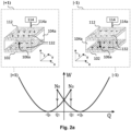
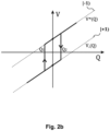
- Fig. 2a , Fig. 2b refer to the situation of a single ferroelectric nanoparticle 104a between conductive elements 102, 112, with a charge control device 114 electrically connected 114a to one of the conductive elements 102, 112.
- the ferroelectric nanoparticle 104a is uniformly polarized and is confined between the two conductive elements 102, 112 carrying the electric charge 132. It can stay in either of two individual (ferroelectric) polarization states 106a: a state (+1), having the polarization directed "up” along the z-axis, and a state (-1) having the polarization directed "down".
- the single ferroelectric nanoparticle 104a between conductive elements 102, 112 thus implements two corresponding logical levels,
- the individual polarization state 106a may be controlled by the charge applied to the conductive elements 102, 112.
- the single ferroelectric nanoparticle 104a of Fig. 2a confined between the conductive elements 102, 112, therefore implements a binary (i. e., two-level) logic device with the logical levels
- a charge control device 114 with an electrical connection 114a to at least one of the conductive elements 102, 112 is used to control the charge of the respective conductive element(s) 102, 112 and thus the individual polarization state 106a of the ferroelectric nanoparticle 104a or the polarization state 106 of Fig. 1 .
- This approach is distinct from conventional techniques, which control the voltages at conductive elements.
- the nanoparticle 104a or the nanoparticles 104a, 104b of Fig. 1 and their respective polarization states 106a, 106 are addressed much more reliably than in conventional techniques based on the voltage control.
- P s refers to the spontaneous polarization of the ferroelectric nanoparticle associated with the polarization state 106a.
- the terminal points N 0 (corresponding to the critical charges Q 1,2 ) of parabolas correspond to the situation where a polarization states 106a with a given polarization direction becomes unstable with respect to switching to the polarization states 106a with the opposite polarization direction.
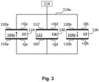
- Fig. 3 shows an effective electric circuit of the ferroelectric nanoparticle capacitor-device 100 of Fig. 1 .
- the ferroelectric nanoparticle capacitor-device 100 includes the two ferroelectric capacitors 124, 126, each with a capacitance Cf. It further comprises a dielectric capacitor 130 with a capacitance Cd, connected in parallel to the ferroelectric capacitors 124, 126.
- the effective electric circuit further comprises a charge-control element 114 in electrical contact 114a with at least one of the conductive elements 102, 112.
- the charge-control element 114 is adapted to apply a charge Q to the conductive element(s) 102, 112 it is connected to.
- the charge Q applied to the conductive elements 102, 112 can be distributed nonuniformly over the conductive elements 102, 112, forming the charge Q a in the region of the first ferroelectric nanoparticle 104a (or on first first sections 110a, 120a of the conductive elements 102, 112 corresponding to the first ferroelectric capacitor 124, respectively), the charge Q b in the region of the second ferroelectric nanoparticle 104b (or on sections 110b, 120b of the conductive elements 102, 112 corresponding to the second ferroelectric capacitor 126, respectively), and the charge Q d in the region of the dielectric material 130 (or on the second portions or the excess portions 102', 112' of the conductive layers 102, 112, respectively, corresponding to the dielectric capacitor 130).
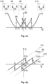
- Fig. 4a illustrates the emerging polarization states 106 and their total energies W.
- level refers to a logical level, the two terms are used equivalently.
- the levels are represented by the polarization states 106 of the ferroelectric nanoparticles 104a, 104b, and vice versa.
- the polarization states 106 provide the levels.
- the terms "level” and “polarization states” may be used equivalently.
- the polarization states 106 are preferentially discrete polarization states 106, e. g. in a sense that a switching between two different polarization states 106 is characterized by a subtle, abrupt change of the ferroelectric polarization.
- the ferroelectric nanoparticles 104a, 104b are adapted to not assume any stable ferroelectric polarization between the one of the discrete polarization states 106.
- the switching between the logical levels takes place when the field inside the corresponding ferroelectric nanoparticle 104a, 104b exceeds the coercive field Ec.
- Fig. 4a , Fig. 5a , and Fig. 6a present the abovementioned energy profiles, W +1 ( Q ) , W o (Q), W - 1 ( Q ) for the polarization states 106,
- Fig. 4b , Fig. 5b , and Fig. 6b present corresponding three-branch hysteresis loops, and routes for addressing the polarization states 106,
- Fig. 4a, Fig. 4b , Fig. 5a, Fig. 5b , Fig. 6a, and Fig. 6b represent the three existing distinct regimes of topology of the hysteresis loops, determined by the relative strength of the effective charge parameters Qc and Qs.
- +1) and transition sequence are exemplified in Fig. 4a, Fig. 4b for the case 3 Q s > Q c > 2Q s .
- the terminal points, N 0 correspond to the switching instability of one of the ferroelectric nanoparticles 104a, 104b towards the lowest-energy state with the opposite polarization 106.
- +1) at the said critical charges Q 1 , Q 2 , Q 3 , and Q 4 is demonstrated in Fig. 4b .
- Fig. 5a, Fig. 5b present the energy profile and charge-voltage characteristics realized under the condition Q c > 3 Q s .
- o is topologically unstable in a sense that once the switching from this logical level to either
- o), can be achieved, however, by variation of external parameters, different from the charge, for instance by thermal cycling, involving passing through a high temperature paraelectric state.
- Fig. 6a and Fig. 6b present the energy profiles and charge-voltage characteristics realized under the condition Q c ⁇ 2 Q s .
- Fig. 4b Fig. 4a
- Fig. 5b Fig. 5a
- Fig. 6b Fig. 6a
- the specific switching properties/protocols can be achieved by the selection of the desirable ratio between parameters, Qs and Qc , or by appropriately selecting the size and material composition of the ferroelectric nanoparticles 104a, 104b, respectively.
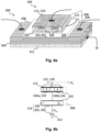
- the ferroelectric nanoparticle capacitor-device 100 of Fig. 7a is formed with various modifications: It comprises a charge control device 104, consisting of an additional conductive element 202 and a dielectric spacer 204.
- the ferroelectric nanoparticle capacitor-device 100 of Fig. 7a comprises a temperature-control element 206. It also comprises a force-control element 210.
- the ferroelectric nanoparticle capacitor-device 100 is formed with any, any combination, or all of the described modifications (charge control device 104 and/or temperature-control element 206 and/or force-control element 210).
- the charge control device 104 further comprises a dielectric spacer 204, formed as a layer 204 of dielectric material between the first conductive element 102 and the additional conductive element 202 to electrically insulate them from each other.
- the dielectric spacer 204 is composed of one of the dielectric materials described above, and preferentially contains SrTiO3, SiO2, Si3N4, or HfO2.
- the charge control device 104 is operated by applying a voltage between the additional conductive element 202 and the second conductive element 112 while the first conductive element 102 is kept at a fixed charge (e. g., electrically floating), resulting in the application of a charge to the second conductive element 112.
- a fixed charge e. g., electrically floating
- the temperature-control element 206 is implemented as a heater 206, more specifically as an Ohmic heater 206.
- the heater 206 is arranged below a conductive element 102, 112, to heat the respective conductive element 102, 112 and thus the ferroelectric nanoparticles 104a, 104b.
- a temperature variation of the ferroelectric nanoparticles 104a, 104b can be of the range 10 - 300 Kelvin.
- the ferroelectric nanoparticle capacitor-device 100 of Fig. 7a further comprises a substrate 208 to support the ferroelectric nanoparticle capacitor-device 100.
- the substrate is arranged below the conductive elements 102, 112, and below the additional conductive element 202 if present.
- the substrate is in thermal contact with one of the (first, second, or additional) conductive elements 102, 112, 202; e. g. via a direct physical contact or an indirect contact via a heat-conducting material such as a metal or a sufficiently thin ( ⁇ 100 nm or ⁇ 20 nm) intermediate layer.
- Heating the substrate 208 using the heater 223 leads to a mechanical deformation 212 in the form of an expansion 212, that generates strains in the ferroelectric nanoparticles 104a, 104b.
- the strain can also be induced by the piezoelectric effect developing when the electric field is applied to the substrate 208.
- the generated strain can lie in the range of 0.001-0.1% of the crystal lattice constant.
- the temperature-control element 206 and/or the force-control element 210 permit to tune the interrelation between the parameters Qs and Qc by the external stimuli temperature and/or strain. They thus allow for an on-the-fly modification of the switching logic of the said device 100. This tuning can be done by accounting for different temperature and strain dependences of these parameters.
- the so-called hyperelectric materials for example, LiZnAs, LiBeSb, NaZnSb, and LiBeBi, present the particular interest for implementation of the ferroelectric nanoparticles 104a, 104b, because in these materials the coercive field can achieve values substantially larger than the depolarization electric field, and the relative strengths of the parameters, Qs and Qc can vary over fairly wide ranges.
- Fig. 7b shows an equivalent electric circuit of the ferroelectric nanoparticle capacitor-device 100 of Fig. 7a .
- the additional conductive element 202 and the dielectric spacer 204 form an additional capacitor 214 with the capacitance Ci.
- the additional capacitor 214 shares the first conductive element 102 with the capacitors 124, 126, 130.
- the equivalent electric circuit therefore comprises the capacitors 124, 126, 130 (defined by the conductive elements 102, 112) and the additional capacitor 214 (defined by the conductive elements 102, 202) connected in series.
- the second conductive element 112 and the additional conductive element 202 receive the incoming voltage Vin between them.
- This relation becomes particularly simple and transforms to Q ⁇ Ci Vin when the effective capacitance of the parallel arrangement of the capacitors 124, 126, 130 substantially exceeds the capacitance of the additional capacitor 214.
- the charge that controls the polarization state 106 of the ferroelectric nanoparticles 104a, 104b is directly tuned by the voltage Vin applied to the second conductive element 112 and the additional conductive element 202.
- Fig. 8a illustrates the integration of the ferroelectric nanoparticle capacitor-device 100 into a field-effect transistor 300, alternatively implementing the hysteresis loops shown in Fig. 4b (Fig. 4a ), Fig. 5b (Fig. 5a ) and Fig. 6b (Fig. 6a ).
- Fig. 8b shows an equivalent electric circuit of the device 100 of Fig. 8a .
- the field-effect transistor 300 comprises source/drain regions 304, 306, a channel 302 extending between the source/drain regions 304, 306, and a gate stack 308 arranged over the channel 302.
- the field-effect transistor 300 further comprises a body electrode 312, which is grounded.
- the channel 302 serves as the additional conductive element 202 described in the context of Fig. 8a .
- the gate dielectric 204 is a high- ⁇ dielectric layer, preventing a charge leakage between the first conductive element 102 and the channel 302.
- the gate stack comprises the gate dielectric 204, provided by the dielectric spacer 204, and at least one electrode.
- the at least one electrode of the gate stack 308 is provided by a ferroelectric nanoparticle capacitor-device 100 similar to the one of Fig. 1 .
- the second conductive element 112 of the ferroelectric nanoparticle capacitor-device 100 serves as a gate electrode of the transistor 300 and is connected to an external voltage source to receive the driving voltage V in .
- the driving voltage V in is applied between the second conductive element 112 and the additional conductive element (channel) 202, 302, implementing the charge control device 114 described above in the context of Fig. 7a .
- the first conductive element 102 is kept at a constant charge, e. g. kept electrically isolated and floating. It thus serves to stabilize the polarization 106 of the ferroelectric nanoparticles 104a, 104b. Furthermore, the floating first conductive element 102 makes the potential along the interface between the ferroelectric nanoparticles 104a, 104b and the first conductive element 102 even, maintaining, therefore, a uniform electric field across the gate stack 308 and the substrate 304.
- the stepwise switching of the voltage, V out , operating the current in the channel 302, under the appropriate protocol for the variation of the driving voltage V in realizes the multilevel logic switching sequence corresponding to the one of the topologically possible hysteresis loops (see Fig. 4a to Fig. 6b ).
- the logic levels switching order can be modified by the external stimuli, for example, by the temperature or strain, as described above in the context of Fig. 7a, Fig. 7b , allowing for the on-fly modification of the switching logics of the ferroelectric nanoparticle capacitor-device 100.
- the ferroelectric nanoparticle capacitor-device 100 is formed with the temperature-control element 206 and/or the force-control element 210 described above in the context of Fig. 7a , e. g. instead of the substrate 312, integrated into the substrate 312 or below the substrate 312. In the latter embodiments, a substrate 312 with a high heat conductivity is applied.
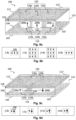
- Fig. 9a, Fig. 9c present embodiments of the ferroelectric nanoparticle capacitor-device 100 for implementing a topologically configurable 4-level logical unit.
- Fig. 9b, Fig. 9d show the respective polarization states 106 representing the 4 logical levels.
- Fig. 9a shows a ferroelectric nanoparticle capacitor-device 100 with three identical, for example, cylindrical ferroelectric nanoparticles 104a, 104b, 104c between the conductive elements 102, 112.
- the ferroelectric nanoparticles 104a, 104b, 104c provide equal coercive fields and equal cross-sections.
- a dielectric separator material 122 fills the residual space between the conductive elements 102, 114.
- the system is driven and controlled by an electric charge, Q, placed onto at least one of the conductive elements 102, 114, using a charge control element 114 as described above.
- the ferroelectric nanoparticle capacitor-device 100 of Fig. 9a provides the polarization states, (+++), (++-) (or equivalently, (+-+) and (-++)), (+--), or equivalently, (-+-) and (--+), and, finally, (---), wherein arrows down (or up) in Fig. 9b represent negative "-" or positive "+” polarization with respect to the z axis.
- ferroelectric nanoparticle capacitor-device 100 of Fig. 9a realizes a 4-level logic, characterized by the logic levels
- Fig. 9c shows another embodiment of a ferroelectric nanoparticle capacitor-device 100 for implementing a 4-level logic device.
- two non-equivalent ferroelectric nanoparticles 104a, 104b are disposed between the conductive elements 102, 112 and coated by a dielectric separator material 122.
- the ferroelectric nanoparticles 104a, 104b can be made from different ferroelectric materials and may have different sizes.
- Fig. 9d illustrates the polarization states 106 of the ferroelectric nanoparticles 104a, 104b of Fig. 9c , which are similar to the polarization states 106 of Fig. 4a associated with the ferroelectric nanoparticles 104a, 104b, 104c of Fig. 1 .
- the four polarization states 106 implement the logical levels of a 4-level logic unit, namely, (--) ⁇
- the embodiments of Fig. 9a, Fig. 9c are similar to the embodiment of Fig. 1 .
- the ferroelectric nanoparticles 104a, 104b, 104c described in the context of Fig. 9a or Fig. 9c are applied in a ferroelectric nanoparticle capacitor-device 100 similar to the embodiment of Fig. 7a or Fig. 8a .
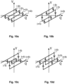
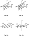
- Fig. 10a, Fig. 10b, Fig. 10c, Fig. 10d , Fig. 10e, Fig. 10f, Fig. 10g, and Fig. 10h illustrate charge-voltage hysteresis loops associated with the polarization states 106 of ferroelectric nanoparticle capacitor-devices 100 similar to the ones of Fig. 9a or Fig. 9c .
- Fig. 10a shows a charge-voltage hysteresis loop with the sequential switching between the logical levels/polarization states 106,
- the charge-voltage hysteresis loops in Fig. 10a, Fig. 10b, Fig. 10c, and Fig. 10d correspond to different switching sequences between logical levels/polarization states 106,
- the charge-voltage hysteresis loops of Fig. 10e and Fig. 10f comprise "hidden” logical levels
- Such protocols can be used if the information, stored at the "hidden levels”
- the charge-voltage hysteresis loops of Fig. 10g and Fig. 10h implement the multilevel Schmitt trigger, required for multiple applications in electronics.
- the ferroelectric nanoparticle capacitor-device 100 of Fig. 9a or 9c via selection of appropriate sizes and material compositions of the ferroelectric nanoparticles 104a, 104b, 104c, enables the implementation of any preselected charge-voltage hysteresis loop of the charge-voltage hysteresis loops represented in Fig. 10a, Fig. 10b, Fig. 10c, Fig. 10d , Fig. 10e, Fig. 10f, Fig. 10g, and Fig. 10h .
- Controlling external stimuli for instance, the temperature or strain, as described above in the context of Fig. 7a , Fig. 8b , the charge-voltage hysteresis loop and the switching sequence between the logical levels/polarization states 106,
- -2) can be selected and modified on-the-fly, i. e. after fabrication of the ferroelectric nanoparticle capacitor-device 100 with given sizes and material compositions of the ferroelectric nanoparticles 104a, 104b, 104c.
- the charge-voltage hysteresis loop can be controlled for a ferroelectric nanoparticle capacitor-device 100 comprising more than three, for example, four, five, or any larger number of ferroelectric nanoparticles104a, 104b, 104c.
- the charge-voltage hysteresis loop can be controlled initially via selection of an appropriate number of appropriate ferroelectric nanoparticles 104a, 104b, 104c and their sizes and material compositions. A later, on-the-fly control is achieved by incorporating a temperature-control element 206 or a force-control element as described above.
- a smaller number of ferroelectric nanoparticles 104a, 104b, 104c such as up to 10, 5, 4 or three ferroelectric nanoparticles104a, 104b, 104c is preferable.
- the number of polarization states 106 should be limited, e. g. to up to 64, 32, 16, 8, or 5 polarization states 106.
- a smaller number of ferroelectric nanoparticles 104a, 104b, 104c and/or number of polarization states 106 improves the reliability of the switching and of the readout of the polarization state 106.
- Embodiments with more than three ferroelectric nanoparticles 104a, 104b, 104c use the (ferroelectric and/or dielectric) materials described above, as well as the temperature and/or strain ranges described above; also the remaining device parameters are similar to the ones described above.
- Devices comprising any other number of the nanoparticles and their configuration realize multilevel logic units possessing more complicated routes for the charge-voltage hysteresis loops enabling, therefore, even higher levels of the neuromorphic computing.
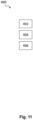
- Fig. 11 illustrates a method 400 for operating the ferroelectric nanoparticle capacitor-device 100.
- the ferroelectric nanoparticle capacitor-device 100 is similar to one of the ferroelectric nanoparticle capacitor-devices 100 described above in the context of Fig. 1 , Fig. 7a , Fig. 8a , Fig. 9a, or Fig. 9c . Any of those ferroelectric nanoparticle capacitor-devices 100 provides a maximum-ferroelectric-polarization state (and a minimum-ferroelectric-polarization state) with a maximum (and a minimum) ferroelectric polarization, such that no polarization state of the at least three polarization states has a ferroelectric polarization larger (or smaller, respectively) than the maximum-ferroelectric-polarization state (or the minimum-ferroelectric-polarization state). Moreover, any of those ferroelectric nanoparticle capacitor-devices 100 provides an intermediate-ferroelectric-polarization state with a polarization between the minimum ferroelectric polarization and the maximum ferroelectric polarization.
- the method 400 comprises selecting an intermediate-ferroelectric-polarization state.
- the method 400 comprises selecting a first voltage or charge according to the selected intermediate-ferroelectric-polarization state.
- the method 400 comprises applying the first voltage or charge to a conductive element 102, 112 of the pair to set the ferroelectric nanoparticles 104a, 104b, 104c to the selected intermediate-ferroelectric-polarization state.
- the current polarization state 106 of the ferroelectric nanoparticles 104a, 104b, 104c is detected based on a voltage of at least one of the conductive elements 102, 112.
- the voltage between the conductive elements 102, 112 is measured, which corresponds to the voltage in the charge-voltage hysteresis loop described above.
- the measured voltage is thus directly associated with the polarization state 106.
- the current polarization state 106 of the ferroelectric nanoparticles 104a, 104b, 104c is detected based on a change of the voltage of at least one of the conductive elements 102, 112, such as by counting jumps of the voltage of at least one of the conductive elements 102, 112.
- the voltage measurement is performed continuously to identify the change of the voltage.
- the other conductive element 102, 112 of the pair is kept at a constant electrical charge.
- the first voltage or charge is applied between one of the conductive elements (i. e., the second conductive element 112 described above) and the additional conductive element 202, 302 described above, preferably using the charge control device 114 described above.
- a ferroelectric nanoparticle capacitor-device 100 with a charge-voltage hysteresis loop as illustrated in Fig. 10a When applied to a ferroelectric nanoparticle capacitor-device 100 with a charge-voltage hysteresis loop as illustrated in Fig. 10a , the voltage or charge applied to the conductive element 102, 112 is continuously increased until the first voltage or charge is reached. To reach a polarization state 106 with a larger or smaller (i. e., more negative) polarization, a larger or smaller voltage or charge is applied to the conductive element 102, 112.
- the ferroelectric nanoparticle capacitor-device 100 thus implements a non-volatile memory, which can be used to store information without external power, voltage, or charge support.
- the voltage or charge applied to the conductive element 102, 112 When applied to a ferroelectric nanoparticle capacitor-device 100 with a charge-voltage hysteresis loop as illustrated in Fig. 10b , to reach the intermediate-ferroelectric-polarization state
- the voltage or charge applied to the conductive element 102, 112 first needs to be increased to a positive value sufficient to reach state
- a ferroelectric nanoparticle capacitor-device 100 with a "hidden state" such as illustrated in the context of Fig. 5b , Fig. 10e, Fig. 10f .
- heating the ferroelectric nanoparticles 104a, 104b, 104c and/or applying a mechanical force to the ferroelectric nanoparticles 104a, 104b, 104c can be used to set the polarization state 106 of the ferroelectric nanoparticles 104a, 104b, 104c to the hidden state.
- heating the ferroelectric nanoparticles 104a, 104b, 104c and/or applying a mechanical force to the ferroelectric nanoparticles 104a, 104b, 104c is used to modify the charge-voltage hysteresis loop of the ferroelectric nanoparticle capacitor-device 100.
Landscapes
- Engineering & Computer Science (AREA)
- Power Engineering (AREA)
- Physics & Mathematics (AREA)
- Theoretical Computer Science (AREA)
- Computer Hardware Design (AREA)
- Health & Medical Sciences (AREA)
- Life Sciences & Earth Sciences (AREA)
- Biomedical Technology (AREA)
- Biophysics (AREA)
- Mathematical Physics (AREA)
- General Health & Medical Sciences (AREA)
- Molecular Biology (AREA)
- Computing Systems (AREA)
- General Engineering & Computer Science (AREA)
- General Physics & Mathematics (AREA)
- Software Systems (AREA)
- Data Mining & Analysis (AREA)
- Computational Linguistics (AREA)
- Artificial Intelligence (AREA)
- Evolutionary Computation (AREA)
- Microelectronics & Electronic Packaging (AREA)
- Neurology (AREA)
- Manufacturing & Machinery (AREA)
- Chemical & Material Sciences (AREA)
- Inorganic Chemistry (AREA)
- Semiconductor Memories (AREA)
- Materials Engineering (AREA)
- Formation Of Insulating Films (AREA)
- Semiconductor Integrated Circuits (AREA)
Claims (15)
- Ferroelektrikumsnanopartikel-Kondensatorvorrichtung (100), umfassend:ein Paar von leitfähigen Elementen (102, 112), die elektrisch voneinander isoliert sind, wobei ein erstes leitfähiges Element (102) des Paars elektrisch potentialfrei ist;eine Ladungssteuervorrichtung (114), die dazu ausgelegt ist, eine Ladung auf einem zweiten leitfähigen Element (112) des Paars zu ändern; undferroelektrische Nanopartikel (104a, 104b), die zwischen den leitfähigen Elementen (102, 112) des Paars angeordnet und die dazu eingerichtet sind, einzelne Polarisationszustände bereitzustellen;wobei die ferroelektrischen Nanopartikel (104a, 104b) dazu eingerichtet sind, mindestens drei Polarisationszustände (106) mit unterschiedlichen ferroelektrischen Gesamtpolarisationen bereitzustellen, wobei sich die mindestens drei Polarisationszustände (106) auf Kombinationen der einzelnen Polarisationszustände der ferroelektrischen Nanopartikel (104a, 104b) beziehen;wobei die Ladungssteuervorrichtung (114) ein zusätzliches leitfähiges Element (202) aufweist, das elektrisch von dem Paar von leitfähigen Elementen (102, 112) isoliert ist; undwobei die Ladungssteuervorrichtung (114) dazu eingerichtet ist, eine Spannung zwischen dem zusätzlichen leitfähigen Element (202) und dem zweiten leitfähigen Element (112) anzulegen.
- Ferroelektrikumsnanopartikel-Kondensatorvorrichtung (100) nach Anspruch 1, wobei drei ferroelektrische Nanopartikel (104a, 104b) zwischen den leitfähigen Elementen (102, 112) des Paars angeordnet sind.
- Ferroelektrikumsnanopartikel-Kondensatorvorrichtung (100) nach Anspruch 1 oder 2,wobei die leitfähigen Elemente (102, 112) des Paars jeweils Oberflächen (108, 118) aufweisen, die einander zugewandt sind, undwobei Oberflächenflächen der Oberflächen (108, 118) jeweils eine Fläche einer Projektion der ferroelektrischen Nanopartikel (104a, 104b) auf eine der Oberflächen (110, 120) überschreiten.
- Ferroelektrikumsnanopartikel-Kondensatorvorrichtung (100) nach einem der vorhergehenden Ansprüche, wobei die ferroelektrischen Partikel (104a, 104b) voneinander beabstandet sind und/oder wobei ein dielektrisches Trennmaterial (122) zwischen den ferroelektrischen Nanopartikeln (104a, 104b) angeordnet ist.
- Ferroelektrikumsnanopartikel-Kondensatorvorrichtung (100) nach einem der vorhergehenden Ansprüche,wobei ein erster ferroelektrischer Nanopartikel (104a) der ferroelektrischen Nanopartikel (104a, 104b) eine erste Größe aufweist,wobei ein zweiter ferroelektrischer Nanopartikel (104b) der ferroelektrischen Nanopartikel (104a, 104b) eine zweite Größe aufweist, undwobei die erste Größe größer als die zweite Größe ist.
- Ferroelektrikumsnanopartikel-Kondensatorvorrichtung (100) nach einem der vorhergehenden Ansprüche, wobei jeweilige Größen der ferroelektrischen Nanopartikel entlang jeder beliebigen Richtung 30 nm nicht überschreiten.
- Ferroelektrikumsnanopartikel-Kondensatorvorrichtung (100) nach einem der vorhergehenden Ansprüche, wobei die ferroelektrischen Nanopartikel (104a, 104b) jeweils monodomänige ferroelektrische Zustände aufweisen.
- Ferroelektrikumsnanopartikel-Kondensatorvorrichtung (100) nach einem der vorhergehenden Ansprüche, wobei das zusätzliche leitfähige Element (202) und das zweite leitfähige Element (112) auf entgegengesetzten Seiten des ersten leitfähigen Elements (102) angeordnet sind.
- Ferroelektrikumsnanopartikel-Kondensatorvorrichtung (100) nach einem der vorhergehenden Ansprüche, ferner aufweisend einen Transistor (300), wobei ein Kanal des Transistors (300) das erste leitfähige Element (102) oder das zweite leitfähige Element (112) bildet.
- Ferroelektrikumsnanopartikel-Kondensatorvorrichtung (100) nach Anspruch 9, wobei das zusätzliche leitfähige Element (202) von dem ersten leitfähigen Element (102) durch einen dielektrischen Abstandshalter (204) getrennt ist, und wobei der dielektrische Abstandshalter (204) ein Gate-Dielektrikum des Transistors (300) bildet.
- Ferroelektrikumsnanopartikel-Kondensatorvorrichtung (100) nach einem der vorhergehenden Ansprüche, ferner aufweisend:ein Temperatursteuerelement (206), das dazu eingerichtet ist, eine Temperatur der ferroelektrischen Nanopartikel (104a, 104b) zu steuern und/oder zu ändern; und/oderein Kraftsteuerelement (210), das dazu eingerichtet ist, eine auf die ferroelektrischen Nanopartikel (104a, 104b) ausgeübte mechanische Kraft zu steuern und/oder zu ändern.
- Verwendung der Ferroelektrikumsnanopartikel-Kondensatorvorrichtung (100) nach einem der vorhergehenden Ansprüche als eine Datenspeichervorrichtung mit mehreren logischen Levels.
- Verfahren (400) zum Betreiben einer Ferroelektrikumsnanopartikel-Kondensatorvorrichtung (100),
wobei die Ferroelektrikumsnanopartikel-Kondensatorvorrichtung (100) aufweist:ein Paar von leitfähigen Elementen (102a, 112), die elektrisch voneinander isoliert sind, undferroelektrische Nanopartikel (104a, 104b), die zwischen den leitfähigen Elementen (104a, 104b) des Paars angeordnet und dazu eingerichtet sind, einzelne Polarisationszustände bereitzustellen;wobei die ferroelektrischen Nanopartikel (104a, 104b) dazu eingerichtet sind, mindestens drei Polarisationszustände (106) mit unterschiedlichen ferroelektrischen Gesamtpolarisationen bereitzustellen, umfassend einen Zustand mit einer geringsten ferroelektrischen Polarisation, einen Zustand mit einer größten ferroelektrischen Polarisation und mindestens einen Zustand mit einer dazwischenliegenden ferroelektrischen Polarisation, wobei sich die mindestens drei Polarisationszustände (106) auf Kombinationen der einzelnen Polarisationszustände der ferroelektrischen Nanopartikel (104a, 104b) beziehen;wobei das Verfahren (400) umfasst:Auswählen (402) eines Zustands mit einer dazwischenliegenden ferroelektrischen Polarisation;Auswählen (404) einer ersten Spannung oder Ladung gemäß dem ausgewählten Zustand mit der dazwischenliegenden ferroelektrischen Polarisation;Anlegen (406) der ersten Spannung oder Ladung an ein leitfähiges Element (102, 112) des Paars, um die ferroelektrischen Nanopartikel (104a, 104b) auf den ausgewählten Zustand mit der dazwischenliegenden ferroelektrischen Polarisation einzustellen; undHalten des anderen leitfähigen Elements des Paars auf einer konstanten elektrischen Ladung. - Verfahren (400) nach Anspruch 13, ferner umfassend:
vor dem Anlegen der ersten Spannung oder Ladung, um die ferroelektrischen Nanopartikel auf den ausgewählten Zustand mit der dazwischenliegenden ferroelektrischen Polarisation einzustellen:Bereitstellen der ferroelektrischen Nanopartikel (104a, 104b) in einem ersten Polarisationszustand der mindestens drei Polarisationszustände (106), wobei sich der erste Polarisationszustand von dem ausgewählten Zustand mit der dazwischenliegenden ferroelektrischen Polarisation unterscheidet;Auswählen einer zweiten Spannung oder Ladung gemäß dem ausgewählten Zustand mit der dazwischenliegenden ferroelektrischen Polarisation und/oder gemäß dem ersten Polarisationszustand; undAnlegen der zweiten Spannung oder Ladung an das leitfähige Element (102, 112) des Paars, um die ferroelektrischen Nanopartikel (104a, 104b) von dem ersten Polarisationszustand auf einen zweiten Polarisationszustand der mindestens drei Polarisationszustände (106) einzustellen, wobei sich der zweite Polarisationszustand sowohl von dem ersten Polarisationszustand als auch von dem ausgewählten Zustand mit der dazwischenliegenden ferroelektrischen Polarisation unterscheidet. - Verfahren (400) nach Anspruch 13 oder 14,wobei der ausgewählte Zustand mit der dazwischenliegenden ferroelektrischen Polarisation ein remanenter Zustand ist, und/oderwobei das Verfahren ferner das Reduzieren der Spannung oder Ladung, die an das leitfähige Element (102, 112) angelegt wird, und dabei das Beibehalten des eingestellten Zustands mit der dazwischenliegenden ferroelektrischen Polarisation umfasst; insbesondere das Reduzieren der Spannung um mindestens 30 %, um mindestens einen Faktor von 2, um mindestens einen Faktor von 3, um mindestens einen Faktor von 5, um mindestens einen Faktor von 10 oder um mindestens einen Faktor von 100.
Priority Applications (15)
| Application Number | Priority Date | Filing Date | Title |
|---|---|---|---|
| EP22200942.5A EP4354477B1 (de) | 2022-10-11 | 2022-10-11 | Ferroelektrischer nanopartikelkondensator für nichtbinäre logik |
| EP23197777.8A EP4354478A3 (de) | 2022-10-11 | 2023-09-15 | Ferroelektrischer nanopartikelkondensator für nichtbinäre logik und betriebsverfahren |
| AU2023237205A AU2023237205B2 (en) | 2022-10-11 | 2023-10-02 | Ferroelectric nanoparticle capacitor for non-binary logics |
| JP2023171178A JP7671520B2 (ja) | 2022-10-11 | 2023-10-02 | 非二元論理用の強誘電体ナノ粒子キャパシタ |
| AU2023241268A AU2023241268B2 (en) | 2022-10-11 | 2023-10-03 | Ferroelectric nanoparticle capacitor for non-binary logics and method of operation |
| JP2023172114A JP7724559B2 (ja) | 2022-10-11 | 2023-10-03 | 非二元論理用の強誘電体ナノ粒子キャパシタおよび動作方法 |
| US18/376,788 US20240120366A1 (en) | 2022-10-11 | 2023-10-04 | Ferroelectric nanoparticle capacitor for non-binary logics |
| US18/376,762 US12527001B2 (en) | 2022-10-11 | 2023-10-04 | Ferroelectric nanoparticle capacitor for non-binary logics and method of operation |
| CA3215456A CA3215456A1 (en) | 2022-10-11 | 2023-10-04 | Ferroelectric nanoparticle capacitor for non-binary logics and method of operation |
| CA3215597A CA3215597A1 (en) | 2022-10-11 | 2023-10-04 | Ferroelectric nanoparticle capacitor for non-binary logics |
| KR1020230134798A KR102884992B1 (ko) | 2022-10-11 | 2023-10-11 | 비-이진 로직들을 위한 강유전체 나노입자 커패시터 |
| CN202311313432.3A CN117878102A (zh) | 2022-10-11 | 2023-10-11 | 用于非二值逻辑的铁电纳米颗粒电容器及操作方法 |
| KR1020230134800A KR102866049B1 (ko) | 2022-10-11 | 2023-10-11 | 비-이진 로직들을 위한 강유전체 나노입자 커패시터 및 동작 방법 |
| CN202311312587.5A CN117878101A (zh) | 2022-10-11 | 2023-10-11 | 用于非二值逻辑的铁电纳米颗粒电容器 |
| KR1020250136178A KR20250143294A (ko) | 2022-10-11 | 2025-09-22 | 비-이진 로직들을 위한 강유전체 나노입자 커패시터 및 동작 방법 |
Applications Claiming Priority (1)
| Application Number | Priority Date | Filing Date | Title |
|---|---|---|---|
| EP22200942.5A EP4354477B1 (de) | 2022-10-11 | 2022-10-11 | Ferroelektrischer nanopartikelkondensator für nichtbinäre logik |
Publications (3)
| Publication Number | Publication Date |
|---|---|
| EP4354477A1 EP4354477A1 (de) | 2024-04-17 |
| EP4354477C0 EP4354477C0 (de) | 2025-03-19 |
| EP4354477B1 true EP4354477B1 (de) | 2025-03-19 |
Family
ID=83690109
Family Applications (2)
| Application Number | Title | Priority Date | Filing Date |
|---|---|---|---|
| EP22200942.5A Active EP4354477B1 (de) | 2022-10-11 | 2022-10-11 | Ferroelektrischer nanopartikelkondensator für nichtbinäre logik |
| EP23197777.8A Pending EP4354478A3 (de) | 2022-10-11 | 2023-09-15 | Ferroelektrischer nanopartikelkondensator für nichtbinäre logik und betriebsverfahren |
Family Applications After (1)
| Application Number | Title | Priority Date | Filing Date |
|---|---|---|---|
| EP23197777.8A Pending EP4354478A3 (de) | 2022-10-11 | 2023-09-15 | Ferroelektrischer nanopartikelkondensator für nichtbinäre logik und betriebsverfahren |
Country Status (7)
| Country | Link |
|---|---|
| US (2) | US12527001B2 (de) |
| EP (2) | EP4354477B1 (de) |
| JP (2) | JP7671520B2 (de) |
| KR (3) | KR102866049B1 (de) |
| CN (2) | CN117878101A (de) |
| AU (2) | AU2023237205B2 (de) |
| CA (2) | CA3215597A1 (de) |
Family Cites Families (19)
| Publication number | Priority date | Publication date | Assignee | Title |
|---|---|---|---|---|
| JPH07122661A (ja) * | 1993-10-27 | 1995-05-12 | Olympus Optical Co Ltd | 強誘電体メモリ装置 |
| US6316797B1 (en) * | 1999-02-19 | 2001-11-13 | Advanced Technology Materials, Inc. | Scalable lead zirconium titanate(PZT) thin film material and deposition method, and ferroelectric memory device structures comprising such thin film material |
| TW571403B (en) * | 2001-06-22 | 2004-01-11 | Matsushita Electric Industrial Co Ltd | Semiconductor device and the driving method |
| JP2003163332A (ja) * | 2001-06-22 | 2003-06-06 | Matsushita Electric Ind Co Ltd | 半導体装置 |
| JP2006269611A (ja) * | 2005-03-23 | 2006-10-05 | Seiko Epson Corp | 半導体装置、半導体パッケージ装置、強誘電体キャパシタの再生方法、強誘電体メモリ装置の初期化方法、および強誘電体メモリ装置の廃却方法 |
| JP4671037B2 (ja) * | 2005-12-20 | 2011-04-13 | セイコーエプソン株式会社 | 記憶装置 |
| JP2010080520A (ja) * | 2008-09-24 | 2010-04-08 | Toshiba Corp | 半導体記憶装置およびその製造方法 |
| KR101300241B1 (ko) * | 2011-08-31 | 2013-08-26 | 서울대학교산학협력단 | 강유전체 메모리 소자 및 그의 제조 방법 |
| KR101429160B1 (ko) * | 2013-06-21 | 2014-09-23 | 한국과학기술원 | 멀티비트 메모리 소자 |
| FR3030115B1 (fr) * | 2014-12-10 | 2017-12-15 | Commissariat Energie Atomique | Condensateur a capacite variable comprenant une couche de materiau a changement d'etat et un procede de variation d'une capacite d'un condensateur |
| US10783430B2 (en) | 2016-09-26 | 2020-09-22 | The Boeing Company | Signal removal to examine a spectrum of another signal |
| US10038092B1 (en) * | 2017-05-24 | 2018-07-31 | Sandisk Technologies Llc | Three-level ferroelectric memory cell using band alignment engineering |
| JP2019169574A (ja) * | 2018-03-23 | 2019-10-03 | 東芝メモリ株式会社 | 半導体記憶装置 |
| US10679688B2 (en) * | 2018-04-16 | 2020-06-09 | Samsung Electronics Co., Ltd. | Ferroelectric-based memory cell usable in on-logic chip memory |
| JP7066585B2 (ja) * | 2018-09-19 | 2022-05-13 | キオクシア株式会社 | 記憶装置 |
| US11296099B2 (en) * | 2019-07-31 | 2022-04-05 | Taiwan Semiconductor Manufacturing Company, Ltd. | FeRAM decoupling capacitor |
| US11380708B2 (en) * | 2019-08-30 | 2022-07-05 | Taiwan Semiconductor Manufacturing Company, Ltd. | Analog non-volatile memory device using poly ferroelectric film with random polarization directions |
| US11532355B2 (en) * | 2019-09-26 | 2022-12-20 | The Regents Of The University Of California | Non-volatile multi-level cell memory using a ferroelectric superlattice and related systems |
| US11430510B2 (en) * | 2020-12-11 | 2022-08-30 | International Business Machines Corporation | Multi-level ferroelectric field-effect transistor devices |
-
2022
- 2022-10-11 EP EP22200942.5A patent/EP4354477B1/de active Active
-
2023
- 2023-09-15 EP EP23197777.8A patent/EP4354478A3/de active Pending
- 2023-10-02 JP JP2023171178A patent/JP7671520B2/ja active Active
- 2023-10-02 AU AU2023237205A patent/AU2023237205B2/en active Active
- 2023-10-03 JP JP2023172114A patent/JP7724559B2/ja active Active
- 2023-10-03 AU AU2023241268A patent/AU2023241268B2/en active Active
- 2023-10-04 CA CA3215597A patent/CA3215597A1/en active Pending
- 2023-10-04 US US18/376,762 patent/US12527001B2/en active Active
- 2023-10-04 US US18/376,788 patent/US20240120366A1/en active Pending
- 2023-10-04 CA CA3215456A patent/CA3215456A1/en active Pending
- 2023-10-11 CN CN202311312587.5A patent/CN117878101A/zh active Pending
- 2023-10-11 KR KR1020230134800A patent/KR102866049B1/ko active Active
- 2023-10-11 KR KR1020230134798A patent/KR102884992B1/ko active Active
- 2023-10-11 CN CN202311313432.3A patent/CN117878102A/zh active Pending
-
2025
- 2025-09-22 KR KR1020250136178A patent/KR20250143294A/ko active Pending
Also Published As
| Publication number | Publication date |
|---|---|
| EP4354477C0 (de) | 2025-03-19 |
| EP4354478A3 (de) | 2024-06-19 |
| US20240121967A1 (en) | 2024-04-11 |
| JP2024056635A (ja) | 2024-04-23 |
| CN117878101A (zh) | 2024-04-12 |
| CA3215456A1 (en) | 2024-04-11 |
| KR102866049B1 (ko) | 2025-09-26 |
| AU2023237205B2 (en) | 2025-03-06 |
| CN117878102A (zh) | 2024-04-12 |
| CA3215597A1 (en) | 2024-04-11 |
| JP7671520B2 (ja) | 2025-05-02 |
| JP7724559B2 (ja) | 2025-08-18 |
| AU2023237205A1 (en) | 2024-05-02 |
| AU2023241268B2 (en) | 2026-04-30 |
| KR20240050291A (ko) | 2024-04-18 |
| AU2023241268A1 (en) | 2024-05-02 |
| KR20240050290A (ko) | 2024-04-18 |
| EP4354477A1 (de) | 2024-04-17 |
| JP2024056638A (ja) | 2024-04-23 |
| EP4354478A2 (de) | 2024-04-17 |
| KR102884992B1 (ko) | 2025-11-12 |
| US12527001B2 (en) | 2026-01-13 |
| KR20250143294A (ko) | 2025-10-01 |
| US20240120366A1 (en) | 2024-04-11 |
Similar Documents
| Publication | Publication Date | Title |
|---|---|---|
| Pešić et al. | Built-in bias generation in anti-ferroelectric stacks: Methods and device applications | |
| CN110192279B (zh) | 存储器单元及形成电容器的方法 | |
| CN113948581B (zh) | 存储器单元、存储器单元布置及其方法 | |
| US11594542B2 (en) | Remanent polarizable capacitive structure, memory cell, and methods thereof | |
| KR102007391B1 (ko) | 변동 저저항 라인 비휘발성 메모리 소자 및 이의 동작 방법 | |
| US11380708B2 (en) | Analog non-volatile memory device using poly ferroelectric film with random polarization directions | |
| US20220139932A1 (en) | Memory cell, capacitive memory structure, and methods thereof | |
| US9685215B1 (en) | Semiconductor memory device including a ferroelectric layer | |
| TWI511280B (zh) | 記憶電容器 | |
| US9520445B2 (en) | Integrated non-volatile memory elements, design and use | |
| KR102395394B1 (ko) | 랜덤 분극 방향을 갖는 폴리 강유전체 막을 사용하는 아날로그 비휘발성 메모리 디바이스 | |
| CN117729841A (zh) | 半导体器件 | |
| Hwang et al. | Recent advances in ferroelectric materials, devices, and in-memory computing applications | |
| TW202220192A (zh) | 利用介面切換調變來增強之鐵電裝置 | |
| EP4354477A1 (de) | Ferroelektrischer nanopartikelkondensator für nichtbinäre logik | |
| US20250069658A1 (en) | Threshold Voltage Reduction in Memristive Devices | |
| Razumnaya et al. | Ferroelectric topologically configurable multilevel logic unit | |
| US11737375B2 (en) | Device including elements for compensating for local variability of electrostatic potential | |
| US20240162346A1 (en) | Field effect transistor, capacitor, and electronic apparatus including domain-controlled ferroelectric material | |
| KR102059485B1 (ko) | 변동 저저항 영역 기반 메모리 소자 및 이의 제어 방법 | |
| KR102218662B1 (ko) | 변동 저저항 라인 비휘발성 메모리 소자 및 이의 동작 방법 | |
| Ahn et al. | Mechanism and Evaluation of Two-Terminal Ferroelectric-Based Memristive/Memcapacitive Devices |
Legal Events
| Date | Code | Title | Description |
|---|---|---|---|
| PUAI | Public reference made under article 153(3) epc to a published international application that has entered the european phase |
Free format text: ORIGINAL CODE: 0009012 |
|
| STAA | Information on the status of an ep patent application or granted ep patent |
Free format text: STATUS: REQUEST FOR EXAMINATION WAS MADE |
|
| 17P | Request for examination filed |
Effective date: 20230824 |
|
| AK | Designated contracting states |
Kind code of ref document: A1 Designated state(s): AL AT BE BG CH CY CZ DE DK EE ES FI FR GB GR HR HU IE IS IT LI LT LU LV MC ME MK MT NL NO PL PT RO RS SE SI SK SM TR |
|
| GRAP | Despatch of communication of intention to grant a patent |
Free format text: ORIGINAL CODE: EPIDOSNIGR1 |
|
| STAA | Information on the status of an ep patent application or granted ep patent |
Free format text: STATUS: GRANT OF PATENT IS INTENDED |
|
| RIC1 | Information provided on ipc code assigned before grant |
Ipc: G11C 11/22 20060101ALI20240416BHEP Ipc: G11C 11/24 20060101ALI20240416BHEP Ipc: G11C 11/56 20060101ALI20240416BHEP Ipc: H10B 53/30 20230101ALI20240416BHEP Ipc: H10B 51/30 20230101ALI20240416BHEP Ipc: H01L 29/78 20060101ALI20240416BHEP Ipc: H01L 29/66 20060101ALI20240416BHEP Ipc: H01L 21/28 20060101ALI20240416BHEP Ipc: H01G 4/10 20060101ALI20240416BHEP Ipc: H01G 4/33 20060101ALI20240416BHEP Ipc: H01G 7/06 20060101AFI20240416BHEP |
|
| INTG | Intention to grant announced |
Effective date: 20240430 |
|
| GRAJ | Information related to disapproval of communication of intention to grant by the applicant or resumption of examination proceedings by the epo deleted |
Free format text: ORIGINAL CODE: EPIDOSDIGR1 |
|
| STAA | Information on the status of an ep patent application or granted ep patent |
Free format text: STATUS: REQUEST FOR EXAMINATION WAS MADE |
|
| STAA | Information on the status of an ep patent application or granted ep patent |
Free format text: STATUS: EXAMINATION IS IN PROGRESS |
|
| INTC | Intention to grant announced (deleted) | ||
| 17Q | First examination report despatched |
Effective date: 20240709 |
|
| GRAP | Despatch of communication of intention to grant a patent |
Free format text: ORIGINAL CODE: EPIDOSNIGR1 |
|
| STAA | Information on the status of an ep patent application or granted ep patent |
Free format text: STATUS: GRANT OF PATENT IS INTENDED |
|
| RIC1 | Information provided on ipc code assigned before grant |
Ipc: G06N 3/044 20230101ALN20240920BHEP Ipc: G06N 3/063 20230101ALI20240920BHEP Ipc: G06N 3/045 20230101ALI20240920BHEP Ipc: G11C 11/22 20060101ALI20240920BHEP Ipc: G11C 11/24 20060101ALI20240920BHEP Ipc: G11C 11/56 20060101ALI20240920BHEP Ipc: H10B 53/30 20230101ALI20240920BHEP Ipc: H10B 51/30 20230101ALI20240920BHEP Ipc: H01L 29/78 20060101ALI20240920BHEP Ipc: H01L 29/66 20060101ALI20240920BHEP Ipc: H01L 21/28 20060101ALI20240920BHEP Ipc: H01G 4/10 20060101ALI20240920BHEP Ipc: H01G 4/33 20060101ALI20240920BHEP Ipc: H01G 7/06 20060101AFI20240920BHEP |
|
| RIC1 | Information provided on ipc code assigned before grant |
Ipc: G06N 3/044 20230101ALN20241009BHEP Ipc: G06N 3/063 20230101ALI20241009BHEP Ipc: G06N 3/045 20230101ALI20241009BHEP Ipc: G11C 11/22 20060101ALI20241009BHEP Ipc: G11C 11/24 20060101ALI20241009BHEP Ipc: G11C 11/56 20060101ALI20241009BHEP Ipc: H10B 53/30 20230101ALI20241009BHEP Ipc: H10B 51/30 20230101ALI20241009BHEP Ipc: H01L 29/78 20060101ALI20241009BHEP Ipc: H01L 29/66 20060101ALI20241009BHEP Ipc: H01L 21/28 20060101ALI20241009BHEP Ipc: H01G 4/10 20060101ALI20241009BHEP Ipc: H01G 4/33 20060101ALI20241009BHEP Ipc: H01G 7/06 20060101AFI20241009BHEP |
|
| INTG | Intention to grant announced |
Effective date: 20241023 |
|
| GRAS | Grant fee paid |
Free format text: ORIGINAL CODE: EPIDOSNIGR3 |
|
| GRAA | (expected) grant |
Free format text: ORIGINAL CODE: 0009210 |
|
| STAA | Information on the status of an ep patent application or granted ep patent |
Free format text: STATUS: THE PATENT HAS BEEN GRANTED |
|
| AK | Designated contracting states |
Kind code of ref document: B1 Designated state(s): AL AT BE BG CH CY CZ DE DK EE ES FI FR GB GR HR HU IE IS IT LI LT LU LV MC ME MK MT NL NO PL PT RO RS SE SI SK SM TR |
|
| REG | Reference to a national code |
Ref country code: GB Ref legal event code: FG4D |
|
| REG | Reference to a national code |
Ref country code: CH Ref legal event code: EP |
|
| REG | Reference to a national code |
Ref country code: IE Ref legal event code: FG4D |
|
| REG | Reference to a national code |
Ref country code: DE Ref legal event code: R096 Ref document number: 602022011919 Country of ref document: DE |
|
| U01 | Request for unitary effect filed |
Effective date: 20250319 |
|
| U07 | Unitary effect registered |
Designated state(s): AT BE BG DE DK EE FI FR IT LT LU LV MT NL PT RO SE SI Effective date: 20250325 |
|
| PG25 | Lapsed in a contracting state [announced via postgrant information from national office to epo] |
Ref country code: RS Free format text: LAPSE BECAUSE OF FAILURE TO SUBMIT A TRANSLATION OF THE DESCRIPTION OR TO PAY THE FEE WITHIN THE PRESCRIBED TIME-LIMIT Effective date: 20250619 |
|
| PG25 | Lapsed in a contracting state [announced via postgrant information from national office to epo] |
Ref country code: NO Free format text: LAPSE BECAUSE OF FAILURE TO SUBMIT A TRANSLATION OF THE DESCRIPTION OR TO PAY THE FEE WITHIN THE PRESCRIBED TIME-LIMIT Effective date: 20250619 |
|
| PG25 | Lapsed in a contracting state [announced via postgrant information from national office to epo] |
Ref country code: HR Free format text: LAPSE BECAUSE OF FAILURE TO SUBMIT A TRANSLATION OF THE DESCRIPTION OR TO PAY THE FEE WITHIN THE PRESCRIBED TIME-LIMIT Effective date: 20250319 |
|
| PG25 | Lapsed in a contracting state [announced via postgrant information from national office to epo] |
Ref country code: GR Free format text: LAPSE BECAUSE OF FAILURE TO SUBMIT A TRANSLATION OF THE DESCRIPTION OR TO PAY THE FEE WITHIN THE PRESCRIBED TIME-LIMIT Effective date: 20250620 |
|
| PG25 | Lapsed in a contracting state [announced via postgrant information from national office to epo] |
Ref country code: SM Free format text: LAPSE BECAUSE OF FAILURE TO SUBMIT A TRANSLATION OF THE DESCRIPTION OR TO PAY THE FEE WITHIN THE PRESCRIBED TIME-LIMIT Effective date: 20250319 |
|
| PG25 | Lapsed in a contracting state [announced via postgrant information from national office to epo] |
Ref country code: ES Free format text: LAPSE BECAUSE OF FAILURE TO SUBMIT A TRANSLATION OF THE DESCRIPTION OR TO PAY THE FEE WITHIN THE PRESCRIBED TIME-LIMIT Effective date: 20250319 |
|
| PG25 | Lapsed in a contracting state [announced via postgrant information from national office to epo] |
Ref country code: PL Free format text: LAPSE BECAUSE OF FAILURE TO SUBMIT A TRANSLATION OF THE DESCRIPTION OR TO PAY THE FEE WITHIN THE PRESCRIBED TIME-LIMIT Effective date: 20250319 |
|
| PG25 | Lapsed in a contracting state [announced via postgrant information from national office to epo] |
Ref country code: CZ Free format text: LAPSE BECAUSE OF FAILURE TO SUBMIT A TRANSLATION OF THE DESCRIPTION OR TO PAY THE FEE WITHIN THE PRESCRIBED TIME-LIMIT Effective date: 20250319 |
|
| PG25 | Lapsed in a contracting state [announced via postgrant information from national office to epo] |
Ref country code: SK Free format text: LAPSE BECAUSE OF FAILURE TO SUBMIT A TRANSLATION OF THE DESCRIPTION OR TO PAY THE FEE WITHIN THE PRESCRIBED TIME-LIMIT Effective date: 20250319 |
|
| PG25 | Lapsed in a contracting state [announced via postgrant information from national office to epo] |
Ref country code: IS Free format text: LAPSE BECAUSE OF FAILURE TO SUBMIT A TRANSLATION OF THE DESCRIPTION OR TO PAY THE FEE WITHIN THE PRESCRIBED TIME-LIMIT Effective date: 20250719 |
|
| REG | Reference to a national code |
Ref country code: CH Ref legal event code: U11 Free format text: ST27 STATUS EVENT CODE: U-0-0-U10-U11 (AS PROVIDED BY THE NATIONAL OFFICE) Effective date: 20251101 |
|
| U20 | Renewal fee for the european patent with unitary effect paid |
Year of fee payment: 4 Effective date: 20251027 |
|
| PGFP | Annual fee paid to national office [announced via postgrant information from national office to epo] |
Ref country code: CH Payment date: 20251101 Year of fee payment: 4 |
|
| PLBE | No opposition filed within time limit |
Free format text: ORIGINAL CODE: 0009261 |
|
| STAA | Information on the status of an ep patent application or granted ep patent |
Free format text: STATUS: NO OPPOSITION FILED WITHIN TIME LIMIT |
|
| REG | Reference to a national code |
Ref country code: CH Ref legal event code: L10 Free format text: ST27 STATUS EVENT CODE: U-0-0-L10-L00 (AS PROVIDED BY THE NATIONAL OFFICE) Effective date: 20260128 |
|
| 26N | No opposition filed |
Effective date: 20251222 |