EP4300601A1 - Siliziumwafer, herstellungsverfahren eines siliziumwafers und passivierungsbehandlungslösung - Google Patents
Siliziumwafer, herstellungsverfahren eines siliziumwafers und passivierungsbehandlungslösung Download PDFInfo
- Publication number
- EP4300601A1 EP4300601A1 EP22188748.2A EP22188748A EP4300601A1 EP 4300601 A1 EP4300601 A1 EP 4300601A1 EP 22188748 A EP22188748 A EP 22188748A EP 4300601 A1 EP4300601 A1 EP 4300601A1
- Authority
- EP
- European Patent Office
- Prior art keywords
- silicon wafer
- treatment solution
- silicon
- containing compound
- fluoride
- Prior art date
- Legal status (The legal status is an assumption and is not a legal conclusion. Google has not performed a legal analysis and makes no representation as to the accuracy of the status listed.)
- Pending
Links
Images

Classifications
-
- H—ELECTRICITY
- H10—SEMICONDUCTOR DEVICES; ELECTRIC SOLID-STATE DEVICES NOT OTHERWISE PROVIDED FOR
- H10F—INORGANIC SEMICONDUCTOR DEVICES SENSITIVE TO INFRARED RADIATION, LIGHT, ELECTROMAGNETIC RADIATION OF SHORTER WAVELENGTH OR CORPUSCULAR RADIATION
- H10F71/00—Manufacture or treatment of devices covered by this subclass
- H10F71/121—The active layers comprising only Group IV materials
-
- H—ELECTRICITY
- H10—SEMICONDUCTOR DEVICES; ELECTRIC SOLID-STATE DEVICES NOT OTHERWISE PROVIDED FOR
- H10P—GENERIC PROCESSES OR APPARATUS FOR THE MANUFACTURE OR TREATMENT OF DEVICES COVERED BY CLASS H10
- H10P70/00—Cleaning of wafers, substrates or parts of devices
- H10P70/10—Cleaning before device manufacture, i.e. Begin-Of-Line process
- H10P70/15—Cleaning before device manufacture, i.e. Begin-Of-Line process by wet cleaning only
-
- C—CHEMISTRY; METALLURGY
- C01—INORGANIC CHEMISTRY
- C01B—NON-METALLIC ELEMENTS; COMPOUNDS THEREOF; METALLOIDS OR COMPOUNDS THEREOF NOT COVERED BY SUBCLASS C01C
- C01B33/00—Silicon; Compounds thereof
- C01B33/02—Silicon
-
- C—CHEMISTRY; METALLURGY
- C10—PETROLEUM, GAS OR COKE INDUSTRIES; TECHNICAL GASES CONTAINING CARBON MONOXIDE; FUELS; LUBRICANTS; PEAT
- C10M—LUBRICATING COMPOSITIONS; USE OF CHEMICAL SUBSTANCES EITHER ALONE OR AS LUBRICATING INGREDIENTS IN A LUBRICATING COMPOSITION
- C10M125/00—Lubricating compositions characterised by the additive being an inorganic material
- C10M125/18—Compounds containing halogen
-
- C—CHEMISTRY; METALLURGY
- C10—PETROLEUM, GAS OR COKE INDUSTRIES; TECHNICAL GASES CONTAINING CARBON MONOXIDE; FUELS; LUBRICANTS; PEAT
- C10M—LUBRICATING COMPOSITIONS; USE OF CHEMICAL SUBSTANCES EITHER ALONE OR AS LUBRICATING INGREDIENTS IN A LUBRICATING COMPOSITION
- C10M125/00—Lubricating compositions characterised by the additive being an inorganic material
- C10M125/20—Compounds containing nitrogen
-
- C—CHEMISTRY; METALLURGY
- C11—ANIMAL OR VEGETABLE OILS, FATS, FATTY SUBSTANCES OR WAXES; FATTY ACIDS THEREFROM; DETERGENTS; CANDLES
- C11D—DETERGENT COMPOSITIONS; USE OF SINGLE SUBSTANCES AS DETERGENTS; SOAP OR SOAP-MAKING; RESIN SOAPS; RECOVERY OF GLYCEROL
- C11D7/00—Compositions of detergents based essentially on non-surface-active compounds
- C11D7/02—Inorganic compounds
- C11D7/04—Water-soluble compounds
- C11D7/10—Salts
-
- C—CHEMISTRY; METALLURGY
- C11—ANIMAL OR VEGETABLE OILS, FATS, FATTY SUBSTANCES OR WAXES; FATTY ACIDS THEREFROM; DETERGENTS; CANDLES
- C11D—DETERGENT COMPOSITIONS; USE OF SINGLE SUBSTANCES AS DETERGENTS; SOAP OR SOAP-MAKING; RESIN SOAPS; RECOVERY OF GLYCEROL
- C11D7/00—Compositions of detergents based essentially on non-surface-active compounds
- C11D7/22—Organic compounds
- C11D7/32—Organic compounds containing nitrogen
- C11D7/3209—Amines or imines with one to four nitrogen atoms; Quaternized amines
-
- H—ELECTRICITY
- H10—SEMICONDUCTOR DEVICES; ELECTRIC SOLID-STATE DEVICES NOT OTHERWISE PROVIDED FOR
- H10F—INORGANIC SEMICONDUCTOR DEVICES SENSITIVE TO INFRARED RADIATION, LIGHT, ELECTROMAGNETIC RADIATION OF SHORTER WAVELENGTH OR CORPUSCULAR RADIATION
- H10F71/00—Manufacture or treatment of devices covered by this subclass
- H10F71/129—Passivating
-
- H—ELECTRICITY
- H10—SEMICONDUCTOR DEVICES; ELECTRIC SOLID-STATE DEVICES NOT OTHERWISE PROVIDED FOR
- H10F—INORGANIC SEMICONDUCTOR DEVICES SENSITIVE TO INFRARED RADIATION, LIGHT, ELECTROMAGNETIC RADIATION OF SHORTER WAVELENGTH OR CORPUSCULAR RADIATION
- H10F77/00—Constructional details of devices covered by this subclass
- H10F77/30—Coatings
- H10F77/306—Coatings for devices having potential barriers
- H10F77/311—Coatings for devices having potential barriers for photovoltaic cells
-
- H—ELECTRICITY
- H10—SEMICONDUCTOR DEVICES; ELECTRIC SOLID-STATE DEVICES NOT OTHERWISE PROVIDED FOR
- H10W—GENERIC PACKAGES, INTERCONNECTIONS, CONNECTORS OR OTHER CONSTRUCTIONAL DETAILS OF DEVICES COVERED BY CLASS H10
- H10W74/00—Encapsulations, e.g. protective coatings
- H10W74/10—Encapsulations, e.g. protective coatings characterised by their shape or disposition
- H10W74/131—Encapsulations, e.g. protective coatings characterised by their shape or disposition the semiconductor body being only partially enclosed
- H10W74/137—Encapsulations, e.g. protective coatings characterised by their shape or disposition the semiconductor body being only partially enclosed the encapsulations being directly on the semiconductor body
-
- C—CHEMISTRY; METALLURGY
- C11—ANIMAL OR VEGETABLE OILS, FATS, FATTY SUBSTANCES OR WAXES; FATTY ACIDS THEREFROM; DETERGENTS; CANDLES
- C11D—DETERGENT COMPOSITIONS; USE OF SINGLE SUBSTANCES AS DETERGENTS; SOAP OR SOAP-MAKING; RESIN SOAPS; RECOVERY OF GLYCEROL
- C11D2111/00—Cleaning compositions characterised by the objects to be cleaned; Cleaning compositions characterised by non-standard cleaning or washing processes
- C11D2111/10—Objects to be cleaned
- C11D2111/14—Hard surfaces
- C11D2111/22—Electronic devices, e.g. PCBs or semiconductors
-
- Y—GENERAL TAGGING OF NEW TECHNOLOGICAL DEVELOPMENTS; GENERAL TAGGING OF CROSS-SECTIONAL TECHNOLOGIES SPANNING OVER SEVERAL SECTIONS OF THE IPC; TECHNICAL SUBJECTS COVERED BY FORMER USPC CROSS-REFERENCE ART COLLECTIONS [XRACs] AND DIGESTS
- Y02—TECHNOLOGIES OR APPLICATIONS FOR MITIGATION OR ADAPTATION AGAINST CLIMATE CHANGE
- Y02P—CLIMATE CHANGE MITIGATION TECHNOLOGIES IN THE PRODUCTION OR PROCESSING OF GOODS
- Y02P70/00—Climate change mitigation technologies in the production process for final industrial or consumer products
- Y02P70/50—Manufacturing or production processes characterised by the final manufactured product
Definitions
- the present disclosure relates to the field of optical lens, and more particularly, to a camera optical lens suitable for handheld terminal devices such as smart phones or digital cameras and camera devices such as monitors or PC lenses.
- a solar cell is an optoelectronic semiconductor wafer that uses sunlight to generate electricity directly, and also known as "solar chip” or “photovoltaic cell”. As long as the solar cell is illuminated with certain illumination conditions, it can instantly output voltage and generate current in the presence of a loop.
- the mainstream of solar cells is crystalline silicon solar cells that work with photovoltaic effect. They use silicon wafers as carriers of solar cells. The quality of the silicon wafers directly determines the conversion efficiency of solar cells. However, the conversion efficiency of existing solar cells fabricated from silicon wafers is limited.
- the present application relates to a silicon wafer, a preparation method of the silicon wafer, and a passivation treatment solution, which can improve the texturing uniformity of the silicon wafer and further improve the conversion efficiency of a solar cell using the silicon wafer.
- the present application provides a preparation method of a silicon wafer, including the following steps: providing a solar silicon ingot; cutting the solar silicon ingot with a first treatment solution to form a pretreated silicon wafer; degluing the pretreated silicon wafer with a second treatment solution to obtain a deglued silicon wafer; and cleaning the deglued silicon wafer with a third treatment solution to obtain the silicon wafer; and at least one of the first treatment solution, the second treatment solution and the third treatment solution includes a non-metallic compound that is bonded with a silicon ion via a single bond.
- the non-metallic compound that is bonded with a silicon ion via a single bond includes at least one of a fluorine-containing compound, an iodine-containing compound, a hydrogen-containing compound, a bromine-containing compound, and a cyano-containing compound.
- the fluorine-containing compound includes at least one of potassium fluoride, sodium fluoride, hydrogen fluoride, lithium fluoride, tetramethylammonium fluoride, tetraethylammonium fluoride, and ammonium fluoride.
- the iodine-containing compound includes at least one of potassium iodide, sodium iodide, tetramethylammonium iodide, tetraethylammonium iodide, ammonium iodide and p-iodophenol.
- a mass ratio of the non-metallic compound that is bonded with a silicon ion via a single bond in at least one of the first treatment solution, the second treatment solution and the third treatment solution is less than or equal to 10%.
- the conductivity of the first treatment solution is greater than 20 ⁇ s/cm.
- an embodiment of the present application provides a silicon wafer, including: a silicon substrate, at least part of a surface of the silicon substrate being provided with a passivation layer, the passivation layer including SiX y , where X is at least one of F, Br, I, H and CN.
- a thickness of the passivation layer ranges from 0.1 nm to 8 nm.
- an embodiment of the present application provides a passivation treatment solution, including a non-metallic compound that is bonded with a silicon ion via a single bond, and the passivation treatment solution is used in at least one of cutting treatment, degluing treatment and cleaning treatment of a silicon wafer.
- a mass ratio of the non-metallic compound that is bonded with a silicon ion via a single bond in the passivation treatment solution is less than or equal to 10% and greater than 0.
- the non-metallic compound that is bonded with a silicon ion via a single bond includes at least one of a fluorine-containing compound, an iodine-containing compound, a hydrogen-containing compound, a bromine-containing compound, and a cyano-containing compound.
- the non-metallic compound that is bonded with a silicon ion via a single bond is added in at least one of the cutting treatment, degluing treatment and cleaning treatment of a solar silicon ingot, Si dangling bonds on the surface of the silicon wafer are covalently bonded to the non-metallic compound, the dangling bonds on the surface of the prepared silicon wafer are basically eliminated, the interface activity is greatly reduced, and the bridging effect between silicon and oxygen can be effectively reduced.
- the residues of impurities such as metal ions and silicates on the surface of the silicon wafer can be blocked and the adsorption residues of metal ions and silicates on the surface of the silicon wafer and the formation of an oxide layer can be reduced, which is beneficial to the cleanliness and uniformity of texturing during preparation of a cell using the silicon wafer. Therefore, after the texturing, the silicon wafer has higher minority carrier lifetime, specific surface area and fill factor and the conversion efficiency of the solar cell prepared from the silicon wafer is improved.
- the preparation method of the present application is simple and needs additional steps, which can effectively reduce costs and improve cell efficiency.
- the silicon wafer is prepared by silicon ingot cutting, and then degluing and cleaning.
- the silicon ingot cutting method has been updated from sand wire cutting to diamond wire cutting, so that the thickness of the silicon wafer can be drastically reduced.
- the surface of the silicon wafer will be mechanically damaged, and the thickness of the damage takes a large proportion of the silicon wafer, which affects the performance and conversion efficiency of a solar cell prepared from the silicon wafer.
- the present application provides a method for preparing a silicon wafer, where a treatment solution can be added in at least one of the cutting, degluing and cleaning processes, so as to be adsorbed and diffused to a damage generation area of the silicon wafer to form a passivation layer.
- a treatment solution can be added in at least one of the cutting, degluing and cleaning processes, so as to be adsorbed and diffused to a damage generation area of the silicon wafer to form a passivation layer.
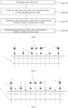
- FIG. 1 it is a flow chart of a method for preparing a silicon wafer according to the present application, and the specific preparation method includes the following steps:
- the non-metallic compound that is bonded with a silicon ion via a single bond is added in at least one of the cutting treatment, degluing treatment and cleaning treatment of the solar silicon ingot, Si dangling bonds on the surface of the silicon wafer are covalently bonded to the non-metallic compound, the dangling bonds on the surface of the prepared silicon wafer are basically eliminated, the interface activity is greatly reduced, and the bridging effect between silicon and oxygen can be effectively reduced.
- the residues of impurities such as metal ions and silicates on the surface of the silicon wafer can be blocked and the adsorption residues of metal ions and silicates on the surface of the silicon wafer and the formation of an oxide layer can be reduced, which is beneficial to the cleanliness and uniformity of texturing during preparation of a cell using the silicon wafer. Therefore, after the texturing, the silicon wafer has higher minority carrier lifetime, specific surface area and fill factor and the conversion efficiency of the solar cell prepared from the silicon wafer is improved.
- the preparation method of the present application is simple and needs additional steps, which can effectively reduce costs and improve cell efficiency.
- the surface of the silicon wafer is covered with non-metallic ions and forms a covalent compound, showing a certain degree of hydrophobicity, which can effectively reduce the adhesion of the metal ions on the surface of the silicon wafer.
- oxygen usually exists in the form of negative divalent ions, after oxygen ions are linked to Si, the other end of oxygen can be linked to a metal ion to form Si-O-M, where M can be a heavy metal ion, such as Fe, Cr, Ni, Cu, Mn, Zn, and the like and can also be a residual metal ion of silicates, such as Na, K, and the like.
- M can be a heavy metal ion, such as Fe, Cr, Ni, Cu, Mn, Zn, and the like and can also be a residual metal ion of silicates, such as Na, K, and the like.
- FIG. 2 shows a microscopic schematic diagram of the surface of the silicon wafer without passivation treatment, the dangling bonds 2 after cutting are easily linked to the oxygen ions 3 and metal ions 4 on the surface of the silicon wafer 1.
- the silicon dangling bonds can be preferentially linked to the non-metallic compound that is bonded with a silicon ion via a single bond, thereby reducing the bridging effect of the Si-O bond and further reducing the residues of metal ions and silicates on the surface of the silicon wafer.
- the non-metallic compound that is bonded with a silicon ion via a single bond includes at least one of a fluorine-containing compound, an iodine-containing compound, a hydrogen-containing compound, a bromine-containing compound, and a cyano-containing compound.
- the fluorine-containing compound includes an inorganic fluoride salt, including at least one of potassium fluoride, sodium fluoride, hydrogen fluoride, lithium fluoride, tetramethylammonium fluoride, tetraethylammonium fluoride, and ammonium fluoride.
- an inorganic fluoride salt including at least one of potassium fluoride, sodium fluoride, hydrogen fluoride, lithium fluoride, tetramethylammonium fluoride, tetraethylammonium fluoride, and ammonium fluoride.
- the iodine-containing compound includes at least one of potassium iodide, sodium iodide, tetramethylammonium iodide, tetraethylammonium iodide, ammonium iodide and p-iodophenol.
- the bromine-containing compound includes at least one of hydrogen bromide, potassium bromide, sodium bromide, lithium bromide, and ammonium bromide.
- the cyano-containing compound includes at least one of potassium cyanide, sodium cyanide, and ammonium cyanide.
- the non-metallic compound that is bonded with a silicon ion via a single bond includes at least one of a fluorine-containing compound and an iodine-containing compound.
- a single-bond compound that is more stable relative to the Si-O bond can be formed with silicon to ensure that the silicon wafer still has a protective effect during subsequent contact with water and air.
- the compound with a smaller ionic radius and a greater bond energy can be selected to highly ensure the formation of a stable compound on the surface of the silicon wafer.
- Most of the compounds formed by cyanide ions are toxic and their reactions are not easy to control, so they are used less frequently.
- the non-metallic compound single-bonded with the silicon ion includes a fluorine-containing compound.
- the non-metallic compound that is single-bonded with the silicon ion includes a fluorine-containing compound.
- the non-metallic compound that is bonded with a silicon ion via a single bond reacts with the surface of the silicon wafer and forms a layered structure, i.e., the passivation layer, on the surface of the silicon wafer.
- the existence of the passivation layer greatly reduces the residues of dangling bonds, metal ions and silicates on the surface of the silicon wafer and enhances the surface uniformity of the silicon wafer, which is beneficial to obtaining a more uniform and clean textured surface during the subsequent texturing.
- the mass ratio of the non-metallic compound that is bonded with a silicon ion via a single bond in at least one of the first treatment solution, the second treatment solution and the third treatment solution is less than or equal to 10%, specifically 0.05%, 0.1%, 0.5%, 0.8%, 1%, 1.5%, 2%, 3%, 4%, 5%, 6%, 7%, 8%, 9%, 10%, and the like.
- Controlling the mass ratio of the non-metallic compound that is bonded with a silicon ion via a single bond within the above range can ensure the normal cutting, degluing and cleaning of the solar silicon ingot and also can facilitate the combination of the silicon dangling bonds and the non-metallic compound that is bonded with a silicon ion via a single bond.
- the mass ratio of the non-metallic compound that is bonded with a silicon ion via a single bond in at least one of the first treatment solution, the second treatment solution and the third treatment solution is less than or equal to 2%.
- the conductivity of the first treatment solution is greater than 20 ⁇ s/cm.
- the conductivity of the first treatment solution may be 21 ⁇ s/cm, 23 ⁇ s/cm, 25 ⁇ s/cm, 26 ⁇ s/cm, 28 ⁇ s/cm , 30 ⁇ s/cm, 35 ⁇ s/cm, 38 ⁇ s/cm, and the like. Since the non-metallic compound that is bonded with a silicon ion via a single bond is a salt substance, its addition to the first treatment solution will increase the conductivity of the solution and further improve the conductivity of the solution.
- the conductivity of the first treatment solution is less than or equal to 20 ⁇ s/cm
- the dose of the non-metallic compound that is bonded with a silicon ion via a single bond is too small to react the dangling bonds on the surface of the silicon wafer.
- the solar silicon ingot is cut, there will be a certain amount of silicon powder in the environment. Due to the higher surface activity of the silicon powder, the non-metallic compound that is bonded with a silicon ion via a single bond will preferentially react with the silicon powder, but not with the surface of silicon wafer.
- the purpose of limiting the conductivity of the first treatment solution to be greater than 20 ⁇ s/cm is to ensure complete reaction with the dangling bonds on the surface of the silicon wafer, to ensure the formation of the passivation layer, and to further ensure the passivation effect.
- the non-metallic compound that is bonded with a silicon ion via a single bond can be added only in any one of the cutting process, the degluing process and the cleaning process, and can also be added in any combination of the above two processes.
- the non-metallic compound that is bonded with a silicon ion via a single bond can also be added in all of the above three treatment processes, which is not limited in the present application.
- step S100 a solar silicon ingot is provided.
- the solar silicon ingot of the present application may be prepared by using a wafer, or may be a commercially available silicon ingot purchased directly.
- step S200 the solar silicon ingot is cut with a first treatment solution to form a pretreated silicon wafer.
- the non-metallic compound that is bonded with a silicon ion via a single bond is added to the commercially available cutting solution for diamond wire cutting to form the first treatment solution.
- the dose of the non-metallic compound that is bonded with a silicon ion via a single bond varies according to stocks of cutting solutions sold by different producers.
- the conductivity of the first treatment solution is finally adjusted to be greater than 20 ⁇ s/cm, and then the solar silicon ingot is cut with the first treatment solution.
- a commercially available cutting solution includes the following components in percentage by mass as shown in Table 1: Table 1.
- Ammonium fluoride and potassium fluoride are added in the cutting solution of table 1, and the total mass of ammonium fluoride and potassium fluoride added to per kilogram of the cutting solution ranges from 5g to 12g.
- the mixed solution is then well mixed to obtain the first treatment solution.
- the conductivity of the first treatment solution is greater than 20 ⁇ s/cm and the fluoride ion content in the discharged wastewater does not exceed the national standard.
- dangling bonds 2 are exposed on the surface of the silicon wafer 1. A part of the dangling bonds 2 can be linked with the oxygen ions 3 in the cutting solution to form Si-O bonds, and the other end of the oxygen ions 3 is easily linked with the metal ion 4.
- F - and I - are added to the first treatment solution, there are at least F - , Fe 2+ , I - and other ions in the first treatment solution, and the corresponding standard electrode potentials are shown in Table 2 below. It can be seen that the F - ion formed by the most oxidizing fluorine element has better stability and a smaller ionic radius, and can quickly diffuse and bond to the silicon dangling bonds 2 with a certain positive electricity to form passivation.
- the electron cloud is easily deformed and can attract other metal ions 4 in the cutting solution, so that the resistance of the metal ions 4 to the surface of the silicon wafer 1 is increased, thereby avoiding the formation of Si-O bridging bonds on the surface of the silicon wafer 1, and further reducing the residues of metal ions 4, silicates, and the like on the surface of the silicon wafer 1 and improving the passivation effect of the silicon wafer.
- Table 2 The iodide ion has a large ionic radius, a large diffusion resistance, and a relatively weak attraction to the outermost electrons, the electron cloud is easily deformed and can attract other metal ions 4 in the cutting solution, so that the resistance of the metal ions 4 to the surface of the silicon wafer 1 is increased, thereby avoiding the formation of Si-O bridging bonds on the surface of the silicon wafer 1, and further reducing the residues of metal ions 4, silicates, and the like on the surface of the silicon wafer 1 and improving the passivation effect of the silicon wafer.
- step S300 the pretreated silicon wafer is deglued with a second treatment solution to obtain a deglued silicon wafer.
- the silicon ingot and an silicon ingot support need to be fixed with glue to ensure that the silicon ingot does not move during the cutting process. Therefore, the silicon wafer needs to be deglued and cleaned after wire cutting to obtain a highly clean silicon wafer.
- the degluing treatment refers to placing the pretreated silicon wafers in a second treatment solution for degluing.
- the second treatment solution includes a degluing solution and a non-metallic compound that is bonded with a silicon ion via a single bond.
- the degluing solution is generally an acidic solution, which includes lactic acid and citric acid, and the like.
- the degluing treatment can be performed at a certain temperature. In this way, the time for softening the glue can be shortened, the damaged layer on the surface of the silicon wafer can also be polished roughly, and the silicon wafer can also be prevented from being oxidized at a high temperature.
- Potassium fluoride is added to the lactic acid degluing solution and the mixed solution is well stirred to obtain a second treatment solution.
- the mass ratio of potassium fluoride in the second treatment solution is less than or equal to 10% (and not 0), which can ensure that the fluoride ion content in the wastewater discharged from the degluing treatment does not exceed the national standard.
- the step of removing impurities from the pretreated silicon wafer is further included prior to the degluing treatment.
- physical methods such as spray cleaning, ultrasonic cleaning, overflow cleaning, and the like, are used to remove impurities such as metal powder, silicon powder, silicon carbide, and cutting suspension attached to the surface of the pretreated silicon wafer.
- step S400 the deglued silicon wafer is cleaned with a third treatment solution to obtain the silicon wafer.
- the deglued silicon wafer is cleaned with a cleaning solution to further improve the cleanliness of the silicon wafer.
- ammonium fluoride with a mass ratio of not more than 0.5% is added to a H 2 O/NH 4 OH/H 2 O 2 cleaning tank, and the mixed solution was then well stirred to obtain the third treatment solution, which can ensure that the fluoride ion content in the wastewater discharged from the cleaning process does not exceed the national standard.
- the silicon wafer 1 is cleaned usually in an alkaline heating environment.
- the strong alkali makes the fluorine-containing ammonium salt easy to decompose ammonia gas.
- the continuous heating environment can drive away part of the ammonia gas from the water body and the ammonia gas is discharged to the outdoors by an exhaust system of the equipment.
- the relatively excess fluoride ions in the solution will further react with the Si-OH or Si-O- bonds formed by the oxygen ions 3 on the surface of the silicon wafer 1 to form more stable Si-F bonds, so that the residues of the metal ions 4 and silicates are excluded from the surface, resulting in passivation protection.
- the non-metallic compound that is bonded with a silicon ion via a single bond is added at least in the cutting process. It can be understood that there are many Si dangling bonds in the silicon wafer formed after the solar silicon ingot cutting process.
- the solution added in this process includes the non-metallic compound that is bonded with a silicon ion via a single bond. In this way, a stable compound layer can be formed on the surface of the silicon wafer in advance, which is beneficial to avoid the subsequent degluing and cleaning processes.
- the present application combines the process characteristics of silicon wafer cutting treatment, degluing treatment and cleaning treatment.
- the dangling bonds are most active when the silicon wafer is cut, the result with F - ion is the most stable, and the electron cloud of I - ion trading polarization deformation is more likely to bind positively charged metal ions; therefore, the present invention achieves the stabilization of the dangling bonds on the surface of the silicon wafer and the obstruction of the diffusion of metal ions.
- the present application further provides a silicon wafer, including: a silicon substrate 100, at least part of a surface of the silicon substrate being provided with a passivation layer 200, the passivation layer 200 including SiX y , where X is at least one of F, Br, I, H and CN.
- the surface of the silicon substrate 100 is the SiX y passivation layer 200, and the presence of the SiX y passivation layer can form a barrier on the surface of the silicon wafer to prevent impurities such as metal ions from reacting on the surface of the silicon wafer during the use of the silicon wafer, thereby improving the short-circuit current and parallel resistance of the solar cell prepared from the silicon wafer and improving the conversion efficiency of solar energy.
- the silicon substrate 100 may be an N-type substrate or a P-type substrate.
- the thickness of the silicon substrate 100 ranges from 110 ⁇ m to 250 ⁇ m.
- the thickness of the silicon substrate 100 can be 110 ⁇ m, 120 ⁇ m, 140 ⁇ m, 150 ⁇ m, 160 ⁇ m, 170 ⁇ m, 180 ⁇ m, 180 ⁇ m, 190 ⁇ m, 200 ⁇ m, 210 ⁇ m, 220 ⁇ m, 230 ⁇ m, 240 ⁇ m, 250 ⁇ m, and the like.
- the thickness of the silicon substrate 100 is not limited in the embodiments of the present application.
- y satisfies the following relationship: 1 ⁇ y ⁇ 3. It can be understood that the valence of Si is +4. After the solar silicon ingot is cut, the silicon atom on the surface of the silicon wafer is linked to at least one silicon atom inside the silicon wafer. Therefore, the silicon atom on the surface of the silicon wafer will have 1 to 3 Si dangling bonds, and the valence of X is -1. As a result, when 1 ⁇ y ⁇ 3, it can satisfy that the reaction between X ions and the silicon wafer forms a stable passivation reactant.
- the thickness of the passivation layer 200 ranges from 0.1 nm to 8 nm, and specifically may be 0.1 nm, 0.5 nm, 1 nm, 2 nm, 3 nm, 4 nm, 5 nm, 6 nm, 7 nm, and 8 nm.
- the passivation layer may be a part of the silicon wafer, and the passivation layer may also be a layered structure existing on the surface of the silicon wafer.
- the passivation layer 200 may be arranged on one surface of the silicon substrate 100, or on multiple surfaces of the silicon substrate 100. Preferably, the passivation layer 200 is arranged on the upper surface and lower surface of the silicon substrate 100.
- the present application further provides a passivation treatment solution, including a non-metallic compound that is bonded with a silicon ion via a single bond, the passivation treatment solution being used in at least one of cutting treatment, degluing treatment and cleaning treatment of a silicon wafer.
- the passivation treatment solution of the present application can passivate the silicon wafer in at least one of the cutting process, the degluing process and the cleaning process of the silicon wafer.
- the residues of dangling bonds, metal ions and silicates on the surface of the silicon wafer are greatly reduced and the uniformity of the surface of the silicon wafer is enhanced, which is beneficial to obtaining a more uniform and clean textured surface during the subsequent texturing of the silicon wafer.
- the mass ratio of the non-metallic compound that is bonded with a silicon ion via a single bond in the passivation treatment solution is less than or equal to 10% (and not 0), specifically 0.05%, 0.1%, 0.5%, 1%, 2%, 3%, 4%, 5%, 6%, 7%, 9%, and 10%.
- the non-metallic compound that is bonded with a silicon ion via a single bond includes at least one of a fluorine-containing compound, an iodine-containing compound, a hydrogen-containing compound, a bromine-containing compound, and a cyano-containing compound.
- the fluorine-containing compound includes an inorganic fluoride salt, including at least one of potassium fluoride, sodium fluoride, hydrogen fluoride, lithium fluoride, tetramethylammonium fluoride, tetraethylammonium fluoride, and ammonium fluoride.
- an inorganic fluoride salt including at least one of potassium fluoride, sodium fluoride, hydrogen fluoride, lithium fluoride, tetramethylammonium fluoride, tetraethylammonium fluoride, and ammonium fluoride.
- the iodine-containing compound includes at least one of potassium iodide, sodium iodide, tetramethylammonium iodide, tetraethylammonium iodide, ammonium iodide and p-iodophenol.
- the bromine-containing compound includes at least one of hydrogen bromide, potassium bromide, sodium bromide, lithium bromide, and ammonium bromide.
- the cyano-containing compound includes at least one of potassium cyanide, sodium cyanide, and ammonium cyanide.
- the passivation treatment solution when used in at least one of the cutting treatment, the degluing treatment and the cleaning treatment, the passivation treatment solution should be prepared and used on site before use, it is not suggested to prepare the passivation treatment solution in advance and use it after long-term storage.
- the time interval between the preparation of the passivation treatment solution and the use of the passivation treatment solution should be controlled within 30 min.
- a long silicon ingot with a length of 600mm is cut into 4 equal short silicon ingots, which are 1# silicon ingot, 2# silicon ingot, 3# silicon ingot, and 4# silicon ingot.
- the commercially available silicon wafer cleaning solution is H 2 O/NH 4 OH/H 2 O 2
- the commercially available silicon wafer degluing solution is lactic acid
- the formula of the commercially available cutting solution is shown in Table 1.
- the 1# silicon ingot was cut with a commercially available silicon wafer cutting solution to form a pretreated silicon wafer.
- the pretreated silicon wafer was deglued with a commercially available silicon wafer degluing solution to obtain a deglued silicon wafer.
- the deglued silicon wafer was cleaned with a commercially available silicon wafer cleaning solution to obtain a silicon wafer.
- the 2# silicon ingot was cut with a commercially available silicon wafer cutting solution to form a pretreated silicon wafer.
- the pretreated silicon wafer was deglued with a commercially available silicon wafer degluing solution to obtain a deglued silicon wafer.
- the deglued silicon wafer was cleaned with the third treatment solution to obtain a silicon wafer, wherein the third treatment solution included a mixed solution of a commercially available silicon wafer cleaning solution and ammonium fluoride, wherein the mass ratio of the ammonium fluoride in the third treatment solution was 0.5%.
- the third treatment solution included a mixed solution of a commercially available silicon wafer cleaning solution and ammonium fluoride, wherein the mass ratio of the ammonium fluoride in the third treatment solution was 0.5%.
- the 3# silicon ingot was cut with a commercially available silicon wafer cutting solution to form a pretreated silicon wafer.
- the pretreated silicon wafer was deglued with the second treatment solution to obtain a deglued silicon wafer, wherein the second treatment solution included a mixed solution of a commercially available silicon wafer degluing solution and potassium fluoride, and the mass ratio of potassium fluoride in the second treatment solution was 1%.
- the deglued silicon wafer was cleaned with the third treatment solution to obtain a silicon wafer, wherein the third treatment solution included a mixed solution of a commercially available silicon wafer cleaning solution and ammonium fluoride, wherein the mass ratio of the ammonium fluoride in the third treatment solution was 0.5%.
- the third treatment solution included a mixed solution of a commercially available silicon wafer cleaning solution and ammonium fluoride, wherein the mass ratio of the ammonium fluoride in the third treatment solution was 0.5%.
- the 4# silicon ingot was cut with the first treatment solution to form a pretreated silicon wafer.
- the first treatment solution included 1kg of a commercially available silicon wafer cutting solution, 2.6g of potassium fluoride and 7.34g of potassium iodide.
- the conductivity of the first treatment solution was 20.3 ⁇ s/cm.
- the pretreated silicon wafer was deglued with the second treatment solution to obtain a deglued silicon wafer, wherein the second treatment solution included a mixed solution of a commercially available silicon wafer degluing solution and potassium fluoride, and the mass ratio of potassium fluoride in the second treatment solution was 1%.
- the deglued silicon wafer was cleaned with the third treatment solution to obtain a silicon wafer, wherein the third treatment solution included a commercially available silicon wafer cleaning solution and ammonium fluoride, wherein the mass ratio of the ammonium fluoride in the third treatment solution was 0.5%.
- the third treatment solution included a commercially available silicon wafer cleaning solution and ammonium fluoride, wherein the mass ratio of the ammonium fluoride in the third treatment solution was 0.5%.
Landscapes
- Chemical & Material Sciences (AREA)
- Organic Chemistry (AREA)
- Inorganic Chemistry (AREA)
- Chemical Kinetics & Catalysis (AREA)
- Oil, Petroleum & Natural Gas (AREA)
- Life Sciences & Earth Sciences (AREA)
- Engineering & Computer Science (AREA)
- Wood Science & Technology (AREA)
- General Chemical & Material Sciences (AREA)
- Weting (AREA)
Applications Claiming Priority (1)
| Application Number | Priority Date | Filing Date | Title |
|---|---|---|---|
| CN202210745353.9A CN115148850B (zh) | 2022-06-27 | 2022-06-27 | 一种硅片及其制备方法、钝化处理溶液 |
Publications (1)
| Publication Number | Publication Date |
|---|---|
| EP4300601A1 true EP4300601A1 (de) | 2024-01-03 |
Family
ID=82839049
Family Applications (1)
| Application Number | Title | Priority Date | Filing Date |
|---|---|---|---|
| EP22188748.2A Pending EP4300601A1 (de) | 2022-06-27 | 2022-08-04 | Siliziumwafer, herstellungsverfahren eines siliziumwafers und passivierungsbehandlungslösung |
Country Status (3)
| Country | Link |
|---|---|
| US (1) | US12581890B2 (de) |
| EP (1) | EP4300601A1 (de) |
| CN (1) | CN115148850B (de) |
Citations (2)
| Publication number | Priority date | Publication date | Assignee | Title |
|---|---|---|---|---|
| US20140256078A1 (en) * | 2011-10-12 | 2014-09-11 | The Regents Of The University Of California | Semiconductor processing by magnetic field guided etching |
| CN107039241A (zh) * | 2017-03-09 | 2017-08-11 | 昆明理工大学 | 一种超薄硅的化学切割方法 |
Family Cites Families (15)
| Publication number | Priority date | Publication date | Assignee | Title |
|---|---|---|---|---|
| JP3772456B2 (ja) * | 1997-04-23 | 2006-05-10 | 三菱電機株式会社 | 太陽電池及びその製造方法、半導体製造装置 |
| KR100678482B1 (ko) | 2006-01-17 | 2007-02-02 | 삼성전자주식회사 | 실리콘 표면의 세정용액 및 이를 사용하는 반도체 소자의제조방법들 |
| JP2008060355A (ja) * | 2006-08-31 | 2008-03-13 | Sumco Corp | 貼り合わせウェーハの製造方法および貼り合わせウェーハ |
| US10453986B2 (en) * | 2008-01-23 | 2019-10-22 | Solvay Fluor Gmbh | Process for the manufacture of solar cells |
| US8329046B2 (en) * | 2009-02-05 | 2012-12-11 | Asia Union Electronic Chemical Corporation | Methods for damage etch and texturing of silicon single crystal substrates |
| CN101717937B (zh) | 2009-12-24 | 2012-02-22 | 浙江向日葵光能科技股份有限公司 | 一种用于制备单晶硅绒面的酸腐蚀溶液及其使用方法 |
| CN101817006A (zh) * | 2010-03-22 | 2010-09-01 | 浙江矽盛电子有限公司 | 一种太阳能硅片的表面清洗方法 |
| US8791026B2 (en) * | 2010-10-01 | 2014-07-29 | Mmtech Co., Ltd. | Method and apparatus for treating silicon substrate |
| WO2013128653A1 (ja) * | 2012-03-02 | 2013-09-06 | 株式会社クリスタル光学 | シリコンインゴットの切断方法 |
| CN102698983A (zh) * | 2012-05-08 | 2012-10-03 | 常州天合光能有限公司 | 一种太阳能级硅片的清洗方法 |
| CN102800758A (zh) * | 2012-08-28 | 2012-11-28 | 夏洋 | 一种晶硅太阳能电池表面钝化层仿生制备方法 |
| CN105810761B (zh) * | 2016-04-29 | 2018-07-27 | 南京工业大学 | 一种金刚线切割多晶硅片的制绒方法 |
| CN107104037B (zh) * | 2017-05-25 | 2019-06-21 | 中国工程物理研究院激光聚变研究中心 | 一种超薄单晶硅片的制备方法 |
| CN107845702A (zh) * | 2017-12-04 | 2018-03-27 | 浙江晶科能源有限公司 | 一种晶硅硅片的钝化层处理方法及晶硅太阳能电池 |
| CN113206172A (zh) * | 2021-04-16 | 2021-08-03 | 安徽华晟新能源科技有限公司 | 切片硅异质结电池及制备方法、太阳能电池组件 |
-
2022
- 2022-06-27 CN CN202210745353.9A patent/CN115148850B/zh active Active
- 2022-08-04 EP EP22188748.2A patent/EP4300601A1/de active Pending
- 2022-08-09 US US17/884,455 patent/US12581890B2/en active Active
Patent Citations (2)
| Publication number | Priority date | Publication date | Assignee | Title |
|---|---|---|---|---|
| US20140256078A1 (en) * | 2011-10-12 | 2014-09-11 | The Regents Of The University Of California | Semiconductor processing by magnetic field guided etching |
| CN107039241A (zh) * | 2017-03-09 | 2017-08-11 | 昆明理工大学 | 一种超薄硅的化学切割方法 |
Also Published As
| Publication number | Publication date |
|---|---|
| US12581890B2 (en) | 2026-03-17 |
| CN115148850B (zh) | 2023-06-02 |
| CN115148850A (zh) | 2022-10-04 |
| US20230420243A1 (en) | 2023-12-28 |
Similar Documents
| Publication | Publication Date | Title |
|---|---|---|
| CN111739985B (zh) | 太阳能电池及其选择性发射极的制备方法 | |
| KR101513911B1 (ko) | 태양 전지용 웨이퍼의 제조방법, 태양 전지 셀의 제조방법, 및 태양 전지 모듈의 제조방법 | |
| US8585918B2 (en) | Method of etching a silicon-based material | |
| US9099579B2 (en) | Photoelectric conversion device and manufacturing method thereof | |
| CN111525037A (zh) | 钙钛矿/N型TOPCon/钙钛矿叠层太阳能电池的制备方法及其电池 | |
| EP1753032A1 (de) | Halbleitersubstrat für eine solarzelle, herstellungsverfahren dafür und solarzelle | |
| EP2978026A1 (de) | Fotovoltaikelement und herstellungsverfahren dafür | |
| US11158748B2 (en) | Solar cell, solar cell module, and solar cell manufacturing method | |
| EP4300601A1 (de) | Siliziumwafer, herstellungsverfahren eines siliziumwafers und passivierungsbehandlungslösung | |
| JP6688244B2 (ja) | 高効率太陽電池の製造方法及び太陽電池セルの製造システム | |
| KR101528864B1 (ko) | 태양전지용 웨이퍼 및 그 제조 방법 | |
| CN111509089A (zh) | 一种双面太阳能电池及其制作方法 | |
| KR101642045B1 (ko) | 태양전지용 웨이퍼, 태양전지용 웨이퍼의 제조 방법, 태양전지 셀의 제조 방법, 및 태양전지 모듈의 제조 방법 | |
| US8697480B1 (en) | Method for treating a semiconductor | |
| JP5724718B2 (ja) | 太陽電池用ウェーハの製造方法、太陽電池セルの製造方法、および太陽電池モジュールの製造方法 | |
| CN103311093B (zh) | Pn结构的掺杂方法 | |
| JP5703780B2 (ja) | 太陽電池用ウェーハの製造方法、太陽電池セルの製造方法、および太陽電池モジュールの製造方法 | |
| JP5717743B2 (ja) | 太陽電池およびその製造方法、並びに太陽電池の製造装置 | |
| CN121888759A (zh) | 太阳能电池及光伏组件 | |
| CN118591894A (zh) | 使用硅颗粒的用于光伏器件的方法和系统 | |
| WO2012025984A1 (ja) | 半導体装置の製造装置及び半導体装置の製造方法 | |
| JPH04348569A (ja) | 太陽電池の製造方法 | |
| TW201039459A (en) | Processing method of semiconductor substrate |
Legal Events
| Date | Code | Title | Description |
|---|---|---|---|
| PUAI | Public reference made under article 153(3) epc to a published international application that has entered the european phase |
Free format text: ORIGINAL CODE: 0009012 |
|
| STAA | Information on the status of an ep patent application or granted ep patent |
Free format text: STATUS: REQUEST FOR EXAMINATION WAS MADE |
|
| 17P | Request for examination filed |
Effective date: 20220804 |
|
| AK | Designated contracting states |
Kind code of ref document: A1 Designated state(s): AL AT BE BG CH CY CZ DE DK EE ES FI FR GB GR HR HU IE IS IT LI LT LU LV MC MK MT NL NO PL PT RO RS SE SI SK SM TR |